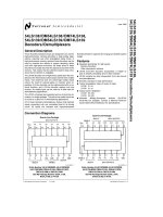
ĐIỆN tử VIỄN THÔNG 54LS138 khotailieu
Bạn đang xem bản rút gọn của tài liệu. Xem và tải ngay bản đầy đủ của tài liệu tại đây (165.36 KB, 8 trang )
54LS138 DM54LS138 DM74LS138
54LS139 DM54LS139 DM74LS139
Decoders Demultiplexers
General Description
These Schottky-clamped circuits are designed to be used in
high-performance memory-decoding or data-routing applications requiring very short propagation delay times In
high-performance memory systems these decoders can be
used to minimize the effects of system decoding When
used with high-speed memories the delay times of these
decoders are usually less than the typical access time of the
memory This means that the effective system delay introduced by the decoder is negligible
The LS138 decodes one-of-eight lines based upon the conditions at the three binary select inputs and the three enable
inputs Two active-low and one active-high enable inputs
reduce the need for external gates or inverters when expanding A 24-line decoder can be implemented with no external inverters and a 32-line decoder requires only one
inverter An enable input can be used as a data input for
demultiplexing applications
The LS139 comprises two separate two-line-to-four-line decoders in a single package The active-low enable input can
be used as a data line in demultiplexing applications
All of these decoders demultiplexers feature fully buffered
inputs presenting only one normalized load to its driving
circuit All inputs are clamped with high-performance
Schottky diodes to suppress line-ringing and simplify system
design
Features
Y
Y
Y
Y
Y
Y
Y
Designed specifically for high speed
Memory decoders
Data transmission systems
LS138 3-to-8-line decoders incorporates 3 enable inputs to simplify cascading and or data reception
LS139 contains two fully independent 2-to-4-line decoders demultiplexers
Schottky clamped for high performance
Typical propagation delay (3 levels of logic)
LS138 21 ns
LS139 21 ns
Typical power dissipation
LS138 32 mW
LS139 34 mW
Alternate
Military Aerospace
devices
(54LS138
54LS139) are available Contact a National Semiconductor Sales Office Distributor for specifications
Connection Diagrams
Dual-in-Line Package
Dual-in-Line Package
TL F 6391 – 1
Order Number 54LS138DMQB 54LS138FMQB
54LS138LMQB DM54LS138J DM54LS138W
DM74LS138M or DM74LS138N
See NS Package Number E20A J16A
M16A N16E or W16A
C1995 National Semiconductor Corporation
TL F 6391
TL F 6391 – 2
Order Number 54LS139DMQB 54LS139FMQB
54LS139LMQB DM54LS139J DM54LS139W
DM74LS139M or DM74LS139N
See NS Package Number E20A J16A
M16A N16E or W16A
RRD-B30M105 Printed in U S A
54LS138 DM54LS138 DM74LS138
54LS139 DM54LS139 DM74LS139 Decoders Demultiplexers
June 1989
Absolute Maximum Ratings (Note)
Note The ‘‘Absolute Maximum Ratings’’ are those values
beyond which the safety of the device cannot be guaranteed The device should not be operated at these limits The
parametric values defined in the ‘‘Electrical Characteristics’’
table are not guaranteed at the absolute maximum ratings
The ‘‘Recommended Operating Conditions’’ table will define
the conditions for actual device operation
If Military Aerospace specified devices are required
please contact the National Semiconductor Sales
Office Distributors for availability and specifications
Supply Voltage
7V
Input Voltage
7V
Operating Free Air Temperature Range
b 55 C to a 125 C
DM54LS and 54LS
DM74LS
0 C to a 70 C
Storage Temperature Range
b 65 C to a 150 C
Recommended Operating Conditions
Symbol
DM54LS138
Parameter
VCC
Supply Voltage
VIH
High Level Input Voltage
VIL
Low Level Input Voltage
IOH
High Level Output Current
IOL
Low Level Output Current
TA
Free Air Operating Temperature
DM74LS138
Units
Min
Nom
Max
Min
Nom
Max
45
5
55
4 75
5
5 25
2
2
V
07
08
V
b0 4
b0 4
mA
4
b 55
V
125
0
8
mA
70
C
Max
Units
b1 5
V
’LS138 Electrical Characteristics
over recommended operating free air temperature range (unless otherwise noted)
Symbol
Parameter
Conditions
Min
Typ
(Note 1)
VI
Input Clamp Voltage
VCC e Min II e b18 mA
VOH
High Level Output
Voltage
VCC e Min IOH e Max
VIL e Max VIH e Min
DM54
25
34
DM74
27
34
Low Level Output
Voltage
VCC e Min IOL e Max
VIL e Max VIH e Min
DM54
0 25
04
DM74
0 35
05
IOL e 4 mA VCC e Min
DM74
0 25
04
VOL
VCC e Max VI e 7V
V
II
Input Current
Input Voltage
IIH
High Level Input Current
VCC e Max VI e 2 7V
20
mA
IIL
Low Level Input Current
VCC e Max VI e 0 4V
b 0 36
mA
IOS
Short Circuit
Output Current
VCC e Max
(Note 2)
Supply Current
VCC e Max (Note 3)
ICC
Max
V
01
DM54
b 20
b 100
DM74
b 20
b 100
Note 1 All typicals are at VCC e 5V TA e 25 C
Note 2 Not more than one output should be shorted at a time and the duration should not exceed one second
Note 3 ICC is measured with all outputs enabled and open
2
63
10
mA
mA
mA
’LS138 Switching Characteristics
at VCC e 5V and TA e 25 C (See Section 1 for Test Waveforms and Output Load)
Symbol
Parameter
From (Input)
To (Output)
RL e 2 kX
Levels
of Delay
CL e 15 pF
Min
Max
CL e 50 pF
Min
Units
Max
tPLH
Propagation Delay Time
Low to High Level Output
Select to
Output
2
18
27
ns
tPHL
Propagation Delay Time
High to Low Level Output
Select to
Output
2
27
40
ns
tPLH
Propagation Delay Time
Low to High Level Output
Select to
Output
3
18
27
ns
tPHL
Propagation Delay Time
High to Low Level Output
Select to
Output
3
27
40
ns
tPLH
Propagation Delay Time
Low to High Level Output
Enable to
Output
2
18
27
ns
tPHL
Propagation Delay Time
High to Low Level Output
Enable to
Output
2
24
40
ns
tPLH
Propagation Delay Time
Low to High Level Output
Enable to
Output
3
18
27
ns
tPHL
Propagation Delay Time
High to Low Level Output
Enable to
Output
3
28
40
ns
Recommended Operating Conditions
Symbol
DM54LS139
Parameter
VCC
Supply Voltage
VIH
High Level Input Voltage
VIL
Low Level Input Voltage
IOH
High Level Output Current
IOL
Low Level Output Current
TA
Free Air Operating Temperature
DM74LS139
Units
Min
Nom
Max
Min
Nom
Max
45
5
55
4 75
5
5 25
V
07
08
V
b0 4
b0 4
mA
8
mA
70
C
2
2
4
b 55
125
3
0
V
’LS139 Electrical Characteristics
over recommended operating free air temperature range (unless otherwise noted)
Symbol
Parameter
Conditions
Min
Typ
(Note 1)
Max
Units
b1 5
V
VI
Input Clamp Voltage
VCC e Min II e b18 mA
VOH
High Level Output
Voltage
VCC e Min IOH e Max
VIL e Max VIH e Min
DM54
25
34
DM74
27
34
Low Level Output
Voltage
VCC e Min
VIL e Max
DM54
0 25
04
DM74
0 35
05
DM74
0 25
04
VOL
IOL e Max
VIH e Min
IOL e 4 mA VCC e Min
VCC e Max VI e 7V
V
II
Input Current
Input Voltage
IIH
High Level Input Current
VCC e Max VI e 2 7V
20
mA
IIL
Low Level Input Current
VCC e Max VI e 0 4V
b 0 36
mA
IOS
Short Circuit
Output Current
VCC e Max
(Note 2)
Supply Current
VCC e Max (Note 3)
ICC
Max
V
01
DM54
b 20
b 100
DM74
b 20
b 100
68
11
mA
mA
mA
Note 1 All typicals are at VCC e 5V TA e 25 C
Note 2 Not more than one output should be shorted at a time and the duration should not exceed one second
Note 3 ICC is measured with all outputs enabled and open
’LS139 Switching Characteristics
at VCC e 5V and TA e 25 C (See Section 1 for Test Waveforms and Output Load)
Symbol
From (Input)
To (Output)
Parameter
RL e 2 kX
CL e 15 pF
Min
CL e 50 pF
Max
Min
Units
Max
tPLH
Propagation Delay Time
Low to High Level Output
Select to
Output
18
27
ns
tPHL
Propagation Delay Time
High to Low Level Output
Select to
Output
27
40
ns
tPLH
Propagation Delay Time
Low to High Level Output
Enable to
Output
18
27
ns
tPHL
Propagation Delay Time
High to Low Level Output
Enable to
Output
24
40
ns
Function Tables
LS138
Inputs
Enable
LS139
Inputs
Outputs
Select
Enable
Outputs
Select
G1 G2
C B A YO Y1 Y2 Y3 Y4 Y5 Y6 Y7
G
B
A
Y0
Y1
Y2
Y3
X
L
H
H
H
H
H
H
H
H
X
X
L
L
L
L
H
H
H
H
H
L
L
L
L
X
L
L
H
H
X
L
H
L
H
H
L
H
H
H
H
H
L
H
H
H
H
H
L
H
H
H
H
H
L
H
X
L
L
L
L
L
L
L
L
X
X
L
L
H
H
L
L
H
H
X
X
L
H
L
H
L
H
L
H
H
H
L
H
H
H
H
H
H
H
H
H
H
L
H
H
H
H
H
H
H
H
H
H
L
H
H
H
H
H
H
H
H
H
H
L
H
H
H
H
H
H
H
H
H
H
L
H
H
H
H
H
H
H
H
H
H
L
H
H
H
H
H
H
H
H
H
H
L
H
H
H
H
H
H
H
H
H
H
L
H e High Level L e Low Level X e Don’t Care
G2 e G2A a G2B
H e High Level L e Low Level X e Don’t Care
4
Logic Diagrams
LS138
TL F 6391 – 3
LS139
TL F 6391 – 4
5
Physical Dimensions inches (millimeters)
Ceramic Leadless Chip Carrier Package (E)
Order Number 54LS138LMQB or 54LS139LMQB
NS Package Number E20A
16-Lead Ceramic Dual-In-Line Package (J)
Order Number 54LS138DMQB 54LS139DMQB DM54LS138J or DM54LS139J
NS Package Number J16A
6
Physical Dimensions inches (millimeters) (Continued)
16-Lead Small Outline Molded Package (M)
Order Number DM74LS138M or DM74LS139M
NS Packge Number M16A
16-Lead Molded Dual-In-Line Package (N)
Order Number DM74LS138N or DM74LS139N
NS Package Number N16E
7
54LS138 DM54LS138 DM74LS138
54LS139 DM54LS139 DM74LS139 Decoders Demultiplexers
Physical Dimensions inches (millimeters) (Continued)
16-Lead Ceramic Flat Package (W)
Order Number 54LS138FMQB 54LS139FMQB DM54LS138W or DM54LS139W
NS Package Number W16A
LIFE SUPPORT POLICY
NATIONAL’S PRODUCTS ARE NOT AUTHORIZED FOR USE AS CRITICAL COMPONENTS IN LIFE SUPPORT
DEVICES OR SYSTEMS WITHOUT THE EXPRESS WRITTEN APPROVAL OF THE PRESIDENT OF NATIONAL
SEMICONDUCTOR CORPORATION As used herein
1 Life support devices or systems are devices or
systems which (a) are intended for surgical implant
into the body or (b) support or sustain life and whose
failure to perform when properly used in accordance
with instructions for use provided in the labeling can
be reasonably expected to result in a significant injury
to the user
National Semiconductor
Corporation
1111 West Bardin Road
Arlington TX 76017
Tel 1(800) 272-9959
Fax 1(800) 737-7018
2 A critical component is any component of a life
support device or system whose failure to perform can
be reasonably expected to cause the failure of the life
support device or system or to affect its safety or
effectiveness
National Semiconductor
Europe
Fax (a49) 0-180-530 85 86
Email cnjwge tevm2 nsc com
Deutsch Tel (a49) 0-180-530 85 85
English Tel (a49) 0-180-532 78 32
Fran ais Tel (a49) 0-180-532 93 58
Italiano Tel (a49) 0-180-534 16 80
National Semiconductor
Hong Kong Ltd
13th Floor Straight Block
Ocean Centre 5 Canton Rd
Tsimshatsui Kowloon
Hong Kong
Tel (852) 2737-1600
Fax (852) 2736-9960
National Semiconductor
Japan Ltd
Tel 81-043-299-2309
Fax 81-043-299-2408
National does not assume any responsibility for use of any circuitry described no circuit patent licenses are implied and National reserves the right at any time without notice to change said circuitry and specifications