ĐIỆN tử VIỄN THÔNG 74hc595 khotailieu
Bạn đang xem bản rút gọn của tài liệu. Xem và tải ngay bản đầy đủ của tài liệu tại đây (178.59 KB, 8 trang )
MM54HC595 MM74HC595
8-Bit Shift Registers with Output Latches
General Description
Features
This high speed shift register utilizes advanced silicon-gate
CMOS technology This device possesses the high noise
immunity and low power consumption of standard CMOS
integrated circuits as well as the ability to drive 15 LS-TTL
loads
This device contains an 8-bit serial-in parallel-out shift register that feeds an 8-bit D-type storage register The storage
register has 8 TRI-STATE outputs Separate clocks are
provided for both the shift register and the storage register
The shift register has a direct-overriding clear serial input
and serial output (standard) pins for cascading Both the
shift register and storage register use positive-edge triggered clocks If both clocks are connected together the
shift register state will always be one clock pulse ahead of
the storage register
The 54HC 74HC logic family is speed function and pin-out
compatible with the standard 54LS 74LS logic family All
inputs are protected from damage due to static discharge by
internal diode clamps to VCC and ground
Y
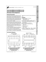
Connection Diagram
Truth Table
Dual-In-Line Package
Y
Y
Y
Y
Y
Y
Low quiescent current 80 mA maximum (74HC Series)
Low input current 1 mA maximum
8-bit serial-in parallel-out shift register
with storage
Wide operating voltage range 2V – 6V
Cascadable
Shift register has direct clear
Guaranteed shift frequency DC to 30 MHz
RCK
SCK
SCLR
G
Function
X
X
X
H
QA thru QH e TRI STATE
X
X
L
L
Shift Register cleared
Q He
X
u
H
L
Shift Register clocked
QN e Qn Q e SER
u
X
H
L
Contents of Shift
Register transferred
to output latches
TL F 5342 – 1
Top View
Order Number MM54HC595 or MM74HC595
TRI-STATE is a registered trademark of National Semiconductor Corp
C1995 National Semiconductor Corporation
TL F 5342
RRD-B30M105 Printed in U S A
MM54HC595 MM74HC595 8-Bit Shift Registers with Output Latches
January 1988
Absolute Maximum Ratings (Notes 1
Operating Conditions
2)
Min
If Military Aerospace specified devices are required
please contact the National Semiconductor Sales
Office Distributors for availability and specifications
Max
Supply Voltage VCC
DC Input or Output Voltage
VIN VOUT
b 0 5 to a 7 0V
Supply Voltage (VCC)
b 1 5 to VCC a 1 5V
DC Input Voltage (VIN)
b 0 5 to VCC a 0 5V
DC Output Voltage (VOUT)
g 20 mA
Clamp Diode Current (IIK IOK)
g 35 mA
DC Output Current per pin (IOUT)
g 70 mA
DC VCC or GND Current per pin (ICC)
b 65 C to a 150 C
Storage Temperature Range (TSTG)
Power Dissipation (PD)
(Note 3)
600 mW
S O Package only
500 mW
Lead Temp (TL) (Soldering 10 seconds)
260 C
Operating Temp Range (TA)
MM HC
MM HC
VCC
b
b
a
a
Input Rise or Fall Times
VCC e V
tr tf
VCC e V
VCC e V
Units
V
V
C
C
ns
ns
ns
DC Electrical Characteristics (Note 4)
Symbol
Parameter
Conditions
TA e 25 C
VCC
74HC
TA eb40 to 85 C
Typ
54HC
TA eb55 to 125 C
Units
Guaranteed Limits
VIH
Minimum High Level
Input Voltage
V
V
V
V
V
V
VIL
Maximum Low Level
Input Voltage
V
V
V
V
V
V
VOH
Minimum High Level
Output Voltage
VIN e VIH or VIL
lIOUTl s mA
V
V
V
V
V
V
QH
VIN e VIH or VIL
mA
lIOUTl s
lIOUTl s mA
V
V
V
V
VIN e VIH or VIL
mA
lIOUTl s
lIOUTl s mA
V
V
V
V
V
V
V
V
V
V
QA thru QH
VOL
Maximum Low Level
Output Voltage
VIN e VIH or VIL
lIOUTl s mA
QH
VIN e VIH or VIL
mA
lIOUTl s
lIOUTl s mA
V
V
V
V
VIN e VIH or VIL
mA
lIOUTl s
lIOUTl s mA
V
V
V
V
QA thru QH
IIN
Maximum Input
Current
VIN e VCC or GND
V
g
g
g
mA
IOZ
Maximum TRI STATE
Output Leakage
VOUT e VCC or GND
G e VIH
V
g
g
g
mA
ICC
Maximum Quiescent
Supply Current
VIN e VCC or GND
IOUT e mA
V
mA
Note 1 Absolute Maximum Ratings are those values beyond which damage to the device may occur
Note 2 Unless otherwise specified all voltages are referenced to ground
Note 3 Power Dissipation temperature derating
plastic ‘‘N’’ package b 12 mW C from 65 C to 85 C ceramic ‘‘J’’ package b 12 mW C from 100 C to 125 C
Note 4 For a power supply of 5V g 10% the worst case output voltages (VOH and VOL) occur for HC at 4 5V Thus the 4 5V values should be used when
designing with this supply Worst case VIH and VIL occur at VCC e 5 5V and 4 5V respectively (The VIH value at 5 5V is 3 85V ) The worst case leakage current (IIN
ICC and IOZ) occur for CMOS at the higher voltage and so the 6 0V values should be used
VIL limits are currently tested at 20% of VCC The above VIL specification (30% of VCC) will be implemented no later than Q1 CY’89
2
AC Electrical Characteristics VCC e 5V
Symbol
TA e 25 C tr e tf e 6 ns
Parameter
Conditions
Typ
Guaranteed
Limit
Units
fMAX
Maximum Operating
Frequency of SCK
MHz
tPHL tPLH
Maximum Propagation
Delay SCK to QH
CL e
pF
ns
tPHL tPLH
Maximum Propagation
Delay RCK to QA thru QH
CL e
pF
ns
tPZH tPZL
Maximum Output Enable
Time from G to QA thru QH
RL e kX
CL e pF
ns
tPHZ tPLZ
Maximum Output Disable
Time from G to QA thru QH
RL e kX
CL e pF
tS
Minimum Setup Time
from SER to SCK
ns
tS
Minimum Setup Time
from SCLR to SCK
ns
tS
Minimum Setup Time
from SCK to RCK
See Note
ns
tH
Minimum Hold Time
from SER to SCK
ns
tW
Minimum Pulse Width
of SCK or RCK
ns
ns
Note 5 This setup time ensures the register will see stable data from the shift-register outputs The clocks may be
connected together in which case the storage register state will be one clock pulse behind the shift register
AC Electrical Characteristics VCC e 2 0 – 6 0V
Symbol
Parameter
Conditions
VCC
CL e 50 pF tr e tf e 6 ns (unless otherwise specified)
TA e 25 C
Typ
74HC
TA eb40 to 85 C
54HC
TA eb55 to 125 C
Units
Guaranteed Limits
fMAX
Maximum Operating
Frequency
CL e
pF
V
V
V
MHz
MHz
MHz
tPHL tPLH
Maximum Propagation
Delay from SCK to Q H
CL e
CL e
pF
pF
V
V
ns
ns
CL e
CL e
pF
pF
V
V
ns
ns
CL e
CL e
pF
pF
V
V
ns
ns
CL e
CL e
pF
pF
V
V
ns
ns
CL e
CL e
pF
pF
V
V
ns
ns
CL e
CL e
pF
pF
V
V
ns
ns
tPHL tPLH
Maximum Propagation
Delay from RCK to QA thru QH
3
AC Electrical Characteristics
VCC e 2 0 – 6 0V CL e 50 pF tr e tf e 6 ns (unless otherwise specified) (Continued)
Symbol
Parameter
Conditions
TA e 25 C
VCC
Typ
tPHL tPLH
Maximum Propagation
Delay from SCLR to Q H
tPZH tPZL
Maximum Output Enable
from G to QA thru QH
74HC
TA eb40 to 85 C
54HC
TA eb55 to 125 C
Units
Guaranteed Limits
V
V
V
ns
ns
ns
RL e kX
CL e pF
pF
CL e
V
V
ns
ns
CL e
CL e
pF
pF
V
V
ns
ns
CL e
CL e
pF
pF
V
V
ns
ns
V
V
V
ns
ns
ns
tPHZ tPLZ
Maximum Output Disable
Time from G to QA thru QH
RL e kX
CL e pF
tS
Minimum Setup Time
from SER to SCK
V
V
V
ns
ns
ns
tR
Minimum Removal Time
from SCLR to SCK
V
V
V
ns
ns
ns
tS
Minimum Setup Time
from SCK to RCK
V
V
V
ns
ns
ns
tH
Minimum Hold Time
SER to SCK
V
V
V
ns
ns
ns
tW
Minimum Pulse Width
of SCK or SCLR
V
V
V
ns
ns
ns
tr tf
Maximum Input Rise and
Fall Time Clock
V
V
V
ns
ns
ns
tTHL tTLH
Maximum Output
Rise and Fall Time
QA QH
V
V
V
ns
ns
ns
tTHL tTLH
Maximum Output
Rise Fall Time
QH
V
V
V
ns
ns
ns
CPD
Power Dissipation
Capacitance Outputs
Enabled Note
CIN
Maximum Input
Capacitance
pF
COUT
Maximum Output
Capacitance
pF
G e VCC
G e GND
pF
pF
Note 6 CPD determines the no load dynamic power consumption PD e CPD VCC2 f a ICC VCC and the no load dynamic current consumption IS e CPD VCC f a ICC
4
Logic Diagram (positive logic)
TL F 5342 – 3
5
Timing Diagram
MM54HC595 MM74HC595
TL F 5342 – 2
6
Physical Dimensions inches (millimeters)
Order Number MM54HC595J or MM54HC595J
NS Package J16A
7
MM54HC595 MM74HC595 8-Bit Shift Registers with Output Latches
Physical Dimensions inches (millimeters) (Continued)
Order Number MM54HC595N
NS Package N16E
LIFE SUPPORT POLICY
NATIONAL’S PRODUCTS ARE NOT AUTHORIZED FOR USE AS CRITICAL COMPONENTS IN LIFE SUPPORT
DEVICES OR SYSTEMS WITHOUT THE EXPRESS WRITTEN APPROVAL OF THE PRESIDENT OF NATIONAL
SEMICONDUCTOR CORPORATION As used herein
1 Life support devices or systems are devices or
systems which (a) are intended for surgical implant
into the body or (b) support or sustain life and whose
failure to perform when properly used in accordance
with instructions for use provided in the labeling can
be reasonably expected to result in a significant injury
to the user
National Semiconductor
Corporation
1111 West Bardin Road
Arlington TX 76017
Tel 1(800) 272-9959
Fax 1(800) 737-7018
2 A critical component is any component of a life
support device or system whose failure to perform can
be reasonably expected to cause the failure of the life
support device or system or to affect its safety or
effectiveness
National Semiconductor
Europe
Fax (a49) 0-180-530 85 86
Email cnjwge tevm2 nsc com
Deutsch Tel (a49) 0-180-530 85 85
English Tel (a49) 0-180-532 78 32
Fran ais Tel (a49) 0-180-532 93 58
Italiano Tel (a49) 0-180-534 16 80
National Semiconductor
Hong Kong Ltd
13th Floor Straight Block
Ocean Centre 5 Canton Rd
Tsimshatsui Kowloon
Hong Kong
Tel (852) 2737-1600
Fax (852) 2736-9960
National Semiconductor
Japan Ltd
Tel 81-043-299-2309
Fax 81-043-299-2408
National does not assume any responsibility for use of any circuitry described no circuit patent licenses are implied and National reserves the right at any time without notice to change said circuitry and specifications