ĐIỆN tử VIỄN THÔNG MAX232N khotailieu
Bạn đang xem bản rút gọn của tài liệu. Xem và tải ngay bản đầy đủ của tài liệu tại đây (96.82 KB, 7 trang )
MAX232, MAX232I
DUAL EIA-232 DRIVER/RECEIVER
SLLS047H – FEBRUARY 1989 – REVISED FEBRUARY 2002
D
D
D
D
D
D
D
D
D
D
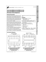
D, DW, N, OR NS PACKAGE
(TOP VIEW)
Operates With Single 5-V Power Supply
LinBiCMOS Process Technology
Two Drivers and Two Receivers
± 30-V Input Levels
Low Supply Current . . . 8 mA Typical
Meets or Exceeds TIA/EIA-232-F and ITU
Recommendation V.28
Designed to be Interchangeable With
Maxim MAX232
ESD Protection Exceeds JESD 22
– 2000-V Human-Body Model (A114-A)
Applications
TIA/EIA-232-F
Battery-Powered Systems
Terminals
Modems
Computers
Package Options Include Plastic
Small-Outline (D, DW, NS) Packages and
Standard Plastic (N) DIPs
C1+
VS+
C1–
C2+
C2–
VS–
T2OUT
R2IN
1
16
2
15
3
14
4
13
5
12
6
11
7
10
8
9
VCC
GND
T1OUT
R1IN
R1OUT
T1IN
T2IN
R2OUT
description
The MAX232 device is a dual driver/receiver that includes a capacitive voltage generator to supply EIA-232
voltage levels from a single 5-V supply. Each receiver converts EIA-232 inputs to 5-V TTL/CMOS levels. These
receivers have a typical threshold of 1.3 V and a typical hysteresis of 0.5 V, and can accept ± 30-V inputs. Each
driver converts TTL/CMOS input levels into EIA-232 levels. The driver, receiver, and voltage-generator
functions are available as cells in the Texas Instruments LinASIC library.
The MAX232 is characterized for operation from 0°C to 70°C. The MAX232I is characterized for operation from
– 40°C to 85°C.
AVAILABLE OPTIONS
PACKAGED DEVICES
SMALL
OUTLINE
(D, NS)
SMALL
OUTLINE
(DW)
PLASTIC DIP
(N)
0°C to 70°C
MAX232D
MAX232NS
MAX232DW
MAX232N
–40°C to 85°C
MAX232ID
MAX232IDW
MAX232IN
TA
The D and DW packages are available taped and reeled by adding an R to the part number
(i.e., MAX232DR). The NS package is only available taped and reeled.
Please be aware that an important notice concerning availability, standard warranty, and use in critical applications of
Texas Instruments semiconductor products and disclaimers thereto appears at the end of this data sheet.
LinASIC and LinBiCMOS are trademarks of Texas Instruments.
Copyright 2002, Texas Instruments Incorporated
PRODUCTION DATA information is current as of publication date.
Products conform to specifications per the terms of Texas Instruments
standard warranty. Production processing does not necessarily include
testing of all parameters.
POST OFFICE BOX 655303
• DALLAS, TEXAS 75265
1
MAX232, MAX232I
DUAL EIA-232 DRIVER/RECEIVER
SLLS047H – FEBRUARY 1989 – REVISED FEBRUARY 2002
absolute maximum ratings over operating free-air temperature range (unless otherwise noted)†
Input supply voltage range, VCC (see Note 1) . . . . . . . . . . . . . . . . . . . . . . . . . . . . . . . . . . . . . . . . . . – 0.3 V to 6 V
Positive output supply voltage range, VS+ . . . . . . . . . . . . . . . . . . . . . . . . . . . . . . . . . . . . . . . VCC – 0.3 V to 15 V
Negative output supply voltage range, VS – . . . . . . . . . . . . . . . . . . . . . . . . . . . . . . . . . . . . . . . . . . – 0.3 V to –15 V
Input voltage range, VI: Driver . . . . . . . . . . . . . . . . . . . . . . . . . . . . . . . . . . . . . . . . . . . . . . . – 0.3 V to VCC + 0.3 V
Receiver . . . . . . . . . . . . . . . . . . . . . . . . . . . . . . . . . . . . . . . . . . . . . . . . . . . . . . . . . . . ± 30 V
Output voltage range, VO: T1OUT, T2OUT . . . . . . . . . . . . . . . . . . . . . . . . . . . . . . . . VS – – 0.3 V to VS+ + 0.3 V
R1OUT, R2OUT . . . . . . . . . . . . . . . . . . . . . . . . . . . . . . . . . . . – 0.3 V to VCC + 0.3 V
Short-circuit duration: T1OUT, T2OUT . . . . . . . . . . . . . . . . . . . . . . . . . . . . . . . . . . . . . . . . . . . . . . . . . . . Unlimited
Package thermal impedance, θJA (see Note 2): D package . . . . . . . . . . . . . . . . . . . . . . . . . . . . . . . . . . . 73°C/W
DW package . . . . . . . . . . . . . . . . . . . . . . . . . . . . . . . . . 57°C/W
N package . . . . . . . . . . . . . . . . . . . . . . . . . . . . . . . . . . . 67°C/W
NS package . . . . . . . . . . . . . . . . . . . . . . . . . . . . . . . . . 64°C/W
Lead temperature 1,6 mm (1/16 inch) from case for 10 seconds . . . . . . . . . . . . . . . . . . . . . . . . . . . . . . . 260°C
Storage temperature range, Tstg . . . . . . . . . . . . . . . . . . . . . . . . . . . . . . . . . . . . . . . . . . . . . . . . . . – 65°C to 150°C
† Stresses beyond those listed under “absolute maximum ratings” may cause permanent damage to the device. These are stress ratings only, and
functional operation of the device at these or any other conditions beyond those indicated under “recommended operating conditions” is not
implied. Exposure to absolute-maximum-rated conditions for extended periods may affect device reliability.
NOTE 1: All voltage values are with respect to network ground terminal.
2. The package thermal impedance is calculated in accordance with JESD 51-7.
recommended operating conditions
VCC
VIH
Supply voltage
VIL
R1IN, R2IN
Low-level input voltage (T1IN, T2IN)
TA
2
High-level input voltage (T1IN,T2IN)
MIN
NOM
MAX
4.5
5
5.5
2
Receiver input voltage
Operating free
free-air
air temperature
POST OFFICE BOX 655303
• DALLAS, TEXAS 75265
UNIT
V
V
0.8
V
±30
V
MAX232
0
70
MAX232I
–40
85
°C
MAX232, MAX232I
DUAL EIA-232 DRIVER/RECEIVER
SLLS047H – FEBRUARY 1989 – REVISED FEBRUARY 2002
electrical characteristics over recommended ranges of supply voltage and operating free-air
temperature range (unless otherwise noted)
PARAMETER
TEST CONDITIONS
MIN
TYP†
7
T1OUT, T2OUT
RL = 3 kΩ to GND
5
R1OUT, R2OUT
3.5
T1OUT, T2OUT
IOH = – 1 mA
RL = 3 kΩ to GND
R1OUT, R2OUT
IOL = 3.2 mA
VOH
High level output voltage
High-level
VOL
Low level output voltage‡
Low-level
VIT+
Receiver positive-going input
threshold voltage
R1IN, R2IN
VCC = 5 V,
TA = 25°C
VIT–
Receiver negative-going input
threshold voltage
R1IN, R2IN
VCC = 5 V,
TA = 25°C
Vhys
Input hysteresis voltage
R1IN, R2IN
ri
Receiver input resistance
R1IN, R2IN
VCC = 5 V
VCC = 5,
ro
Output resistance
T1OUT, T2OUT
IOS§
Short-circuit output current
T1OUT, T2OUT
IIS
Short-circuit input current
T1IN, T2IN
ICC
Supply current
VS+ = VS – = 0,
VCC = 5.5 V,
VI = 0
VCC = 5.5 V,
TA = 25°C
–7
MAX
V
–5
0.4
TA = 25°C
VO = ± 2 V
1.7
UNIT
2.4
V
V
0.8
1.2
V
0.2
0.5
1
V
3
5
7
kΩ
Ω
300
±10
VO = 0
All outputs open,
8
mA
200
µA
10
mA
† All typical values are at VCC = 5 V, TA = 25°C.
‡ The algebraic convention, in which the least positive (most negative) value is designated minimum, is used in this data sheet for logic voltage
levels only.
§ Not more than one output should be shorted at a time.
switching characteristics, VCC = 5 V, TA = 25°C
PARAMETER
TEST CONDITIONS
MIN
TYP
MAX
UNIT
tPLH(R)
tPHL(R)
Receiver propagation delay time, low- to high-level output
See Figure 1
500
ns
Receiver propagation delay time, high- to low-level output
See Figure 1
500
ns
SR
Driver slew rate
RL = 3 kΩ to 7 kΩ,
See Figure 2
SR(tr)
Driver transition region slew rate
See Figure 3
POST OFFICE BOX 655303
• DALLAS, TEXAS 75265
30
3
V/µs
V/µs
3
MAX232, MAX232I
DUAL EIA-232 DRIVER/RECEIVER
SLLS047H – FEBRUARY 1989 – REVISED FEBRUARY 2002
PARAMETER MEASUREMENT INFORMATION
VCC
Pulse
Generator
(see Note A)
RL = 1.3 kΩ
R1OUT
or
R2OUT
R1IN
or
R2IN
See Note C
CL = 50 pF
(see Note B)
TEST CIRCUIT
≤ 10 ns
≤ 10 ns
Input
10%
90%
50%
90%
50%
3V
10%
0V
500 ns
tPLH
tPHL
VOH
Output
1.5 V
1.5 V
VOL
WAVEFORMS
NOTES: A. The pulse generator has the following characteristics: ZO = 50 Ω, duty cycle ≤ 50%.
B. CL includes probe and jig capacitance.
C. All diodes are 1N3064 or equivalent.
Figure 1. Receiver Test Circuit and Waveforms for tPHL and tPLH Measurements
4
POST OFFICE BOX 655303
• DALLAS, TEXAS 75265
MAX232, MAX232I
DUAL EIA-232 DRIVER/RECEIVER
SLLS047H – FEBRUARY 1989 – REVISED FEBRUARY 2002
PARAMETER MEASUREMENT INFORMATION
T1IN or T2IN
Pulse
Generator
(see Note A)
T1OUT or T2OUT
EIA-232 Output
CL = 10 pF
(see Note B)
RL
TEST CIRCUIT
≤ 10 ns
≤ 10 ns
90%
50%
Input
10%
3V
90%
50%
10%
0V
5 µs
tPLH
tPHL
90%
Output
90%
10%
10%
VOL
tTLH
tTHL
SR
+
VOH
0.8 (V
t
OH
–V
)
OL
0.8 (V
or
–V
)
OL OH
t
TLH
THL
WAVEFORMS
NOTES: A. The pulse generator has the following characteristics: ZO = 50 Ω, duty cycle ≤ 50%.
B. CL includes probe and jig capacitance.
Figure 2. Driver Test Circuit and Waveforms for tPHL and tPLH Measurements (5-µs input)
Pulse
Generator
(see Note A)
EIA-232 Output
3 kΩ
CL = 2.5 nF
TEST CIRCUIT
≤ 10 ns
≤ 10 ns
Input
90%
1.5 V
10%
90%
1.5 V
10%
20 µs
tTLH
tTHL
Output
3V
3V
–3 V
–3 V
SR
+t
THL
6 V
or t
VOH
VOL
TLH
WAVEFORMS
NOTE A:
The pulse generator has the following characteristics: ZO = 50 Ω, duty cycle ≤ 50%.
Figure 3. Test Circuit and Waveforms for tTHL and tTLH Measurements (20-µs input)
POST OFFICE BOX 655303
• DALLAS, TEXAS 75265
5
MAX232, MAX232I
DUAL EIA-232 DRIVER/RECEIVER
SLLS047H – FEBRUARY 1989 – REVISED FEBRUARY 2002
APPLICATION INFORMATION
5V
16
1 µF
C1+
3
From CMOS or TTL
To CMOS or TTL
2
VS –
C2+
5
6
+
C2–
11
14
10
7
12
13
8
9
0V
15
GND
Figure 4. Typical Operating Circuit
6
8.5 V
VS +
C1–
4
1 µF
1 µF
VCC
1
POST OFFICE BOX 655303
• DALLAS, TEXAS 75265
– 8.5 V
1 µF
EIA-232 Output
EIA-232 Output
EIA-232 Input
EIA-232 Input
IMPORTANT NOTICE
Texas Instruments Incorporated and its subsidiaries (TI) reserve the right to make corrections, modifications,
enhancements, improvements, and other changes to its products and services at any time and to discontinue
any product or service without notice. Customers should obtain the latest relevant information before placing
orders and should verify that such information is current and complete. All products are sold subject to TI’s terms
and conditions of sale supplied at the time of order acknowledgment.
TI warrants performance of its hardware products to the specifications applicable at the time of sale in
accordance with TI’s standard warranty. Testing and other quality control techniques are used to the extent TI
deems necessary to support this warranty. Except where mandated by government requirements, testing of all
parameters of each product is not necessarily performed.
TI assumes no liability for applications assistance or customer product design. Customers are responsible for
their products and applications using TI components. To minimize the risks associated with customer products
and applications, customers should provide adequate design and operating safeguards.
TI does not warrant or represent that any license, either express or implied, is granted under any TI patent right,
copyright, mask work right, or other TI intellectual property right relating to any combination, machine, or process
in which TI products or services are used. Information published by TI regarding third–party products or services
does not constitute a license from TI to use such products or services or a warranty or endorsement thereof.
Use of such information may require a license from a third party under the patents or other intellectual property
of the third party, or a license from TI under the patents or other intellectual property of TI.
Reproduction of information in TI data books or data sheets is permissible only if reproduction is without
alteration and is accompanied by all associated warranties, conditions, limitations, and notices. Reproduction
of this information with alteration is an unfair and deceptive business practice. TI is not responsible or liable for
such altered documentation.
Resale of TI products or services with statements different from or beyond the parameters stated by TI for that
product or service voids all express and any implied warranties for the associated TI product or service and
is an unfair and deceptive business practice. TI is not responsible or liable for any such statements.
Mailing Address:
Texas Instruments
Post Office Box 655303
Dallas, Texas 75265
Copyright 2002, Texas Instruments Incorporated