Influence of indium and hydrogen co-doping on optical and electrical properties of zinc oxide thin films deposited by DC magnetron sputtering
Bạn đang xem bản rút gọn của tài liệu. Xem và tải ngay bản đầy đủ của tài liệu tại đây (752.82 KB, 5 trang )
Science & Technology Development Journal, 22(2):253- 257
Original Research
Influence of indium and hydrogen co-doping on optical and
electrical properties of zinc oxide thin films deposited by DC
magnetron sputtering
Truong Huu Nguyen1,* , Tinh Van Nguyen1 , Anh Tuan Thanh Pham1 , Dung Van Hoang1 , Hung Minh Vu1 ,
Hoi Cong Nguyen1 , Thang Bach Phan2 , Vinh Cao Tran1
ABSTRACT
1
Laboratory of Advanced Materials,
University of Science, Vietnam National
University, Ho Chi Minh City
(VNU-HCM)
Introduction: ZnO-based thin films, known as potential transparent-conducting oxides (TCO),
have still attracted much attention in applications for good-performance electrodes and inner layers in solar cells. Recently, the research tendency has focused on improving carrier mobility rather
than carrier concentration to enhance performance and response speed of TCO thin films. In this
work, Indium, and Hydrogen co-doped ZnO (HIZO) thin films were deposited by using DC magnetron sputtering technique in hydrogen-plasma atmosphere. Methods: Indium-doped ZnO ceramics were used as sputtering targets, in which, Indium content varied from 0.07 to 1.0 at.%. The
electrical, optical, structural and surface morphological properties of the as-deposited films were investigated by using Hall effect-based measurement, UV-Vis spectra, X-ray diffraction (XRD) and fieldemission scanning electron microscopy (FE-SEM), respectively. Results: As a result, the HIZO films
sputtered from the 0.1 at.% In-doped ZnO target and at H2 /(H2 +Ar) ratio of 3.5% exhibit high electron mobility (47 cm2 /Vs), the lowest resistivity (4.9×10⁻⁴ Ω.cm) and sheet resistance (4.7 Ω/sq.),
simultaneously, high average transmittance (>80%) in the visible – near IR spectrum regions. Conclusion: Based on these results, the HIZO films are considered as potential TCO thin films that can
be well-used as transparent electrodes in solar cells.
Key words: indium and hydrogen co-doped ZnO, magnetron sputtering, TCO thin films, transparent electrodes
2
Center for Innovative Materials and
Architectures (INOMAR), Vietnam
National University, Ho Chi Minh City
(VNU-HCM)
Correspondence
Truong Huu Nguyen, Laboratory of
Advanced Materials, University of
Science, Vietnam National University, Ho
Chi Minh City (VNU-HCM)
Email:
History
• Received: 2019-02-25
• Accepted: 2019-05-28
• Published: 2019-06-25
DOI :
/>
Copyright
© VNU-HCM Press. This is an openaccess article distributed under the
terms of the Creative Commons
Attribution 4.0 International license.
INTRODUCTION
Transparent conducting oxide (TCO) thin films play
an essential role in optoelectronic devices. Until
now, Sn-doped In2 O3 (ITO) has still been the best
TCO with preeminent electrical and optical properties, which used as transparent electrodes. Because
of the scarcity of indium, however, it is essential
to explore new alternative TCO materials alternative
for ITO, which has attracted much attraction of researchers around the world. Based on the potential
properties of ZnO material, the IIIA-group elements
(such as Al, Ga, In) doping into ZnO thin films can
improve the conductivity owing to the increase of carrier concentration 1–3 . On the other hand, the increased carrier concentration often reduces the optical transmittance significantly, especially in the nearIR and IR spectrum regions, due to the free-carrier
absorption effect 4,5 . To solve this problem, increasing carrier mobility is expected to be more effective
than carrier concentration.
Hydrogen (H) is known as a dopant which can improve carrier mobility of ZnO films. There have been
many studies on H-doped ZnO films 4–8 , in which, a
few of them focused on H and In co-doped ZnO 6 . In
the report, however, the limitation is that the carrier
concentration was very high, leading to low electron
mobility (<30 cm2 /Vs). Therefore, in this work, the
combination of In and H in ZnO films is expected to
obtain high conductivity owing to the moderate freeelectron amount (from In dopant), and good crystalline quality (high mobility due to H incorporation). We prepare successfully In and H co-doped
ZnO (HIZO) thin films with low sheet resistance (RS
< 5 Ω/sq.), high electron mobility (> 40 cm2 /Vs) and
high average transmittance (>80%) in the wavelength
range from 400 nm to 1100 nm.
MATERIALS & METHOD
The ceramic In-doped ZnO sputtering targets were
synthesized by sintering ZnO and In2 O3 powders
at high temperature, which originated from Merck
(Germany) and high purity (99.99%). The compositions of the targets were changed and listed in Table 1.
The targets were used to deposit thin films on the glass
substrate (Marienfeld, Germany) by using DC mag-
Cite this article : Huu Nguyen T, Van Nguyen T, Thanh Pham A T, Van Hoang D, Minh Vu H, Nguyen H
C, Bach Phan T, Cao Tran V. Influence of indium and hydrogen co-doping on optical and electrical
properties of zinc oxide thin films deposited by DC magnetron sputtering. Sci. Tech. Dev. J.; 22(2):253257.
253
Science & Technology Development Journal, 22(2):253-257
Table 1: The composition of ZnO sputtering targets
with various In content
Targets
A
B
Dopants 0.07 0.1
C
D
0.15 0.3
E
F
G
0.5
1.0
0.0
(at.% In)
netron sputtering. For preparing HIZO thin films,
a small amount of hydrogen gas (5N, SunAir, Singapore) was introduced into the sputtering atmosphere. The added amount of hydrogen was calculated through partial pressure ratio, H2 /(H2 +Ar).
The substrate temperature and sputtering power were
maintained at 100◦ C and 60 W, respectively, while
the target-substrate distance was fixed at 5 cm during the deposition process. At each In content in target, at least three thin films were deposited, so as to
ensure repetition and accuracy in properties of the
HIZO films.
The thickness of films was about 1000 nm, which
was determined by using a Stylus profilometer (Veeco
DEKTAK 6M, Korea). The carrier concentration,
mobility, resistivity, and sheet resistance of the films
were obtained from Hall measurement with Van der
Pauw method (Ecopia HMS 3000, Korea) and the
four-point probe. X-ray diffraction (BRUKER D8
Advance, US) was used to determine the crystalline
structure of the films. The optical spectra were
recorded by UV-Vis spectrophotometer (Jasco V-530,
Japan) in the wavelength range of 300 - 1100 nm.
RESULT AND DISCUSSION
Electrical properties of the HIZO thin films from Hall
measurement at room temperature are summarized in
Table 2.
Through the electrical properties in Table 2, it is seen
that the HIZO films sputtered from the B target at
H2 /(H2 +Ar) = 3.5% obtain high electron mobility of
47.0 cm2 /Vs and the lowest resistivity of 4.9×10⁻⁴
Ω.cm, which corresponds to the lowest sheet resistance of 4.7 Ω/sq. From these results, the combination of In and H in ZnO films initially proposes the
significant enhancement in electrical properties of the
HIZO films. To evaluate the simultaneous influence
of In and H dopants, the optimum HIZO films are
compared to the pure ZnO films and the IZO films
(without H introduction). The electrical and optical
parameters of the three films are listed in Table 3.
Table 3 shows that the carrier concentration of the
sample B0 is higher than that of the sample G, but
lower than that of the sample B. Slassi et al. 9 and
254
Khuili et al. 10 reported that when a Zn atom is substituted by a IIIA-group atom, the Al 3s, Ga 4s or 4p and
In 5s orbitals contribute to the occupied states near
the Fermi level, which acts as a donor state around
the Fermi level. It may be considered as the origin
of the increased carrier concentration and electrical
conductivity of IIIA group-doped ZnO films. Furthermore, hydrogen also acts as a source contributing
electrons for conduction, with shallow donor states
below ~0.03 – 0.1 eV from the bottom of the conduction band 11,12 . The exciting thing is that the electron mobility of sample B reaches the highest values
of 47.3 cm2 /Vs. This value is considered much higher
than that of the other study on HIZO films 6 . The
reason can be from the excellent harmony of In and
H dopants in the lattice structure of ZnO films. To
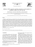
demonstrate this hypothesis, the crystalline structure
of the films are investigated through XRD spectra in
Figure 1.
From Figure 1, it is seen that all the films only have
a prominent ZnO (002) peak, indicating the typical hexagonal-wurtzite structure of ZnO material
(JCPDS 36-1451). No crystalline phases of In compounds are observed in the X-ray patterns, suggesting that In3+ probably replaces Zn2+ or locates in
interstitial sites in ZnO lattices or segregates in the
non-crystalline region at the grain boundaries 13 . The
HIZO films (sample B) have the (002) peak with the
highest intensity, which indicates that the addition of
the small amount of In and H can give rise to significant improvement in the crystalline quality of ZnO
films. Furthermore, the presence of hydrogen causing
the shift of (002) peak in sample B towards lower 2θ
angle as compared to sample G is observed. It suggests
the reduction of defects in the crystalline structure of
the sample B. Besides, the mean free paths (MFP) of
electron in the sample G, sample B0 and sample B
(2.5 nm, 3.2 nm and 7.1 nm, respectively) are much
smaller than their crystal size (26.9 nm, 30.4 and 29.6
nm, respectively). Thus, the grain boundary scattering cannot be the dominant mechanism affecting the
electron mobility. The increase in mobility value, as
shown in Table 3, therefore, can be due to the decrease
in ionized impurities scattering.
In literature, hydrogen can support In3+ substituting
into Zn2+ sites due to charge neutrality. The replacement acts an essential role in increasing In3+ donors,
which can be realized from the shift of (002) peak, as
mentioned in XRD patterns. As a result, the reduction
of scattering centers relating to interstitial impurities,
which leads to increase the mobility. Furthermore,
hydrogen can passivate some defects in the crystalline
Science & Technology Development Journal, 22(2):253-257
Table 2: Carrier concentration (n), electron mobility (µ ), resistivity (ρ ) and sheet resistance (RS ) of the HIZO films
n
(1020 cm−3 )
μ
(cm2 /Vs)
ρ
(10−4 Ω.cm)
RS
(Ω/sq.)
A
1.9
49.1
6.8
6.6
B
2.7
47.3
4.9
4.7
C
2.3
43.4
6.2
6.0
2.6
36.1
6.7
6.5
E
3.9
21.7
7.3
7.2
F
7.3
27.0
7.7
7.4
Films deposited
from targets
D
H2 /(H2 +Ar)
(%)
3.5
Table 3: Carrier concentration (n), electron mobility (µ ), resistivity (ρ ), sheet resistance (RS ), and average
transmittance in the visible (TVis ) and the near IR regions of the ZnO (sample G), IZO (sample B0) and HIZO
(sample B) films
Samples
H2 /(H2 +Ar)
(%)
n (x1020
cm−3 )
μ(cm2 /Vs)
ρ (10−4
Ω.cm)
RS (Ω/sq.)
TVis (%)
TNIR (%)
G
0
0.7
30.1
28.3
27.8
80.5
82.8
B0
0
1.2
32.1
15.9
14.6
78.1
79.1
B
3.5
2.7
47.3
4.9
4.7
81.5
82.0
Figure 1: X-ray diffraction patterns (left) and variations in peak position and crystal size of the ZnO, IZO and
HIZO films (right).
structure of ZnO, such as zinc vacancies (VZn ), dangling bonds 6–8 . This hydrogen passivation can occur through the adsorption and bonding formation
of O-H, Zn-H, or Zn-OH in crystalline grains, grain
boundaries, and film’s surface of ZnO films 6 .
During the deposition process, the effect of hydrogen
on the electrical properties, especially on the mobility
of the films can be observed. Another reason may be
the etching phenomenon in hydrogen plasma producing excited hydrogen atoms 14 . These excited H atoms
can make bonds with O atoms leading to the lack of
O atoms, which increases the number of O vacancies
and interstitial Zn. Therefore, the control of hydrogen
pressure is also the most important factor deciding the
electrical and structural properties of the HIZO thin
films.
Figure 2 illustrates the surface morphology of the
ZnO, IZO, and HIZO thin films. It is seen that the
grain density of sample B seems to be highest, while
the sample G has the lowest value. This is entirely
consistent with the improvement in the crystalline
structure and electrical properties of the films, as discussed in the XRD (Figure 1) and Hall measurement
(Tables 2 and 3) results. Additionally, in sample B,
the density of black spots tends to decrease. It is possible that In3+ ions can insert into the Zn vacancies.
255
Science & Technology Development Journal, 22(2):253-257
Figure 2: FE-SEM images of the G, B0 and B samples.
Simultaneously, H+ ions also fill up with O vacancies
and the black spots are enlarged at the grain boundaries. This suggests that H+ ions have been linked to
O2− ions at the surface, which removes small particles
from the surface of thin films 15 .
As mentioned in Table 3 and Figure 3, 1000-nmthick sample B has the lowest sheet resistance of 4.7
Ω/sq. and high average transmission over 80% in the
Vis –NIR region, which can be well used as transparent electrodes for solar cells.
TCO: Transparent Conducting Oxides
MFP: Mean Free Paths
ITO: Sn-doped In2 O3
XRD: X – Ray Diffraction
VZn : Zinc Vacancy
FE-SEM: Field Emission Scanning electron Microscopy
Vis–NIR: Visible and Near Infrared Range
CONCLUSION
The authors declare no competing interests.
A small amount of 0.1 at.% In-mixed ZnO sputtering
target and sputtering in hydrogen plasma are the optimum conditions for depositing good-performance
ZnO thin films. The carrier concentration increases
significantly from 0.7 to 2.7×1020 cm−3 due to In
donors. The electron mobility enhances by 67%,
thanks to the reasonable hydrogen ratio (3.5%). As a
result, the sheet resistance also decreases by 83% from
27.8 to 4.7 Ω/sq. Through this work, we propose that
the HIZO films can be used as transparent electrodes
in low-temperature applications (100◦ C).
AUTHORS’ CONTRIBUTIONS
ABBREVIATIONS
DC: Direct Current
256
COMPETING INTERESTS
Truong Huu Nguyen researched and wrote the paper. Vinh Cao Tran designed the study. Tinh Van
Nguyen, Anh Tuan Thanh Pham, Dung Van Hoang,
Hung Minh Vu, Hoi Cong Nguyen conducted the
experiments. Bach Thang Phan help to revise the
manuscript.
ACKNOWLEDGMENTS
The University of Science funded this research —
Vietnam National University, Ho Chi Minh City
(VNU-HCM) under Grant number T49-2017.
Science & Technology Development Journal, 22(2):253-257
Figure 3: Optical transmittance spectra of the G, B0 and B films.
The authors would like to thank the professors, reviewers, and technical committee of the Journal help
us to upgrade the quality of this paper.
REFERENCES
1. Peng LP. Characteristics of ZnO:In thin lms prepared by RF
magnetron sputtering. Physical E. 2009;41:1819–1823. Available from: 10.1016/j.physe.2009.07.006.
2. Jung K. Infuence of substrate temperature on the electrical
and optical properties of Ga-doped ZnO thin films fabricated
by continuous composition spread. Ceramics International.
2012;38S:S605–S608. Available from: 10.1016/j.ceramint.2011.
05.107.
3. Tubtimtae A, Lee MW. ZnO nanorods on undoped and indium
doped ZnO thin films as a TCO layer on nonconductive glass
for dye-sensitized solar cells. Superlattices and Microstructures. 2012;52:987–996. Available from: 10.1016/j.spmi.2012.
08.002.
4. Macco B, Knoops HCM, Verheijen MA, Beyer W, Creatore M,
Kessels WMM. Atomic layer deposition of high mobility hydrogen doped zinc oxide” Solar Energy Material and Solar cell”,
online 25.5.2017. 2017;Available from: 10.1016/j.solmat.2017.
05.040.
5. Dung HV, Khanh ND, Vinh TC. Deposition of high electron mobility transparent conducting aluminium doped zinc
oxide thin films by dc magnetron sputtering . Journal of
Science and Technology Vietnam. 2015;Available from: 10.
15625/2525-2518/54/1A/11821.
6. Singh A. On the temperature dependence of mobility in hydrogenated indium doped ZnO thin films. Acta Materialia.
2014;77:125–132. Available from: 10.1016/j.actamat.2014.05.
048.
7. Polyakov AY. Hydrogen plasma treatment effects on electrical
and optical properties of n-ZnO. Journal of Applied Physics.
2003;94:400. Available from: 10.1063/1.1579114.
8. Koch SG, et al.
Interplay between interstitial and substitutional hydrogen donors in ZnO.
Physical Review
B. 2014;89:235203. Available from: 10.1103/PhysRevB.89.
235203.
9. Slassi A, Naji S, Benyoussef A, Hamedoun M, Kenz AE. On
the transparent conducting oxide Al doped ZnO: First Principles and Boltzmann equations study. J Alloy Compd.
2014;605:118–123. Available from: 10.1063/1.1586977.
10. Khuili M, Fazouan N, Makarim HAE, Halani GE, Atmani EH.
Comparative first principles study of ZnO doped with group III
elements. J Alloy Compd. 2016;688:368–375. Available from:
10.1016/j.spmi.2012.03.012.
11. Willander M, Nur O, Sadaf JR, Qadir MI, Zaman S, Zainelabdin
A, et al. Luminescence from Zinc Oxide Nanostructures and
Polymers and their Hybrid Devices. Materials. 2010;3:2643–
2667. Available from: 10.1016/j.apsusc.2009.06.083.
12. Akazawa H. Hydrogen induced electric conduction in undoped ZnO and Ga-doped ZnO thin films: Creating native
donors via reduction, hydrogen donors, and reactivating extrinsic donors. J Vac Sci Technol A: Vacuum, Surfaces, and
Film. 2014;32:051511. Available from: 10.1016/j.jallcom.2014.
03.177.
13. Ko YD, Kim KC, Kim YS. Effects of substrate temperature
on the Ga-doped ZnO films as an anode material of organic
light emitting diodes. Superlattices and Microstructures.
2012;51(6):933–941. Available from: 10.1016/j.jallcom.2016.
06.294.
14. Wang L, et al. Temperature dependence of the free-exciton
transition energy in zinc oxide by photoluminescence excitation spectroscopy. Journal of Applied Physics. 2003;94:973–
978. Available from: 10.3390/ma3042643.
15. Park YR, et al. Effect of hydrogen doping in ZnO thin films by
pulsed DC magnetron sputtering. Applied Surface Sciences.
2009;255:9010–9014. Available from: 10.1116/1.4892777.
257