Microstrip bộ lọc cho các ứng dụng lò vi sóng RF (P7)
Bạn đang xem bản rút gọn của tài liệu. Xem và tải ngay bản đầy đủ của tài liệu tại đây (1.26 MB, 44 trang )
CHAPTER 7
Advanced Materials
and Technologies
High-temperature superconductors (HTS), ferroelectrics, micromachining or mi-
croelectromechanical systems (MEMS), hybrid or monolithic microwave integrated
circuits (MMIC), active filters, photonic bandgap (PBG) materials/structures, and
low-temperature cofired ceramics (LTCC) are among recent advanced materials
and technologies that have stimulated the rapid development of new microstrip and
other filters. This chapter summarizes some of these important materials and tech-
nologies, particularly regarding the applications to microstrip or stripline filters.
7.1 SUPERCONDUCTING FILTERS
High-temperature superconductivity is at the forefront of today’s filter technology
and is changing the way we design communication systems, electronic systems,
medical instrumentation, and military microwave systems [1–4]. Superconducting
filters play an important role in many applications, especially those for the next
generation of mobile communication systems [12–17]. Most superconducting fil-
ters are simply microstrip structures using HTS thin films [18–44]. For the design
of HTS microstrip filters, it is essential to understand some important properties of
superconductors and substrates for growing HTS films. These will be described in
the following section.
7.1.1 Superconducting Materials
Superconductors are materials that exhibit a zero intrinsic resistance to direct cur-
rent (dc) flow when cooled below a certain temperature. The temperature at which
the intrinsic resistance undergoes an abrupt change is referred to as the critical tem-
191
Microstrip Filters for RF/Microwave Applications. Jia-Sheng Hong, M. J. Lancaster
Copyright © 2001 John Wiley & Sons, Inc.
ISBNs: 0-471-38877-7 (Hardback); 0-471-22161-9 (Electronic)
perature or transition temperature, denoted by T
c
. For alternating current (ac) flow,
the resistance does not go to zero below T
c
, but increases with increasing frequency.
However, at typical RF/microwave frequencies (in the cellular band, for example),
the resistance of a superconductor is perhaps one thousandth of that in the best ordi-
nary conductor. It is certainly low enough to make significant improvement in per-
formances of RF/microwave microstrip filters.
Although superconductors were first discovered in 1911, for almost 75 years af-
ter the discovery, all known superconductors required a very low transition tempera-
ture, say 30 Kelvin (K) or lower; this limited the applications of these early super-
conductors. A revolution in the field of superconductivity occurred in 1986 with the
discovery of superconductors with transition temperatures greater than 77 K, the
boiling point of liquid nitrogen. These superconductors are therefore referred to as
the high-temperature superconductors (HTS). The discovery of the HTS made
world headlines since it made many practical applications of superconductivity pos-
sible. Since then, the development of microwave applications has proceeded vary
rapidly, particularly HTS microstrip filters.
The growth of HTS films and the fabrication of HTS microstrip filters are com-
patible with hybrid and monolithic microwave integrated circuits. Although there
are many hundreds of high-temperature superconductors with varying transition
temperatures, yttrium barium copper oxide (YBCO) and thallium barium calcium
copper oxide (TBCCO) are by far the two most popular and commercially available
HTS materials. These are listed in Table 7.1 along with their typical transition tem-
peratures [5].
7.1.2 Complex Conductivity of Superconductors
Superconductivity may be explained as a consequence of paired and unpaired elec-
trons travelling within the lattice of a solid. The paired electrons travel, under the in-
fluence of an electric field, without resistive loss. In addition, due to the thermal en-
ergy present in the solid, some of the electron pairs are split, so that some normal
electrons are always present at temperatures above absolute zero. It is therefore pos-
sible to model the superconductor in terms of a complex conductivity
1
– j
2
, and
such a model is called the two-fluid model [1–2].
A simple equivalent circuit is depicted in Figure 7.1, which describes complex
conductivity in superconductor. J denotes the total current density and J
s
and J
n
are
the current densities carried by the paired and normal electrons respectively. The to-
tal current in the circuit is split between the reactive inductance and the resistance,
which represents dissipation. As frequency decreases, the reactance becomes lower
192
ADVANCED MATERIALS AND TECHNOLOGIES
TABLE 7.1 Typical HTS materials
Materials T
c
(K)
YBa
2
Cu
3
O
7-x
(YBCO) Ϸ 92
Tl
2
Ba
2
Ca
1
Cu
2
O
x
(TBCCO) Ϸ 105
and more of the current flows through the inductance. When the current is constant,
namely at dc, this inductance completely shorts the resistance, allowing resistance-
free current flow.
As a consequence of the two-fluid mode, the complex conductivity may be given
by
=
1
– j
2
=
n
4
– j
΄
1 –
4
΅
(7.1)
where
n
is the normal state conductivity at T
c
and
0
is a constant parameter that
will be explained in the next section. Note that the calculation of (7.1) is not strictly
valid close to T
c
.
7.1.3 Penetration Depth of Superconductors
Normally the approximation
2
ӷ
1
can be made for good quality superconductors
provided that the temperature is not too close to the transition temperature, where
more normal electrons are present. Making this approximation, an important para-
meter called the penetration depth, based on the two-fluid model, is given by
= (7.2a)
Substituting
2
from (7.1) into (7.2a) yields
= (7.2b)
Thus
0
is actually the penetration depth as the temperature approaches zero Kelvin.
Depending on the quality of superconductors, a typical value of
0
is about 0.2 m
for HTS.
0
ᎏᎏ
Ί
1
–
ᎏ
T
T
c
ᎏ
4
1
ᎏ
͙
ෆ
ෆ
ෆ
2
ෆ
T
ᎏ
T
c
1
ᎏ
0
2
T
ᎏ
T
c
7.1 SUPERCONDUCTING FILTERS
193
J
J
s
J
n
σ
2
σ
1
Normal Current
Super Current
FIGURE 7.1 Simple circuit model depicting complex conductivity.
The penetration depth is actually defined as a characteristic depth at the surface
of the superconductor such that an incident plane wave propagating into the super-
conductor is attenuated by e
–1
of its initial value. It is analogous to the skin depth of
normal conductors, representing a depth to which electromagnetic fields penetrate
superconductors, and it defines the extent of a region near the surface of a super-
conductor in which current can be induced. The penetration depth
is independent
of frequency, but will depend on temperature, as can be seen from (7.2b). This de-
pendence is different from that of the skin depth of normal conductors. Recall that
the skin depth for normal conductors is
␦
=
Ί
(7.3)
where
n
is the conductivity of a normal conductor and is purely real. However, pro-
vided we are in the limit where
n
is independent of frequency, the skin depth is a
function of frequency.
Another distinguishing feature of superconductors is that a dc current or field
cannot penetrate fully into them. This is, of course, quite unlike normal conduc-
tors, in which there is full penetration of the dc current into the material. As a mat-
ter of fact, a dc current decays from the surface of superconductors into the mate-
rial in a very similar way to an ac current, namely, proportional to e
–z/
L
, where z
is the coordinate from the surface into the material and
L
is the London penetra-
tion depth. Therefore,
L
is a depth where the dc current decays by an amount e
–1
compared to the magnitude at the surface of superconductors. In the two-fluid
model, the value of the dc superconducting penetration depth
L
will be the same
as that of the ac penetration depth
given in (7.2) for
being independent of fre-
quency.
7.1.4 Surface Impedance of Superconductors
Another important parameter for superconducting materials is the surface imped-
ance. In general, solving Maxwell’s equation for a uniform plane wave in a metal of
conductivity
yields a surface impedance given by
Z
s
= =
Ί
(7.4)
where E
t
and H
t
are the tangential electric and magnetic fields at the surface. This
definition of the surface impedance is general and applicable for superconductors as
well. For superconductors, replacing
by
1
– j
2
gives
Z
s
=
Ί
(7.5a)
j
ᎏᎏ
(
1
– j
2
)
j
ᎏ
E
t
ᎏ
H
t
2
ᎏ
n
194
ADVANCED MATERIALS AND TECHNOLOGIES
whose real and imaginary parts can be separated, resulting in
Z
s
= R
s
+ jX
s
=
+ j
(7.5b)
with k = ͙
ෆ
1
2
ෆ
+
ෆ
ෆ
2
2
ෆ
. Using the approximations that k Ϸ
2
and ͙1
ෆ
±
ෆ
ෆ
1
/
ෆ
ෆ
2
ෆ
Ϸ 1 ±
1
/(2
2
) for
2
ӷ
1
, and replacing
2
with (
2
)
–1
, we arrive at
R
s
= and X
s
=
(7.6)
It is important to note that for the two-fluid model, provided
1
and
are independent
of frequency, the surface resistance R
s
will increase as
2
. This is of practical signif-
icance for justifying the applicability of superconductors to microwave devices as
compared with normal conductors, which will be discussed later. R
s
will depend on
temperature as well. Figure 7.2 illustrates typical temperature-dependent behaviors
of R
s
, where R
0
is a reference resistance. Also, the surface reactance in (7.6) may be
expressed as X
s
=
L, where the inductance L =
is called the internal or kinetic in-
ductance. The significance of this term lies in its temperature dependence, which will
mainly account for frequency shifting of superconducting filters against temperature.
For demonstration, Figure 7.3 shows a typical temperature dependence of an HTS
microstrip meander, open-loop resonator, obtained experimentally, where the reso-
nant frequency f
0
is normalized by the resonant frequency at 60 K. The temperature
2
2
1
3
ᎏᎏ
2
͙k
ෆ
–
ෆ
ෆ
1
ෆ
+ ͙k
ෆ
+
ෆ
ෆ
1
ෆ
ᎏᎏᎏ
k
͙k
ෆ
+
ෆ
ෆ
1
ෆ
– ͙k
ෆ
–
ෆ
ෆ
1
ෆ
ᎏᎏᎏ
k
͙
ෆ
ෆ
ᎏ
2
7.1 SUPERCONDUCTING FILTERS
195
FIGURE 7.2 Temperature dependence of surface resistance of superconductor.
stability of cooling systems for HTS filters can be better than 0.5 K; therefore, the fre-
quency shifting would not be an issue for most applications.
Films of superconducting material are the main constituents of filter applications,
and it is crucial for these applications that a good understanding of the properties of
these films be obtained. The surface impedance described above is actually for an in-
finitely thick film; it can be modified in order to take the finite thickness of the film
into account. If t is the thickness of the film, then its surface impedance is [1]
Z
f
= R
s
Ά
coth
+
·
+ jX
s
coth
(7.7)
where R
s
and X
s
are given by (7.6). Again
2
ӷ
1
is assumed in the derivation of
the expression. The effect of the finite thickness of thin film tends to increase both
the surface resistance and the surface reactance of thin film. Figure 7.4 plots the
surface resistance of the thin film as a function of t/
, indicating that in order to re-
duce the thin film surface resistance, the thin film thickness should be greater than
three to four times the penetration depth. This is similar to the requirement for nor-
mal conductor thin film microwave devices, where the conductor thickness should
at least three to four times thicker than the skin depth.
At this point, it is worthwhile comparing the surface resistance of HTS with that
of normal conductors. For a normal conductor, the surface resistance and surface re-
actance are equal and are given by
R
s
= X
s
=
Ί
(7.8)
ᎏ
2
n
t
ᎏ
1
ᎏ
sinh
2
ᎏ
t
ᎏ
t
ᎏ
t
ᎏ
196
ADVANCED MATERIALS AND TECHNOLOGIES
FIGURE 7.3 Temperature-dependent resonant frequency of a HTS microstrip resonator.
Both are proportional to the square root of frequency. Because the surface resistance
of a superconductor increases more rapidly (as frequency squared), there is a fre-
quency at which the surface resistance of normal conductors actually becomes lower
than that of superconductors. This has become known as the crossover frequency.
Figure 7.5 shows the comparison of the surface resistance of YBCO at 77 K with cop-
per, as a function of frequency. The typical values used to produce this plot are:
ț YBCO thin film surface resistance (10 GHz and 77 K) = 0.25 m⍀
ț Copper surface resistance (10 GHz and 77 K) = 8.7 m⍀
ț Copper surface resistance (10 GHz and 300 K) = 26.1 m⍀
In this case, the crossover frequency between copper and HTS films at 77 K is about
100 GHz.
It can also be seen from Figure 7.5 that at 2 GHz the surface resistance of HTS thin
film at 77 K is a thousand times smaller than that of copper at 300 K. Based on the
discussion on microstrip resonator quality factors in Chapter 4, we may reasonably
assume that a copper microstrip resonator has a conductor quality factor Q
c
= 250 at
2 GHz and 300 K. Since the conductor Q is inversely proportional to the surface re-
sistance, if the same microstrip resonator is made of HTS thin film, it follows imme-
diately that the Q
c
for the HTS microstrip resonator can be larger than 250 × 10
3
.
7.1.5 Nonlinearity of Superconductors
Microwave materials exhibit nonlinearity when they are subject to an extreme elec-
tromagnetic field, namely, their material properties such as conductivity, permittivi-
7.1 SUPERCONDUCTING FILTERS
197
FIGURE 7.4 Surface resistance of superconducting thin films as a function of normalized thickness.
ty, and permeability become dependent on the field. This is also true for HTS mate-
rials. It has been known that the surface resistance of an HTS film, which is related
to the conductivity as described above, will be degraded even when the RF peak
magnetic field in the film is only moderately high [6–8]. In the limit when the peak
magnetic field exceeds a critical value, the surface resistance rises sharply as the
HTS film starts losing its superconducting properties. This critical value of the RF
peak magnetic field is known as the critical field and may be denoted by H
rf,c
. The
H
rf,c
may be related to a dc current density by
J
c
= (7.9)
where
L
is the London penetration depth, which has the same value as that of
giv-
en by (7.2), and the J
c
is called the critical current density. J
c
is an important parame-
ter for characterization of HTS materials. It is temperature-dependent and has a typ-
H
rf,c
ᎏ
L
198
ADVANCED MATERIALS AND TECHNOLOGIES
FIGURE 7.5 Comparison of the surface resistance of YBCO at 77 K with copper as a function of fre-
quency.
ical value of about 10
6
A/cm
2
at 77 K for a good superconductor. Note that (7.9) is
valid only when the HTS film is several times thicker than the penetration depth.
Nonlinearity in the surface resistance not only increases losses of HTS filters,
but also causes intermodulation and harmonic generation problems. This, in gener-
al, limits the power handling of HTS filters. In many applications such as in a re-
ceiver, where HTS filters are operated at low powers, the nonlinear effects are either
negligible or acceptable. For high-power applications of HTS filters, the power-han-
dling capability of an HTS filter can, in general be increased in two ways. The first
method, from the HTS material viewpoint, is to increase the critical current density
J
c
by improving the material or to operate the filter at a lower temperature; J
c
will
increase as the temperature is decreased. The second method, from microwave de-
sign viewpoint, is to reduce the maximum current density in the filter by distribut-
ing the RF/microwave current more uniformly over a larger area. High-power HTS
filters handling up to more than 100 W have been demonstrated [37–44].
7.1.6 Substrates for Superconductors
Superconducting films have to be grown on some sort of substrate that must be in-
ert, compatible with the growth of good quality film, and also have appropriate mi-
crowave properties for the application purpose. In order to achieve good epitaxial
growth, the dimensions of the crystalline lattice at the surface of the substrate
should match the dimensions of the lattices of the superconductors. If this is not the
case, strain can be set up in the films, producing dislocations and defects. In some
cases, the substrates can react chemically, causing impurity levels to rise and the
quality of the film to fall. Cracks can be caused in the film if the thermal expan-
sions of the substrate and film are not appropriately matched. Some of the above
problems can be overcome by the application of a buffer layer between the films
and the substrates. In addition, the surface of substrates should be smooth and free
from defects and twinning if possible. These cause unwanted growth and mecha-
nisms that can lead to nonoptimal films. For microwave applications, it is of funda-
mental importance that the substrates have a low dielectric loss tangent (tan
␦
). If
the loss tangent is not low enough, then the advantage of using a superconductor
can be negated. It is also desirable in most applications that the dielectric constant,
or
r
, of a substrate not change much with temperature, improving the temperature
stability of the final applications. Whatever the dielectric constant, it must be repro-
ducible and not change appreciably from batch to batch. This is very important for
mass production.
With all the above requirements, it is not surprising that an ideal substrate for
HTS films has not been found yet. Nevertheless, a number of excellent substrates,
producing high-quality films with good microwave properties, are in common use.
Among these, the most widely used and commercially available substrates are lan-
thanum aluminate (LaAlO
3
or LAO), magesium oxide (MgO), and sapphire (Al
2
O
3
)
[9–11]. LaAlO
3
has a higher dielectric constant than MgO and sapphire but is gen-
erally twinned. Sapphire is a low loss and low cost substrate but its dielectric con-
stant is not isotropic and it requires a buffer layer to grow good HTS films. MgO is,
7.1 SUPERCONDUCTING FILTERS
199
in general, a very good substrate for applications but is mechanically brittle. Table
7.2 lists some typical parameters of these substrates. For sapphire substrate, the val-
ues of relative dielectric constants are given for both parallel and perpendicular to
the c-axis (crystal axis) because of anisotropy.
7.1.7 HTS Microstrip Filters
HTS microstrip filters are simply microstrip filters using HTS thin films instead of
conventional conductor films. In general, owing to very low conductor losses, the
use of HTS thin films can lead to significant improvement of microstrip filter per-
formance with regard to the passband insertion loss and selectivity. This is particu-
larly substantial for narrow-band filters, which play an important role in many ap-
plications. Some typical high-performance HTS filters are briefly described in the
following paragraphs.
A 19-pole HTS microstrip bandpass filter on a 75 mm diameter wafer has been de-
veloped [18]. The HTS filter has the same configuration as the pseudocombline fil-
ter discussed in Chapter 5 and uses an array of 19 straight half-wavelength microstrip
resonators. It was designed for the 900 MHz cellular communication band with 25
MHz bandwidth and is fabricated using double-side-coated YBCO films on a 0.5 mm
thick LaAlO
3
substrate. The YBCO films are thicker than 0.4 m. The filter pattern-
ing is accomplished by ion beam milling. The backside YBCO film is coated with a
silver/gold layer using an ion beam deposition technique at room temperature. This
normal metal layer provided an electrical contact between the ground plane and the
filter package. Measurement of the packaged filter at 77 K showed a dissipation loss
of 0.5 dB, corresponding to an average unloaded Q-factor of 10,000.
For narrow-band applications, a so-called hairpin-comb filter configuration [20]
may be used, in which the hairpin resonators all have the same orientation (see Fig-
ure 7.6) in order to achieve a weak coupling between adjacent resonators with a
small spacing. An 11-pole HTS microstrip filter of this type on a 50 mm diameter
wafer, where the 0.3 mm line width and the 1.3 mm inside spacing for each of the
hairpin resonators were determined based on the effectiveness of space usage [33],
has been produced. This HTS microstrip filter was developed for PCS (personal
communications services) applications. It was designed to have a 10 MHz passband
centered at 1.775 GHz and was fabricated using double-sided YBCO films on a 0.5
mm thick LaAlO
3
substrate. The YBCO films were about 0.3 m thick. The film
was patterned by conventional photolithography and the argon ion-milling method.
200
ADVANCED MATERIALS AND TECHNOLOGIES
TABLE 7.2 Substrates for HTS films
substrate
r
(typical) tan
␦
(typical)
LaAlO
3
24.2 @ 77K 7.6 × 10
–6
@ 77K and 10 GHz
MgO 9.6 @ 77K 5.5 × 10
–6
@ 77K and 10 GHz
Sapphire 11.6 || c-axis @ 77K 1.5 × 10
–8
@ 77K and 10 GHz
9.4 Ќ c-axis @ 77K
Gold (Au) electrodes were formed by lift-off process for electrical contact at the fil-
ter input/output. Also for the electrical contacts, 1 m thick Au film was deposited
on the top of the superconducting ground plane. After the gold deposition, the filter
was annealed at 480 °C in the flowing oxygen atmosphere. The packaged filter was
measured at 65 K. The measured minimum insertion loss was 0.6 dB. The measured
3 dB passband width was 11.5 MHz centered at 1.778 GHz.
To improve the selectivity of filters they can be designed to have elliptic or qua-
sielliptic function response. This is characterized by transmission nulls close to the
band edges. Figure 7.7(a) shows a HTS microstrip filter of this type [21]. It consists
of eight microstrip meander open-loop resonators. The configuration of resonators
not only allows both electric and magnetic coupling, but also allows cross coupling
between nonadjacent resonators to produce transmission zeros close to the passband
edges. The filter was developed for a digital mobile communication system
(DCS1800) as a preselect filter. It was designed to cover a passband from 1770
MHz to 1785 MHz. The HTS filter was produced using YBCO thin film HTS mate-
rial. This was deposited onto a MgO substrate 39 mm × 22.5 mm × 0.3 mm in size.
The measured transmission response of the filter at 55 K is illustrated in Figure
7.7(b), showing the characteristic of the quasielliptic function response with two di-
minishing transmission zeros near the passband edges, resulting in steeper skirts.
We will describe in more detail the development of this type of filter for mobile
base station applications in Chapter 12.
For typical applications at RF and low microwave frequencies it may be desirable
to make filters as small as possible for cost-effective use of thin film HTS wafers
and space-limited applications. To achieve miniaturization, filters can be construct-
ed using lumped or quasilumped elements. Numerous forms of lumped or quasi-
lumped element filters can be constructed, such as those described in [19], [27], and
[31]. We will discuss this subject further in Chapter 11.
7.1.8 High-Power HTS filters
The above-described HTS filters are primarily for low-power applications. Howev-
er, HTS filters can also be designed for high-power applications [37–44]. In gener-
al, there are three main factors that may limit the power handling of a RF/microwave
filter: (i) RF breakdown; (ii) heating in materials; and (iii) nonlinearity in materials.
For a HTS filter, the power handling limits are much the same. The RF breakdown
or arcing occurs at very high electric fields. Using a thicker dielectric substrate with
a lower dielectric constant and avoiding very small coupling gaps can reduce the
7.1 SUPERCONDUCTING FILTERS
201
Port 1
Port 2
FIGURE 7.6 Microstrip hairpin-comb bandpass filter configuration.
concentration of the electric field. Heating is associated with dissipation in materi-
als, including dielectrics and conductors. This may play a minor role in limiting the
power handling capability of a high-Q HTS filter using high-quality HTS film and a
low loss tangent substrate. Nonlinearity in materials particularly associated with the
nonlinear surface resistance of superconductors appears to be the major concern for
designing a high-power HTS filter.
Increasing input power of a HTS filter will arise the maximum current density at
the surface of superconductor. When the maximum current density exceeds the criti-
cal current density of the HTS material, the surface resistance rises sharply, causing
202
ADVANCED MATERIALS AND TECHNOLOGIES
FIGURE 7.7 (a) Eight-pole HTS microstrip quasielliptic function filter for DSC1800 on a MgO sub-
strate with a size of 39 mm × 22.5 mm × 0.3 mm. (b) Measured performance of the filter at 55 K.
the transition from its superconducting state into the nonsuperconducting state, and
eventually the collapse of the HTS filter performance. However, before the maximum
current density exceeds the critical current density, there is another effect due to the
nonlinear surface resistance, which may limit the power handling of a HTS filter. This
is the two-tone, third-order intermodulation (IMD). For nonlinear impedance Z =
Z(I), the voltage will be a nonlinear function of current, V(t) = I(t)Z(I) Ϸ a
1
I(t) +
a
2
I
2
(t) + a
3
I
3
(t) + ···. If we apply a two-tone fundamental signal I(t) = I
1
sin
1
t +
I
2
sin
2
t, it will produce intermodulation products at frequencies m
1
± n
2
where
m and n are integers. Among these products, the third-order IMD signals at 2
1
–
2
and 2
2
–
1
are of primary concern because they may fall in the filter passband,
causing interference with desired signals. To measure the two-tone, third-order IMD
in a filter, two-tone signals are usually adjusted to have the same power levels at the
filter input, and to have frequencies such that the third-order IMD signals are in the
passband of the filter. The power of the fundamental and the power of the third-order
IMD at the output of the filter are measured and plotted as a function of the applied
input power. In a log–log plot, the slope of the third-order IMD is about 3, compared
to 1 for the fundamental. Consequently, the situation arises wherein the output power
in the fundamental becomes equal to the output power in the third-order IMD. This
intercept point, measured in dBm, is known as the third-order intercept point (TOI or
IP3) and is used as a figure of merit for the nonlinearity present in the filter. A high
intercept indicates a high power handling capability of a filter. In practice, this inter-
cept may not be measured directly, but can be measured by plotting the levels of the
fundamental and two-tone intermodulation at lower power levels, and then using lin-
ear extrapolation to determine the intercept, as demonstrated in Figure 7.8.
From a microwave design viewpoint, an effective approach for reducing the non-
linear effects of a HTS filter is to reduce the current crowding in a superconductor.
7.1 SUPERCONDUCTING FILTERS
203
FIGURE 7. 8 Determining the third-order intercept point (IP3) by linear extrapolation of measured
data (plotted as symbols).
A simple way to achieve a more uniform current distribution is to increase mi-
crostrip line widths. An example of this is a five-pole HTS pseudocombline filter
with 1.2% fractional bandwidth centered on 2 GHz that uses half-wavelength res-
onators having a line characteristic impedance 10 ⍀ on 508 m thick LaAlO
3
sub-
strate and can handle 36 watts of power at 45 K [37].
Using patch or two-dimensional resonators for high-power filter designs is anoth-
er common approach [39–44]. A two-pole, high-power HTS filter has been devel-
oped based on a circular disk resonator [40]. This is a dual-mode filter that uses two
orthogonal degenerate TM
z
110
modes, and in order to couple the two modes, some sort
of perturbation on the perfect circular disk is required (refer to Chapter 11). In this
case, an elliptical deformation is used because the smooth shape is free from the field
concentration. The desired coupling can be obtained by suitably adjusting the ellip-
ticity of the disk shape so that the symmetric axes are oriented at 45° to the polariza-
tion directions of the modes. The filter is designed for a center frequency of 1.9 GHz
with a passband about 15 MHz, and in this case the diameter along to the major axis
is 19.6 mm with an ellipticity as low as 1%. The elliptic disk is capacitively coupled
to the input/output feed lines the filter. To avoid very narrow coupling gaps, which
may cause electric discharge for high-power operation, the width of each feed line is
expanded toward to its open end. The filter was fabricated using double-sided YBCO
thin films on 1 mm thick LaAlO
3
substrate. The two-tone, third-order intermodula-
tion measurement was performed with the two fundamental input signals of the fre-
quencies 1.905 and 1.910 GHz, and the input power up to 37.3 dBm. The generated
third-order IMD signals were at 1.900 and 1.915 GHz. The IP3 value, obtained by lin-
ear extrapolation, is 73 dBm (20 kW). High-power tests indicate that this high-power
HTS filter could have a power handling capability beyond 100 W [40].
As mentioned in Chapter 4 the TM
z
010
mode of a circular disk resonator is partic-
ularly of interest for design of high-power filters. This is because the disk resonator
operating at this mode does not have current at the edge and has a fairly uniform
current distribution along the azimuthal direction [41]. A ring resonator or a poly-
gon shape with sufficient number of sides can also operate at this mode. A four-
pole, high-power HTS filter comprised of an edge-current-free disk and ring res-
onators has been developed for extended C-band output multiplexers of
communication satellites [42]. The filter has a 40 MHz bandwidth at about 4.06
GHz with a power handling of 60 W and a third-order intercept point of higher than
83 dBm. Another two-pole filter of this type using two octagon-shaped resonators is
reported in [43]. The filter is made from double-sided Tl
2
Ba
2
CaCu
2
O
8
thin films on
0.508 mm thick LaAlO
3
with a size of 35mm × 17 mm, and is designed to have 1%
fractional bandwidth at 6.04 GHz. The measurements show that the performance of
this filter does not degrade up to 115 W of CW transmitting power at 77 K.
7.2 FERROELECTRIC TUNABLE FILTERS
Ferroelectrics have been studied since the early 1960s for application in microwave
devices [45] and their properties have been studied extensively in the intervening
204
ADVANCED MATERIALS AND TECHNOLOGIES
years. However, it is only relatively recently that applications are beginning to
emerge [46–57]. This recent renewed interest is due to a number of factors, such as
their compatibility with high-temperature superconductors in terms of their final
application and similar methods of production. The change in permittivity as a func-
tion of electric field is the key to a wide range of applications.
Frequency-agile filters are among many other device applications of ferro-
electrics. Such components have a wide range applications in many communica-
tions and radar systems. Frequency agility in microwave circuits can be realized us-
ing ferroelectric thin films incorporated into conventional microstrip circuits.
Electronically tunable filters can be produced with applications of interference sup-
pression, secure communications, dynamic channel allocation, signal jamming, and
satellite- and ground-based communications switching. Many new systems con-
cepts will appear as high-performance materials emerge; these systems will have
considerably improved performance over conventional systems.
Ferroelectric tunable filters are fast, small, lightweight, and, because they work
on electric fields, have low power consumption. The range of tuning is quite large
and devices are relatively simple in nature. The main problems currently being ad-
dressed are the relatively high loss tangents of the practical ferroelectric materials
and the large bias voltages required. This may be tackled by novel device structures.
Before we discuss ferroelectric tunable filters, some properties of ferroelectric ma-
terials will be described first.
7.2.1 Ferroelectric Materials
A ferroelectric material exhibits spontaneous polarization. Such a crystal can be
seen to contain positive and negative ions; in a certain temperature range the posi-
tive and negative ions are displaced. The displacement results in a net dipole mo-
ment. The orientation of the dipole moment in a ferroelectric can be shifted from
one state to another by the application of an electric field. The appearance of the
spontaneous polarization is highly temperature-dependent, and, in general, ferro-
electric crystals have phase transitions, where the crystal undergoes structural
changes [58]. This transition temperature is known as the Curie temperature (T
c
) at
which the material properties change abruptly.
Because of the nature of the crystal structure close to the Curie temperature,
thermodynamic properties show large anomalies. This is usually the case with the
dielectric constant, which increases to a large value close to the Curie temperature,
as demonstrated in Figure 7.9; it is also the point where there is the largest sensitiv-
ity of the dielectric constant to the application of an electric field. Some materials
that have shown a variable permittivity with electric field are SrTiO
3
, (Ba,Sr)TiO
3
,
(Pb,Sr)TiO
3
, (Pb,Ca)TiO
3
, Ba(Ti, Sn)O
3
, Ba(Ti, Zr)O
3
, and KTaO
3
dopants
[59–60].
However, strontium titanate (SrTiO
3
, STO) and barium strontium titanate (Ba
x
Sr
1–x
TiO
3
, BSTO), where x can vary from 0 to 1, are two of the most popular ferro-
electric materials current being studied for frequency-agile components and cir-
cuits. SrTiO
3
is of particular interest because of its crystalline compatibility with
7.2 FERROELECTRIC TUNABLE FILTERS
205
high-temperature superconductors (HTS) and its properties at low temperature.
Pure STO is supposed not to have Curie temperature above 0 K. Some thin films
and amorphous ceramic forms show a low-temperature peak in the dielectric con-
stant, implying that the Curie temperature is above 0 K, probably due to stresses or
impurities in the films. For BSTO, as the value of x varies from 0 to 1, the Curie
temperature varies from the value of STO to about 400 K, the Curie temperature of
BaTiO
3
(BTO). This allows tailoring of the Curie temperature; generally, a value of
x = 0.5 is used to optimize for room temperature, and a value of around 0.1 is used
when the material is to be used in conjunction with HTS films.
There are a number of different forms of these materials that are of interest for
applications. Single crystals have been studied for many years [62]. More recently,
thin films of the materials have been studied; these films are almost exclusively
made by laser ablation and are usually less than 1 m thick. The films are also pre-
dominately deposited on a LaAlO
3
substrate and are usually single layers with HTS
or a normal conductor placed on the top surface. However, tri-layer films have also
been produced, forming an HTS/Ferroelectric/HTS structure. Films on sapphire
have also been produced with a CeO
2
buffer layer to compensate for the lattice and
thermal expansion mismatch [67]. The sol–gel technique [70] for producing BST
has been developed more recently. This technique is able to produce material that is
of the order of 0.1 mm thick.
7.2.2 Dielectric Properties
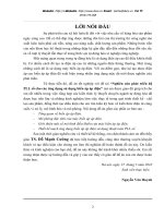
The dielectric constant of bulk single-crystal STO is known to be independent of
frequency up to 100–200 GHz [61–62]. The electric field and temperature depen-
dence of the dielectric constant of single crystal STO measured using a disk res-
206
ADVANCED MATERIALS AND TECHNOLOGIES
FIGURE 7.9 Curve of dielectric constant as a function of temperature.
onator at microwave frequencies [63] is shown in Figure 7.10. As can be seen, the
change in dielectric constant against an applied dc electric field is more sensitive at
a low temperature.
Table 7.3 shows a selection of measurements of the low-frequency properties of
some common ferroelectrics used for microwave applications. Measurements of the
relative dielectric constant (
r
) and loss tangent (tan
␦
) of STO and BSTO thin films
are not necessarily very consistent between film manufacturers; this is due to the
differing quality of the thin films. The loss tangent of STO single crystals is of the
order 2 × 10
–4
, however, in the thin film forms, this greatly increases, and almost all
7.2 FERROELECTRIC TUNABLE FILTERS
207
FIGURE 7. 10 (a) Temperature dependence of the STO dielectric constant at different dc electric
fields. (b) Electric field dependence of the STO dielectric constant. (Taken from [63], © 1996 by IEEE.)
Temperature, K
Dielectric constant
Electric field, kV/cm
Dielectric constant