Direct growth of graphitic carbongraphene on si (111) by using electron beam evaporation
Bạn đang xem bản rút gọn của tài liệu. Xem và tải ngay bản đầy đủ của tài liệu tại đây (14.5 MB, 155 trang )
university of namur
Research Center for the Physics of Matter and Radiation
Laboratoire de Physique des Mat´
eriaux Electroniques
DIRECT GROWTH OF GRAPHITIC
CARBON/GRAPHENE ON Si(111) BY USING
ELECTRON BEAM EVAPORATION
Presented by Trung T. PHAM
Dissertation
For the Degree of DOCTOR IN SCIENCES
Jury Members:
President: Professor Laurent HOUSSIAU (University of Namur)
Examiners: Doctor Jacques DUMONT (R & D Centre, AGC Glass Europe)
Professor Jean-Marc THEMLIN (University of Aix Marseille)
Professor Olivier DEPARIS (University of Namur)
Supervisor: Professor Robert SPORKEN (University of Namur)
October 15, 2015
Acknowledgments
First, I would like to sincerely thank my supervisor, Robert SPORKEN, for welcoming
and giving me the opportunity to do research in his laboratory (LPME). He encouraged
me and always created the best conditions for me during my PhD study, but at the same
time let me autonomous. In particular, I am very grateful to him for all his help about
our family reunion (my wife and my daughter). We are very happy to live together in
Belgium. This will be the most memorable time in our living abroad. Thanks to that, I
have had a good motivation to complete my PhD thesis.
Next, I also would like to thank
❼ Vietnam International Education Development (VIED) for financial support during
my four-year PhD study in Belgium. In particular, I am very appreciated Director
of VIED, Mr. Vang X. NGUYEN, for his valuable advices and enthusiastic
encouragements.
❼ The university of Technology and Education of HCMC for their agreement with me
to obtain the fellowship from Vietnam government for four-year study in Belgium.
For all the members of the laboratory (LPME), I would like to say the most thankful
words to
❼ Etienne GENNART for technical support in time and other help for our living. A
funny member who often makes a lot of rememberable jokes. Thanks so much!
❼ Fernande FRISING and Jean-Pierre VAN ROY for the valuable encouragements.
❼ Fr´ed´eric JOUCKEN, a friendly colleague, his numerous scientific advices and
fruitful discussions helped me a lot during these 4 years of research.
❼ Dodji AMOUZOU and Paul THIRY for helpful discussions.
Among the members of Namur University, many thanks go to
i
❼ Mac MUGUMAODERHA Cubaka for guiding me in technical and experimental
steps at the beginning of my study. His support helped me a lot to be familiar
with the initial experiments.
❼ Nicolas RECKINGER for helping in Raman measurement, guiding me for doing
graphene transfer and nice discussions.
❼ Francesca CECCHET for helping in AFM analyses and useful discussions.
❼ Benjamin BERA for helping in Magnetron sputtering of SiO2 on my samples and
discussions.
❼ Jacques GHIJSEN for helping UPS analyses in Hamburg, Alexandre FELTEN,
Laurent NITTLER, Pierre LOUETTE for XPS and Jean-Fran¸cois COLOMER for
SEM measurements.
❼ Jean-Paul LEONIS for assisting the paperworks whenever I met problems.
❼ Mrs. Cathy JENTGEN, Mrs. Florence COLLOT and Mr. Charles DEBOIS for
their arrangement of our accommodation at an apartment of the university during
my study.
My acknowledgements are also dedicated to Benoit HACKENS, Cristiane N. SANTOS,
Jessica CAMPOS-DELGADO, S´ebastien FANIEL for Raman and HR-SEM annalyses
with useful discussions and Jean-Pierre RASKIN, Pierre-Antoine HADDAD for training
on fabrication of graphene field-effect transistors at WINFAB in Universit´e Catholique
de Louvain (UCL) with interesting discussions/suggestions.
In addition, I would also like to thank all members of the jury for having kindly accepted
to evaluate my work and the University of Namur for funding conferences, workshops
and scientific stays.
Last but not least in my heart, all my thankfulness to my little family (my wife - Nuong
and my daughter - Nguyen), my father, my parents in law, brothers, sister and to all my
friends encouraged and always stayed beside me during my study abroad.
Thank you all!
Trung T. PHAM
Namur - Belgium
August 15, 2015
ii
Abstract
Graphene has recently emerged as a promising material due to its outstanding electrical,
optical, thermal, and mechanical properties. It opens new possibilities not only for
fundamental physics research but also for industrial applications. Nowadays, since silicon
is still the most important single-crystal substrate used for semiconductor devices and
integrated circuits, integration of graphene into the current Si technology is highly
desirable. A combination between graphene and silicon may overcome the traditional
limitations in scaling down of devices that silicon-based technology is facing. Graphene
on Si might be one of the most promising candidates as a material for graphene-based
technology beyond CMOS. Therefore, it is crucial to find a process to grow graphene
directly on Si.
In this thesis, we chose Si(111) as a substrate for graphene formation by electron beam
evaporation because its surface has an interesting multi-layer reconstruction driven by
the minimization of dangling bonds at the surface compared with other oriented Si. It
exhibits a six-fold symmetry and is the most stable surface among various orientations
of Si. Therefore, it is expected to be an appropriate substrate for graphitic carbon
growth. However, due to the huge lattice mismatch between graphene (aG = 2.46 Å)
and Si(111) (aSi1×1 = 3.84 Å), it is not easy to grow directly graphene on Si(111) and
a buffer is considered as a solution to reduce the lattice mismatch. In this context, we
have proposed a structural model using amorphous carbon (a-C) and/or SiC as a buffer
on Si(111) with different configurations such as C/a-C/Si(111), C/a-C/3C -SiC/Si(111),
C/3C -SiC/Si(111) or C/Si/3C -SiC/Si(111) (C stands for the graphitic layer). The
quality of the graphitic layer depends not only on the substrate temperature but also on
the growth time and on the thickness of the buffer layer. In addition, we also found that
silicon diffuses through the SiC buffer layer during the graphene growth and reduces
the quality of epitaxial graphene. Therefore, a calculation of the silicon diffusion profile
through the SiC buffer layer during carbon deposition is presented to explain how the
crystalline quality of graphene depends on the details (annealing temperature, growth
time, etc.) of the growth process.
iii
R´
esum´
e
Le graph`ene a r´ecemment ´emerg´e comme un mat´eriau prometteur en raison de ses
propri´et´es exceptionnelles tant ´electriques, optiques, thermiques que m´ecaniques. Il
ouvre de nouvelles possibilit´es, non seulement pour la recherche en physique fondamentale,
mais aussi pour les applications industrielles. Actuellement, puisque le silicium est encore
le substrat monocristallin le plus important utilis´e pour la fabrication des dispositifs
semi-conducteurs et des circuits int´egr´es, l’int´egration du graph`ene dans la technologie
silicium est hautement souhaitable. Une combinaison entre graph`ene et silicium peut
aider a` d´epasser les limites de miniaturization rencontr´ees par l’industrie. Le graph`ene sur
silicium est un candidat prometteur pour d´epasser la technologie CMOS. Par cons´equent,
trouver un processus pour faire croˆıtre le graph`ene directement sur silicium est un sujet
important.
Dans cette th`ese, nous avons choisi le Si(111) comme substrat pour la formation du
graph`ene en utilisant l’´evaporation par faisceau d’´electrons parce que sa surface pr´esente
une reconstruction int´eressante entraˆın´ee par la minimisation des liaisons pendantes
compar´ee aux autres surfaces du silicium. Elle pr´esente une sym´etrie hexagonale et est la
surface la plus stable parmi les orientations du silicium. Par cons´equent, il est consid´er´e
comme un substrat appropri´e pour la croissance du carbone graphitique. Cependant, a`
cause de la grande diff´erence des param`etres de maille entre le graph`ene (aG = 2.46 Å) et
le Si(111) (aSi1×1 = 3.84 Å), il n’est pas ais´e de faire croˆıtre directement le graph`ene sur
le Si(111) et une couche tampon peut ˆetre consid´er´ee comme une solution `a ce probl`eme.
Dans ce contexte, nous avons propos´e un mod`ele utilisant le carbone amorphe (a-C) ainsi
que le SiC comme couche tampon, en diff´erentes combinaisons, telles que C/a-C/Si(111),
C/a-C/3C -SiC/Si(111), C/3C -SiC/Si(111) ou C/Si/3C -SiC/Si(111) (C repr´esente la
couche graphitique). La qualit´e de la couche graphitique d´epend de la temp´erature du
substrat mais aussi du temps de croissance et de l’´epaisseur de la couche tampon. Nous
avons aussi trouv´e que le silicium du substrat diffuse au travers de la couche tampon de
SiC pendant la croissance du graph`ene ce qui r´eduit la qualit´e du graph`ene obtenu. Nous
pr´esentons en outre un calcul du profil de diffusion du silicium qui explique comment la
qualit´e du graph`ene d´epend des d´etails du processus de croissance.
Keywords: Graphitic carbon, graphene on Si, buffer layer, electron beam evaporation,
Si diffusion.
iv
List of abbreviations
Abbreviation
0D
1D
2D
3D
a-C
AES
AFM
BCC
CMP
CMOS
CVD
DAS
FCC
FWHM
g-C
G-FETs
GO
HAC
HOPG
HR-SEM
HV
IMFP
FFT
FT-IR
LEED
LED
LO
LPME
MBE
MFP
ML
MWCNTs
NEXAFS
PMMA
Full name
Zero dimension
One dimension
Two dimensions
Three dimensions
amorphous carbon
Auger electron spectroscopy
Atomic force microscope
Body-centered cubic
Chemomechanical polishing
Complementary metal-oxide-semiconductor
Chemical vapor deposition
Dimer-adatom-stacking
Face-centered cubic
Full width at half maximum
graphitic carbon
Graphene field-effect transistors
Graphene oxide
Hydrogenated amorphous carbon
Highly oriented pyrolytic graphite
High resolution scanning electron microscope
High voltage
Inelastic mean free path
Fast Fourier transform
Fourier transform infra-red
Low energy electron diffraction
Light emitting diode
Longitudinal optical
Laboratoire de Physique des Mat´eriaux Electroniques
Molecular beam epitaxy
Mean free path
Monolayer
Multi-wall carbon nanotubes
Near edge X-ray absorption fine structure
Polymethyl methacrylate
v
RF
RHEED
RS
RMS
SEM
SL
STM
SWCNTs
TEM
T-P
TO
UHV
XPS
Radio frequency
Reflection high energy electron diffraction
Raman spectroscopy
Root mean square
Scanning electron microscope
Single layer
Scanning tunneling microscope
Single wall carbon nanotubes
Tunneling electron microscope
Temperature - Pressure
Transverse optical
Ultra-high vacuum
X-ray photoemission spectroscopy
vi
List of publications and conference
presentations
Number
Publications
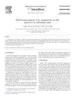
1
2
Trung T. Pham, Fr´ed´eric Joucken, Jessica Campos-Delgado, Benoit Hackens,
Jean-Pierre Raskin, Robert Sporken, Direct growth of graphitic carbon on
Si(111), Applied Physics Letters, 102, 013118 (2013).
Trung T. Pham, Jessica Campos-Delgado, Fr´ed´eric Joucken, Jean-Fran¸cois
Colomer, Benoit Hackens, Jean-Pierre Raskin, Cristiane N. Santos, Robert
Sporken, Direct growth of graphene on Si(111), Journal of Applied Physics,
115, 163106 (2014).
Number
Conference presentations
1
Trung T. Pham, Fr´ed´eric Joucken, Jessica Campos-Delgado, Benoit Hackens,
Jean-Pierre Raskin, Robert Sporken, Direct growth of graphitic carbon on
Si(111) by e-beam evaporation, poster presentation, Materials sciences and
technology, Halong-Vietnam (October 2012).
Trung T. Pham, Fr´ed´eric Joucken, Jessica Campos-Delgado, Benoit Hackens,
Jean-Pierre Raskin, Robert Sporken, Direct growth of nanocrystalline graphene
films on Si(111), poster presentation, Graphene2013, Bilbao-Spain (April 2013).
Trung T. Pham, Fr´ed´eric Joucken, Benoit Hackens, Jean-Pierre Raskin, Robert
Sporken, Direct growth of graphene on Si(111), oral presentation (invited talk),
MBE-grown graphene 2013, Berlin-Germany (October 2013).
Trung T. Pham, Fr´ed´eric Joucken, Jessica Campos-Delgado, Benoit Hackens,
Jean-Pierre Raskin, Robert Sporken, Direct growth of graphene on Si(111),
poster presentation, Graphene2014, Toulouse-France (May 2014).
Trung T. Pham, Fr´ed´eric Joucken, Cristiane N. Santos, Benoit Hackens, JeanPierre Raskin, Robert Sporken, Influence of substrate temperature and thickness
of SiC buffer layer on the quality of graphene on Si(111), poster presentation,
Graphene2015, Bilbao-Spain (March 2015).
Trung T. Pham, Fr´ed´eric Joucken, Cristiane N. Santos, Benoit Hackens, JeanPierre Raskin, Robert Sporken, Influence of substrate temperature and thickness
of SiC buffer layer on the quality of graphene on Si(111), oral presentation,
Graphene2015, Bilbao-Spain (March 2015).
2
3
4
5
6
vii
Epigraph
Learn from yesterday, live for today, hope for tomorrow. The important thing is not to
stop questioning.
Albert Einstein (1879 - 1955)
There are two possible outcomes:
❼ If the result confirms the hypothesis, then you’ve made a measurement.
❼ If the result is contrary to the hypothesis, then you’ve made a discovery.
Enrico Fermi (1901 - 1954)
viii
Table of Contents
1. INTRODUCTION . . . . . . . . . . . . . . . . . . . . . . . . . . . . . .
1
1.1. General introduction. . . . . . . . . . . . . . . . . . . . . . .
1
1.2. Outline . . . . . . . . . . . . . . . . . . . . . . . . . . . .
7
2. STRUCTURAL PROPERTIES, STUDIED METHOD AND EXPERIMENTAL TECHNIQUES . . . . . . . . . . . . . . . . . . . . . . . .
8
2.1. Introduction . . . . . . . . . . . . . . . . . . . . . . . . . .
8
2.2. Structure of C/Si(111) samples . . . . . . . . . . . . . . . . . .
8
2.3. Crystallographic structures of relevant materials . . . . . . . . . . .
9
2.3.1. Real and reciprocal lattice vectors . . . . . . . . . . . . . . . . . .
9
2.3.2. Reciprocal characterization . . . . . . . . . . . . . . . . . . . . . .
11
2.3.3. Crystallographic structure in the real and reciprocal space . . . . 12
a.
Si(111) 7×7 surface reconsctruction . . . . . . . . . . . . 12
b.
Silicon carbide . . . . . . . . . . . . . . . . . . . . . . . 14
c.
Amorphous carbon . . . . . . . . . . . . . . . . . . . . . 15
d.
Graphite - graphene . . . . . . . . . . . . . . . . . . . . 16
2.3.4. Summary . . . . . . . . . . . . . . . . . . . . . . . . . . . . . . . 19
2.4. Sample preparation . . . . . . . . . . . . . . . . . . . . . . .
19
2.4.1. Principle of e-beam evaporation . . . . . . . . . . . . . . . . . . . 19
a.
Evaporation and deposition rates . . . . . . . . . . . . . 20
b.
Evaporation sources . . . . . . . . . . . . . . . . . . . . 23
c.
Evaporation materials . . . . . . . . . . . . . . . . . . . 24
d.
E-beam power and deposition rate . . . . . . . . . . . . 24
e.
Advantages and disadvantages . . . . . . . . . . . . . . . 24
2.4.2. Experimental setup . . . . . . . . . . . . . . . . . . . . . . . . . . 25
ix
a.
Main components needed to setup the experiment using
graphite rod form of evaporation . . . . . . . . . . . . . 25
b.
Principle of operation . . . . . . . . . . . . . . . . . . . 26
c.
Experimental conditions for carbon evaporation . . . . .
27
2.5. Experimental techniques . . . . . . . . . . . . . . . . . . . . .
28
2.5.1. Ultra-high vacuum . . . . . . . . . . . . . . . . . . . . . . . . . . 28
2.5.2. Low energy electron diffraction (LEED) and reflection high energy
electron diffraction (RHEED) . . . . . . . . . . . . . . . . . . . . 29
a.
Principle of LEED and RHEED . . . . . . . . . . . . . . 29
b.
LEED geometry . . . . . . . . . . . . . . . . . . . . . .
31
c.
RHEED geometry . . . . . . . . . . . . . . . . . . . . .
31
2.5.3. Auger electron (AE) and X-ray photoelectron (XP) spectroscopies 38
a.
Principle of AES and XPS . . . . . . . . . . . . . . . . . 38
b.
Depth profiling of AES and XPS . . . . . . . . . . . . . 40
2.5.4. Raman spectroscopy (RS) . . . . . . . . . . . . . . . . . . . . . .
41
a.
Principle of Raman . . . . . . . . . . . . . . . . . . . . .
41
b.
Raman for graphene . . . . . . . . . . . . . . . . . . . . 43
2.5.5. Scanning tunneling microscopy (STM) and atomic force microscopy
(AFM) . . . . . . . . . . . . . . . . . . . . . . . . . . . . . . . . . 45
a.
STM principle . . . . . . . . . . . . . . . . . . . . . . . 45
b.
Mode of operation . . . . . . . . . . . . . . . . . . . . . 46
c.
AFM principle . . . . . . . . . . . . . . . . . . . . . . . 47
d.
Mode of operation . . . . . . . . . . . . . . . . . . . . . 48
2.6. Summary . . . . . . . . . . . . . . . . . . . . . . . . . . .
3. GROWING GRAPHENE ON Si: STATE OF THE ART . . . . . .
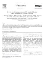
49
50
3.1. Introduction . . . . . . . . . . . . . . . . . . . . . . . . . .
50
3.2. Electron beam evaporators . . . . . . . . . . . . . . . . . . . .
50
3.3. MBE growth . . . . . . . . . . . . . . . . . . . . . . . . . .
52
3.4. CVD growth . . . . . . . . . . . . . . . . . . . . . . . . . .
56
3.5. Laser irradiation . . . . . . . . . . . . . . . . . . . . . . . .
61
x
3.6. Transfer processes . . . . . . . . . . . . . . . . . . . . . . . .
62
3.7. Summary . . . . . . . . . . . . . . . . . . . . . . . . . . .
64
4. EXPERIMENTAL RESULTS AND DISCUSSION . . . . . . . . . .
65
4.1. Introduction . . . . . . . . . . . . . . . . . . . . . . . . . .
65
4.2. Preparation of Si(111) 7×7 substrate . . . . . . . . . . . . . . . .
65
4.3. Growing graphene on Si(111) 7×7 substrate . . . . . . . . . . . . .
67
4.3.1. Experimental details . . . . . . . . . . . . . . . . . . . . . . . . .
67
4.3.2. Proposed structural models for direct deposition of carbon layers . 69
a.
Model 1: C/a-C/Si(111) . . . . . . . . . . . . . . . . . . 69
b.
Model 2: C/a-C/3C -SiC/Si(111) . . . . . . . . . . . . . 74
c.
Model 3: C/3C -SiC/Si(111) . . . . . . . . . . . . . . . . 80
d.
Model 4: C/Si/3C -SiC/Si(111) . . . . . . . . . . . . . . 90
4.3.3. Summary . . . . . . . . . . . . . . . . . . . . . . . . . . . . . . . 99
4.3.4. Discussion . . . . . . . . . . . . . . . . . . . . . . . . . . . . . . . 99
a.
Basics of diffusion . . . . . . . . . . . . . . . . . . . . . 100
b.
Phenomenological approach . . . . . . . . . . . . . . . . 100
c.
Diffusion coefficient . . . . . . . . . . . . . . . . . . . . . 102
d.
Silicon diffusion through 3C -SiC buffer . . . . . . . . . . 103
4.4. Summary . . . . . . . . . . . . . . . . . . . . . . . . . . . 108
5. CONCLUSION . . . . . . . . . . . . . . . . . . . . . . . . . . . . . . . 110
5.1. Summary of the results. . . . . . . . . . . . . . . . . . . . . . 110
5.2. Perspectives . . . . . . . . . . . . . . . . . . . . . . . . . . 112
Bibliography . . . . . . . . . . . . . . . . . . . . . . . . . . . . . . . . . . . 114
xi
List of Figures
1.1. (a) Carbon family tree shows known carbon allotropes where graphene
is illustrated as the origin of all graphitic forms: roll into fullerenes
(buckyballs)/ nanotubes or stack into multilayer graphite; (b) A sp2
hybridization bonds in the honeycomb structure. Images adapted from
Refs. [5, 6]. . . . . . . . . . . . . . . . . . . . . . . . . . . . . . . . . . .
1
1.2. (a) Number of graphene publications vs. year (Source from wwww.google.com
when searching for “number of publications in graphene”); (b) number
of published patents in graphene until 2014 (Source from the worldwide
patent landscape in 2015). The data for 2013 and 2014 is shaded light
blue to show the quick change over the period with the peak year as shown
in 2014. . . . . . . . . . . . . . . . . . . . . . . . . . . . . . . . . . . . . 3
1.3. Quality vs. Cost for graphene production. Reported by Novoselov et al.
[45].
(1) CVD growth: high graphene quality, low cost. Used for applications
such as coating, bio, transparent conductive layers, electronics, photonics;
(2) Mechanical exfoliation: high graphene quality, high cost. Used for
research and prototyping;
(3) SiC graphitization: high graphene quality, high cost. Used for electronics, RF transistors;
(4) Molecular assembly: high graphene quality, high cost. Preferred for
nanoelectronics;
(5) Liquid-phase exfoliation: low quality, low cost, for applications such as
coating, composites, inks, energy storage, bio, transparent conductive layers.
4
1.4. (a) Realization of multifunctional graphene on Si utilizing different crystallographic orientations of Si substrate, adapted from [67]; (b) Terahertz
emission in graphene on 3C -SiC/Si(110), adapted from [68]; (c) G-FET
on 3C -SiC/Si(111), adapted from [69]. . . . . . . . . . . . . . . . . . . .
6
2.1. Structural model for growing graphene on Si(111) 7×7 substrate. . . . .
9
2.2. The relationship between a real and reciprocal lattice vectors. . . . . . . 10
2.3. Electron diffraction from two parallel planes. . . . . . . . . . . . . . . . .
xii
11
2.4. (a) Side view of single crystalline network of silicon atoms on Si(111); (b)
(7×7) unit cell obtained by repeating the primitive unit cell (dashed rhombus in red) and (c) top view of Si(111) surface after surface reconstruction.
Images adapted from Ref. [82]. . . . . . . . . . . . . . . . . . . . . . . . 12
2.5. (a) Top view along [111] of the DAS model of the Si(111) 7×7 reconstructed
surface by Takayanagi et al. [83]. The rhomboidal surface unit cells consist
of faulted and unfaulted half cells, separated by rows of dimers. There
are 12 adatoms in the topmost Si layer (layer 0 - indicated with C at
corner sites and E at edge center sites) + 6 rest atoms in layer 2 (marked
with a + sign) + a corner hole atoms in layer 3 = 19 in the (7Ö7)
reconstructed surface unit cell. The unit cell vectors along [110] and its
corresponding reciprocal lattice; (b) The unit cell vectors along [112] and
its corresponding reciprocal lattice. Images adapted from Ref. [84]. . . . 13
2.6. (a) The building block of SiC - tetrahedron of C atom bonded to four Si
atoms; Stacking of layers in real space compared among (b) 3C -, (c) 6H -,
and (d) 4H -SiC. . . . . . . . . . . . . . . . . . . . . . . . . . . . . . . . . 14
2.7. (a) Top view along [0001] of the real space from three common SiC
polytypes; (b) corresponding reciprocal lattice. . . . . . . . . . . . . . . . 15
2.8. Model of the 64 atom ta-C network with 22 three-fold coordinated atoms
(sp2 hybridized) (dark spheres) and 42 four-fold coordinated atoms (sp3
hybridized) (light spheres). Figure adapted from Ref. [92]. . . . . . . . . 16
2.9. (a) Hexagonal and (b) Rhombohedral lattice of graphite with different
types of stacking order. Figures (a) and (b) adapted from Ref. [93]. . . . 17
2.10. (a) The sp2 bonds of (b) Graphene lattice in real space with two lattice
vectors a1 and a2 ; (c) Sketch of the first Brillouin zone in the reciprocal
lattice: (d) The electronic band structure of graphene. Images (a) adapted
from Ref. [94] and (d) adapted from Ref. [95]. . . . . . . . . . . . . . . . 18
2.11. Flow diagram of physical vapor deposition. . . . . . . . . . . . . . . . . . 20
2.12. Geometry of carbon evaporation. . . . . . . . . . . . . . . . . . . . . . . 22
2.13. Main components of our e-beam evaporator. . . . . . . . . . . . . . . . . 25
2.14. (a) A simulation process for carbon evaporation from the graphite rod
form (Source from Tectra company [115]; (b) The ratio between deposition
rate and ion current as a function of the heating power were measured
at the position d ∼ 10 cm, HV = 1.5 - 1.6 kV, IF = 8 A and Ie = 60
- 80 mA with the vapour pressure ∼ 10−5 - 10−4 mbar calculated using
equation (2.22) (the gauge reading pressures ≤ 6.0 × 10⁻⁸ mbar). . . . . 26
2.15. Electron diffraction in the case of LEED with incident electron beam
normal to the surface (ki and kf are the incident wavevector and the
scattered wavevector, respectively). . . . . . . . . . . . . . . . . . . . . . 29
xiii
2.16. (a) Real and reciprocal space of electron diffraction (G is the reciprocal
lattice vector which is related to ki and kf as section 2.3.2). The spots
induced by the diffraction beams are labelled by (00), (01), etc.; (b) LEED
pattern of Si(111) 7×7 surface reconstruction at 38 eV. . . . . . . . . . . 30
2.17. (a) A typical RHEED geometry with a description of the intersection
between the Ewald sphere and the reciprocal lattice rods; (b) RHEED
patterns of Si(111) 7×7 surface reconstruction with an e-beam along
different directions from corresponding reciprocal lattices as constructed
in section 2.3.3.a. Images adapted from Ref. [121]. . . . . . . . . . . . . .
31
2.18. Schematic of electron scattering geometry on single crystalline film with
smooth surface. . . . . . . . . . . . . . . . . . . . . . . . . . . . . . . . . 32
2.19. Schematic of electron scattering geometry on single crystalline film with
islands. . . . . . . . . . . . . . . . . . . . . . . . . . . . . . . . . . . . . . 33
2.20. Schematic of electron scattering geometry on polycrystalline film. . . . . 34
2.21. Graphical representation of the scattering vector. . . . . . . . . . . . . . 35
2.22. (a) A construction of RHEED geometry for determining the lattice constant of a single crystalline films; (b) RHEED pattern of 3C -SiC formation
on Si(111). Image (a) adapted from Ref. [124]. . . . . . . . . . . . . . . . 37
2.23. A typical RHEED pattern of polycrystalline graphene on Si(111). . . . . 38
2.24. The mechanism of AES and XPS processes. . . . . . . . . . . . . . . . . 39
2.25. (a) AES and (b) XPS C 1s core level spectra of graphene on Si(111). . . 40
2.26. The schematic diagram for determining the depth of AES and XPS
processes . . . . . . . . . . . . . . . . . . . . . . . . . . . . . . . . . . .
41
2.27. (a) Model of Raman effect which is caused by inelastic light scattering
(Stokes and anti-Stokes); (b) Various vibrational modes from carbon atoms
in a typical graphene lattice of free-defects. Figure (b) adapted from Ref.
[125]. . . . . . . . . . . . . . . . . . . . . . . . . . . . . . . . . . . . . . . 42
2.28. (a) Schematic of atomically sharp tip and electronic connection; (b) The
tunneling current It as a function of the distance Z between STM tip and
sample surface; (c) A schematic of line by line scanning from top to bottom;
Atomic resolution STM images of Si(111) 7×7 surface reconstruction with
(d) empty (Vt =1.7 V) with 6 adatoms per triangle and (e) filled (Vt =1.7 V) electronic states of the surface (with rest/adatoms of stacking fault
appearing brighter in a solid purple triangle). Images (a) and (b) adapted
from Ref. [135]; (d) and (e) adapted from Ref. [136]. . . . . . . . . . . . 46
2.29. (a) Schematic of AFM mechanism and (b) Force F as a function of
tip-sample separation Z [139]. The image (a) adapted from Ref. [140]. . 48
xiv
3.1. RHEED patterns of pure Si(111) with a coverage of ∼ 20 nm of undoped-Si
(a) and after carbon deposition at 560 ➦C (b), 600 ➦C (c), 660 ➦C (d), 700
➦C (e) and 560 ➦C followed by annealing at 830 ➦C (f). Images adapted
from Ref. [54]. . . . . . . . . . . . . . . . . . . . . . . . . . . . . . . . . .
51
3.2. (a) XPS spectra of C 1s core level and (b) Raman spectra (Source from
Ref. [54]); (c) Raman spectra and (d) Near edge X-ray absorption fine
structure (NEXAFS) at various sample temperatures (Source from Ref.
[55]). . . . . . . . . . . . . . . . . . . . . . . . . . . . . . . . . . . . . . .
51
3.3. Crystallinity of the 3C -SiC film grown on Si(100) substrate in the T-P
diagram where the circles, triangles and crosses denote single-crystalline,
poly-crystalline and amorphous films, respectively. Image adapted from
Ref. [62]. . . . . . . . . . . . . . . . . . . . . . . . . . . . . . . . . . . . . 53
3.4. (a) Comparison of the Raman spectra of epitaxial graphene on 3C SiC/Si(111) (bottom), 3C -SiC/Si(100) (middle) and 3C -SiC/Si(110) (top)
together with corresponding TEM images of graphene layers. Image
adapted from Ref. [62]; (b) Raman spectra of graphene formed on 3C SiC/AlN/Si(111) with and without surface treatments. Image adapted
from Ref. [75]. . . . . . . . . . . . . . . . . . . . . . . . . . . . . . . . . . 54
3.5. Raman measurements: (a) Time evolution of epitaxial graphene, (b) The
grain size (La) vs. the annealing time of graphitization. Images adapted
from Ref. [148]. . . . . . . . . . . . . . . . . . . . . . . . . . . . . . . . . 56
3.6. Raman spectra of bulk graphite, untreated 3C -SiC/Si (111) substrate,
samples annealed at 1125, 1225, 1300, 1325 and 1375 ➦C (bottom-to-top)
for 10 min. Figure adapted from Ref. [63]. . . . . . . . . . . . . . . . . . 57
3.7. STM images of graphene on 3C -SiC/Si(111) after annealing at 1300 ➦C:
(a) 20 × 20 nm➨ with wrinkles (VS = 70 mV, IT = 0.3 nA); (b) and (c)
Moir´e pattern with
symmetry (VS = 50 mV, IT = 0.2 nA). A
√ hexagonal
√
blue insert is a (6 3 × 6 3)R30➦ unit cell. Images adapted from Ref. [63]. 58
3.8. (a) FT-IR spectra of the carburized Si(110) substrate at various annealing temperatures; (b) Raman spectra of 3C -SiC/Si(110) before and
after graphene formation at 1100 ➦C; (c) High-resolution TEM image of
graphene/3C -SiC/Si(110) structure. Images adapted from Ref. [150]. . . 59
3.9. (a) Raman spectra of AlN/Si(111) templates after graphene growth; (b)
AFM images of AlN/Si(111) after annealing at 1150 ➦C; After graphene
growth at 1150 ➦C (c), 1250 ➦C (d) and 1350 ➦C (e). Images adapted from
Ref. [153]. . . . . . . . . . . . . . . . . . . . . . . . . . . . . . . . . . . . 60
3.10. Raman spectra of graphene on Si wafers by using various catalysts were
reported by Lee et al. [65] (a), Park et al. [50] (b), Liu et al. [155] (c)
and Howsare et al. [66] (d). . . . . . . . . . . . . . . . . . . . . . . . . .
xv
61
3.11. (a) SEM image of laser processed Si surface and (b) a magnified SEM
image of the center of the laser irradiated area; (c) Raman spectra recorded
from the central area. Images adapted from Ref. [61]. . . . . . . . . . . . 62
3.12. (a) Direct exfoliation from HOPG on Si(111) 7×7 surface reconstruction
by means of a wobble stick in UHV, adapted from Ref. [64] and the
preparation steps of graphene on Si(111) heterojunctions with hydrogen
and methyl termination of the silicon surface prior to the graphene transfer,
adapted from Ref. [158]. . . . . . . . . . . . . . . . . . . . . . . . . . . . 63
4.1. AES spectra of untreated silicon (dark cyan) and after Ar+ sputtering,
followed by annealing up to ∼ 1050 ➦C (gray). Without Ar+ sputtering,
AES spectrum of clean Si surface shows similar results after annealing. . 66
4.2. (a) LEED pattern at 57 eV, (b) STM image of Si(111) surface on an area of
200×200 nm2 (VS = +3 V, IT = 0.25 A) with an inset of atomic resolution
((VS = +2 V, IT = 0.2 A)) and (c) height profile of corresponding STM
images. The sample was prepared by Ar+ sputtering before annealing.
By doing this way, we often found steps after annealing. . . . . . . . . .
67
4.3. Si and C sources in the UHV chamber. . . . . . . . . . . . . . . . . . . . 68
4.4. A growth process for graphene formation on Si(111) 7×7 substrate where
C stands for carbon source ON. The Si(111) substrates were cleaned by
Ar+ sputtering, followed by annealing up to ∼ 1050 ➦C as mentioned in
section 4.2. . . . . . . . . . . . . . . . . . . . . . . . . . . . . . . . . . . 70
4.5. (a) AES spectra around the CKLL transition of the four samples as well as
HOPG and SiC; (b) The differentiated spectra; (c) C 1s XPS spectra of
samples #1 to #4 (and HOPG and SiC as references); (d) LEED pattern
at 50.2 eV of sample #1 showing spots corresponding to the SiC formation
(lattice constant of ∼ 3.1 Å). . . . . . . . . . . . . . . . . . . . . . . . . .
71
4.6. Raman measurements of the studied samples, the different spectra have
been vertically shifted to better illustrate the differences. The different
peaks appearing in the spectra of samples #2, #3 and #4 have been
fitted to single Lorentzians. . . . . . . . . . . . . . . . . . . . . . . . . . 72
4.7. STM images of samples #2, #3 and #4. a) Large scale (400×400 nm2 )
image of sample #4 with a height profile (VSample = +3 V, IT unnel =
0.35 nA); b) 2.5×2.5 nm2 image of sample #2 (VS = −1 V, IT = 6 nA; c)
1×1 nm2 image of sample #3 (VS = −1.5 V, IT = 4 nA; d) 2.5×1.5 nm2
image of sample #4 (VS = −1 V, IT = 4 nA) showing the honeycomb
lattice of a graphene sheet. . . . . . . . . . . . . . . . . . . . . . . . . . . 74
xvi
4.8. A growth process for graphene formation on Si(111) 7×7 substrate where
Si and C stand for silicon and carbon sources ON, respectively. The
Si(111) substrates were cleaned by direct annealing up to ∼ 1050 ➦C as
mentioned in section 4.2. . . . . . . . . . . . . . . . . . . . . . . . . . . . 75
4.9. RHEED patterns of the respective samples under various growth times
on Si(111). . . . . . . . . . . . . . . . . . . . . . . . . . . . . . . . . . . . 76
4.10. (a) AES spectra around the CKLL transition of SiC growth and after
carbon deposition on top of SiC layers (samples #1 → #4); (b) Differentiated spectra with respect to the kinetic energy; (c) C 1s and (d) Si 2p
XPS spectra of corresponding samples (pure Si(111), HOPG and SiC as
references). . . . . . . . . . . . . . . . . . . . . . . . . . . . . . . . . . .
77
4.11. Raman measurements for different studied samples #1, #2, #3, and #4.
78
4.12. STM images of sample #4 (a) 1ì1 àm2 (VSample = +4.0 V, IT unnel =
0.6 nA) after SiC growth and (b) 1ì1 àm2 (VSample = +4.0 V, IT unnel =
0.35 nA) after graphene formation on top by more carbon deposition at
the substrate temperature of 1000 ➦C; (c) 80×80 ˚
A2 (VS = −0.1 V, IT =
2
A (VS = −0.1 V, IT = 10 nA) showing atomic
10 nA) and (d) 35×35 ˚
resolution of the AB stacking order in the graphene hexagonal lattice. . . 80
4.13. Schematic of atomic arrangements of graphene and 3C -SiC/Si(111) in
real space. Image adapted from Ref. [170]. . . . . . . . . . . . . . . . . .
81
4.14. Direct deposition of carbon atoms on 3C -SiC/Si(111) where Si and C stand
for silicon and carbon sources ON, respectively. The Si(111) substrates
were cleaned by direct annealing up to ∼ 1050 ➦C as mentioned in section
4.2. . . . . . . . . . . . . . . . . . . . . . . . . . . . . . . . . . . . . . . .
81
4.15. RHEED patterns of the respective samples under various growth times
on Si(111). . . . . . . . . . . . . . . . . . . . . . . . . . . . . . . . . . . . 82
4.16. (a) AES spectra around the CKLL transition of the five different samples;
(b) AES spectra, differentiated with respect to kinetic energy; (c) C 1s
and (d) Si 2p XPS spectra of samples #1 to #5 (pure Si(111), HOPG
and SiC as references). . . . . . . . . . . . . . . . . . . . . . . . . . . . . 84
4.17. (a) Raman measurements recorded at λ = 514 nm (Elaser = 2.41 eV)
of samples #2, #3, #4, #5, MWCNTs and CVD-produced single layer
graphene; (b) corresponding intensity ratios; (c) FWHM of D and 2D
bands and (d) crystal size of the measured samples derived from the ID /IG
ratios. . . . . . . . . . . . . . . . . . . . . . . . . . . . . . . . . . . . . . 85
4.18. Maps of I2D /IG (left), ID /IG (center) intensity ratios and corresponding
optical images (right, scale bar 10 µm). . . . . . . . . . . . . . . . . . . . 87
xvii
4.19. (a) HR-SEM images showing the surface morphology and (b) a zoom-in on
the square area of sample #5 observing surface structure like 3D porous
network; (c) Surface topographic AFM images of sample #4 and (d) the
corresponding phase image. . . . . . . . . . . . . . . . . . . . . . . . . . 88
4.20. STM images of sample #5 (a) 4×4 µm2 (VSample = +5.5 V, IT unnel =
0.45 nA); (b) 100×100 ˚
A2 (VS = −0.12 V, IT = 10 nA) with a corresponding FFT image in the inset that exhibits diffraction pattern of
hexagonal film structure; (c) 70×70 ˚
A2 (VS = −0.12 V, IT = 10 nA); (d)
30×30 ˚
A2 (VS = −0.12 V, IT = 10 nA) showing the honeycomb lattice of
a graphene sheet. . . . . . . . . . . . . . . . . . . . . . . . . . . . . . . . 89
4.21. (a) Schematic diagram and (b) growth process for graphene formation
on Si(111) 7×7 substrate where Si and C stand for silicon and carbon
sources ON, respectively. The Si(111) substrates were cleaned by direct
annealing up to ∼ 1050 ➦C as mentioned in section 4.2. . . . . . . . . . .
91
4.22. (a) AES spectra around the SiLVV and CKLL transitions of the seven
different samples as well as HOPG, bulk SiC and Si(111) as references;
(b) The differentiated spectra. The dotted ellipse in the magnified CKLL
spectra shows the region where features from SiC are located . . . . . . . 92
4.23. (a) C 1s and (b) Si 2p XPS spectra of samples #1 to #7 (HOPG, Si face
of bulk 6H -SiC and Si(111) used as references). . . . . . . . . . . . . . . 93
4.24. Model used for the calculation of number of graphene layers on 3C SiC/Si(111) substrate. . . . . . . . . . . . . . . . . . . . . . . . . . . . . 95
4.25. (a) Raman measurements recorded at λ = 514 nm (Elaser = 2.41 eV)
of samples #1, #2, #3, #4, #7, pure Si(111), 6H -SiC and HOPG as
references; (b) Intensity maps of ID , IG , I2D , ID /IG , and I2D /IG on
30 ì 30 àm2 from samples #4 and #7 (scale bar 5 µm). . . . . . . . . 96
4.26. (a) SEM image of sample #2 and its STM images (b) 200×200 nm2
(VSample = +3.0 V, IT unnel = 0.35 nA); (c) 30×30 ˚
A2 (VS = −1.4 V, IT =
30 nA); and (d) SEM image of sample #7 and its corresponding STM
images (e) 200×200 nm2 (VS = +5.0 V, IT = 0.35 nA); (f) 30×30 ˚
A2
(VS = −0.2 V, IT = 25 nA) showing the atomic resolution of the AB
stacking order of a typical graphene lattice. . . . . . . . . . . . . . . . . . 98
4.27. Schematic diagram of the local concentration and diffusion flux through a
unit area (A) at position x. . . . . . . . . . . . . . . . . . . . . . . . . . 101
4.28. (a) Dependence of the diffusion coefficient D on the growth temperature
T from equation (4.10) and (b) data is transformed in lnD vs. 1/T. . . . 103
xviii
4.29. Schematic diagram of interface between Si(111) substrate and 3C -SiC
buffer layer. (a) Assuming that the sample with an abrupt interface (ideal
case) is heated immediately at 1100 ➦C and (c) is described in T vs. t;
(b, d) after SiC growth on Si(111) at 1000 ➦C (realistic case), followed by
slow annealing up to 1100 ➦C for 2 hours as illustrated by orange solid
line in T vs. t. . . . . . . . . . . . . . . . . . . . . . . . . . . . . . . . . . 104
4.30. LEED patterns at 57 eV of the Si(111) substrate (a), after ∼ 19-nm-thick
3C -SiC on Si(111) (b) and after 2 hours annealing at 1100 ➦C (c). . . . . 105
4.31. (a) XPS depth profile of concentration of Si atoms CSi in SiC buffer layers
vs. sputtering time, measured before annealing (C0 ∼ 52.0% Si and ∼
43.0% C); (b) Concentration of Si atoms CSi vs. sputtering time from
the sample surface after annealing a ∼ 19-nm-thick 3C-SiC on Si(111) at
1100 ➦C. . . . . . . . . . . . . . . . . . . . . . . . . . . . . . . . . . . . . 106
4.32. Fit of equation (4.12) to measured Si concentration profile for determining
the diffusion coefficient D of Si. . . . . . . . . . . . . . . . . . . . . . . . 107
xix
List of Tables
1.1. Properties of carbon materials in comparison with silicon. (*) measured
from 270 K to 3 K, respectively; (**) graphene on SiO2 (the value was
independent of temperature T between 10 and 100 K); (***) graphene on
4H -SiC measured at ∼ 0.3 K; (****) suspended graphene measured at ∼
5 K. . . . . . . . . . . . . . . . . . . . . . . . . . . . . . . . . . . . . . .
2
2.1. The most three common polytypes of SiC and their structural properties,
reported by Hmida et al. [85]. . . . . . . . . . . . . . . . . . . . . . . . . 15
2.2. A list of the special points in the Brillouin zone along with their associated
vector in k-space. The Γ point is referred to as the zone center. . . . . . 19
2.3. Structural properties of relevant materials; d.c. is diamond cubic, hex. is
hexagonal and rhom. is rhombohedral. . . . . . . . . . . . . . . . . . . . 19
4.1. Values of D (cf. Fig. 4.5 (b) for the four samples, SiC and HOPG (in eV) 70
4.2. ID /IG and I2D /IG ratios and average domain size of corresponding samples
derived from the ID /IG ratio. . . . . . . . . . . . . . . . . . . . . . . . . 79
4.3. Expected (Ge ) and measured (Gm ) ring radii. The expected radii are
computed using a lattice constant of 2.46 ˚
A for graphene films. . . . . . . 83
4.4. Summary of the ratio ICG /ICSiC for different studied samples. . . . . . . . 94
4.5. ID /IG and I2D /IG ratios from different samples for comparison and average
domain size derived from the ID /IG ratio. . . . . . . . . . . . . . . . . .
97
4.6. Summary of main parameters among four different studied models. . . . 99
4.7. The flux and atomic percentage of diffusing Si across different thicknesses
of SiC buffer layer after 2 hours of annealing at 1100 ➦C using Cs ∼ 5.0 ×
1022 atoms/cm3 in the bulk Si(111) and C0 ∼ 4.8 × 10²² atoms/cm3 in
3C -SiC. Atomic percentage of Si is calculated with respect to the flux of
deposited carbon ∼ 1.2 × 10¹³ atoms/cm2 · s. . . . . . . . . . . . . . . . . 108
xx
Chapter 1
INTRODUCTION
1.1. General introduction
Carbon is a chemical element at the origin of living things. It exists in many different
allotropes with different kinds of hybridization such as sp3 (as in diamond), sp2 (as in
graphite), sp (as in carbynes) [1, 2]. During the last few decades, it has always surprised
the scientific community with the discovery of new materials which are derived from
carbon such as fullerene (0D) in 1985 [3], carbon nanotube (1D) in 1991 [4] and graphene
(2D).
Fig. 1.1: (a) Carbon family tree shows known carbon allotropes where graphene is
illustrated as the origin of all graphitic forms: roll into fullerenes (buckyballs)/ nanotubes
or stack into multilayer graphite; (b) A sp2 hybridization bonds in the honeycomb
structure. Images adapted from Refs. [5, 6].
1
Among them, graphene is the newest member of the carbon family. It was isolated and
its electronic transport properties were first measured in 2004 [7]. It consists of a single
layer of sp2 bonded carbon atoms in a two-dimensional honeycomb crystal lattice. As
described in Fig. 1.1, graphene is considered as the basic building block of all graphitic
forms [5].
As illustrated by Geim et al. [5], graphene can roll into buckyballs (0D) or nanotubes (1D)
as well as stack into multilayer graphite (3D). These materials have unusual properties
compared to silicon (Table 1.1).
Properties
Silicon
Fullerenes
Carbon nanotubes
Electrical conductivity
∼ 108 (SWCNTs) [10];
−4
−5
∼ 4.3 × 10 [8] ∼ 2×10 [9]
(Ω−1 · m−1 )
3 ×10⁶ (MWCNTs) [11]
Thermal conductivity
6.6 × 10⁴ (SWCNTs) [16];
156 [14]
0.4 [15]
(W/m K)
> 3 × 10³ (MWCNTs) [17]
Optical transparency
(%)
Electron mobility µ
(cm2 /V·s)
≤ 1.4 × 10³ [22]
0.56 [23]
∼ 105 [24]
HOPG
3
Graphene
∼ 2.6 × 10 [12]
∼ 1.3 × 10⁸ [13]
∼ 3 × 10³ [18, 19]
∼ 5 × 10³ [20]
-
∼ 97.7 [21]
∼ 1.5 × 10⁴ (**) [26],
5ì104 à 4 ì 107 (*) [25] ≥ 1.1 × 10⁴ (***) [27];
∼ 2.0 × 10⁵ (****) [28]
Table 1.1: Properties of carbon materials in comparison with silicon. (*) measured
from 270 K to 3 K, respectively; (**) graphene on SiO2 (the value was independent of
temperature T between 10 and 100 K); (***) graphene on 4H -SiC measured at ∼ 0.3 K;
(****) suspended graphene measured at ∼ 5 K.
In a graphene lattice, carbon atoms form a very strong σ bond with the three other
atoms through sp2 hybridization in the same plane (Fig. 1.1 (b)). This is responsible for
the mechanical properties of graphene [29] while the remaining p orbital is available to
form a π bond with adjacent atoms in the surface normal, which gives rise to graphene’s
unique electronic properties [7, 26, 30]. This has brought graphene to the center of
attention during the past ten years. Indeed, graphene exhibits ballistic electron transport
(electrons can travel submicron distances without scattering) [5], very high electron
mobilities have been observed (∼ 15000 cm2 /V.s for graphene on SiO2 substrate [26],
≥ 11000 cm2 /V.s for epitaxial graphene on 4H -SiC substrate at ∼ 0.3 K [27] and
∼ 200000 cm2 /V.s for suspended graphene at ∼ 5 K [28]). Moreover, some studies
also reported other outstanding properties such as high transparency [21] and superior
thermal conductivity [20] which make graphene emerge as an exciting novel material.
Therefore, graphene was considered as an excellent candidate for nanoelectronic devices.
For example, graphene field-effect transistors (G-FETs) [31], transparent electrodes in
solar cells [32], light emitting diodes [33], optoelectronics [34], sensors [35] and so on.
2
Since the discovery of isolated graphene by Geim and his co-workers at Manchester
University using mechanical exfoliation of highly oriented pyrolytic graphite (HOPG) [7],
followed by the award of the Nobel prize in Physics 2010 [36], enormous efforts have been
devoted to grow, transfer and characterize graphene on various substrates using many
different methods in order to obtain high quality and large area graphene as reflected
by number of publications and published patents per year from the worldwide patent
landscape in 2015 (Fig. 1.2).
Fig. 1.2: (a) Number of graphene publications vs. year (Source from wwww.google.com
when searching for “number of publications in graphene”); (b) number of published
patents in graphene until 2014 (Source from the worldwide patent landscape in 2015).
The data for 2013 and 2014 is shaded light blue to show the quick change over the period
with the peak year as shown in 2014.
In fact, information about how graphene was prepared is very important because the
properties of graphene strongly depend on preparation methods [37]. In my opinion, the
reported methods generally fit into two major approaches which are
❼ Top-down
Some typical examples for this approach (exfoliation from bulk) are graphene
exfoliated from HOPG [7] or obtained by chemical exfoliation of pristine graphite
oxide [38]. Graphene oxide (GO) is produced from purified natural graphite by
the Hummers method [39, 40]. Moreover, one can also mention some others such
3
as liquid-phase exfoliation [41], chemical self assembly of graphene sheets from
graphite via electrostatic interactions [42], electrochemical exfoliation [43] and
graphite intercalation compounds (as stacks of individual doped graphene layers)
[44].
One can see that the advantages of these methods are scalability and high graphene
quality. However, it is difficult to obtain single layer of defect-free graphene because
of film impurity and large numbers of defects created during exfoliation and cost
for mass-production is very high (see Fig. 1.3).
Fig. 1.3: Quality vs. Cost for graphene production. Reported by Novoselov et al. [45].
(1) CVD growth: high graphene quality, low cost. Used for applications such as coating,
bio, transparent conductive layers, electronics, photonics;
(2) Mechanical exfoliation: high graphene quality, high cost. Used for research and
prototyping;
(3) SiC graphitization: high graphene quality, high cost. Used for electronics, RF
transistors;
(4) Molecular assembly: high graphene quality, high cost. Preferred for nanoelectronics;
(5) Liquid-phase exfoliation: low quality, low cost, for applications such as coating,
composites, inks, energy storage, bio, transparent conductive layers.
In particular, reduction of GO into graphene-like sheets by removing the oxygen
4