Tài liệu Cryptographic Algorithms on Reconfigurable Hardware- P11 docx
Bạn đang xem bản rút gọn của tài liệu. Xem và tải ngay bản đầy đủ của tài liệu tại đây (1.36 MB, 30 trang )
IN-
9.5 AES Implementations on FPGAs 279
- S-BOX
-INV S-BOX
Ml
lAF
AF
Ml
E/D
lAF
V
Ml
AF
S-BOX
-> INV S-BOX
b)
Fig. 9.26.
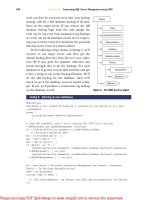
S-Box
and Inv
S-Box
Using (a) Different MI (b) Same MI
transformation (AF). For decryption, inverse affine transformation (lAF) is
applied first followed by MI step. Implementing MI as look-up table requires
memory modules, therefore, a separated implementation of BS/IBS causes the
allocation of high memory requirements especially for a fully pipelined archi-
tecture. We can reduce such requirements by developing a single data path
which uses one MI block for encryption and decryption. Figure 9.26 shows the
BS/IBS implementation using single block for MI.
There are two design approaches for implementing MI: look-up table
method and composite field calculation.
MI Using Look-Up Table Method
MI can be implemented using memory modules (BRAMs) of FPGAs by stor-
ing pre-computed values of MI. By configuring a dual port BRAM into two
single port BRAMs, 8 BRAMs are required for one stage of a pipeline ar-
chitecture, hence a total of 80 BRAMs are used for 10 stages. A separated
implementation of AF and lAF is made. Data path selection for encryption
and decryption is performed by using two multiplexers which are switched de-
pending on the E/D signal. A complete description of this approach is shown
in Figure 9.27
The data path for both encryption and decryption is, therefore, as follows:
Encryption: MI-> AF-> SR-> MC-^ ARK
Decryption: ISR-> IAF-> MI-^ IMC->IARK
The design targets Xilinx VirtexE FPGA devices (XCV2600) and occupies
80 BRAMs (43%), 386 I/O blocks (48%), and 5677 CLB sHces (22.3%). It runs
at 30 MHz and data is processed at 3840 Mbits/s.
Please purchase PDF Split-Merge on www.verypdf.com to remove this watermark.
280 9. Architectural Designs For the Advanced Encryption Standard
ISR
lAF
r— E/D
Ml
Ml using
look-up tables
AF
SR
IMC
lARK
MC
ARK
V
Fig. 9.27. Data Path
for
Encryption/Decryption
The data blocks
are
accepted
at
each clock cycle
and
then after
11 cy-
cles,
output encrypted/decrypted blocks appear
at the
output
at
consecutive
clock cycles.
It is an
efficient fully pipeline encryptor/decryptor core
for
those
cryptographic applications where time factor really matters.
MI with Composite Field Calculation
This
is
composite field approach that deals with
MI
manipulation
in
GF(2^)
and GF(2^) instead
of
GF(2^)
as it was
explained
in
Section
9.4.1.
It is a
3-stage strategy
as
shown
in
Figure 9.28.
[ZH
First
Transformation
Ml
Manipulation
Second
Transformation
h-S
GF(2°) GF(2^)^& GF{tf GF(2°)
Fig. 9.28. Block Diagram
for
3-Stage MI Manipulation
First and last stages transform data from OF (2^)
to
OF(2"*) and vice versa.
The middle stage manipulates inverse
MI in
GF(2'^).
The
implementation
of
the middle stage with
two
initial
and
final transformations
is
represented
in
Figure 9.29 which depicts
a
block diagram of the three-stage inverse multiplier
represented
by
Equations 9.15
and
9.17.
It is
noted that
the
Data path
for
encryption/decryption
for
this approach remains
the
same
as the
change
in
this approach
is
introduced
in the MI
manipulation.
Fig. 9.29. Three-stage
to
Compute Multiplicative Inverse
in
Composite Fields
Please purchase PDF Split-Merge on www.verypdf.com to remove this watermark.
9.5 AES Implementations on FPGAs 281
The circuit shown in Figure 9.30 and Figure 9.31 present a gate level
implementation of the aforementioned strategy.
GF^^}nultipller
GF(2ymultiplier
Fig. 9.30. GF{2^f and GF{2^) Multipliers
Fig. 9.31. Gate Level Implementation for x^ and Xx
The architecture is implemented on Xilinx VirtexE FPGA devices (XCV2600BEG)
and occupies 12,270 CLB shces (48%), 386 I/O blocks (48%). It runs at 24.5
MHz and throughput achieved is 3136 Mbits/s. The increment on CLB slices
utilized for this design is due to the manipulation for MI instead of using
BRAMs. The increased design complexity causes the throughput to decrease
when compared against the first design.
9.5.5 AES Encryptor/Decryptor, Encryptor, and Decryptor Cores
Based on Modified MC/IMC
Three AES cores are presented in this Section. First design is an encryp-
tor/decryptor core based on the ideas discussed in Section 9.4.2 for MC/IMC
implementations. The second and third designs implement encryption and de-
cryption paths separately for that design. There are two main reasons for the
Please purchase PDF Split-Merge on www.verypdf.com to remove this watermark.
282 9. Architectural Designs For the Advanced Encryption Standard
separate implementation of encryption and decryption paths. First, to real-
ize the effects of the modifications introduced in MC/IMC transformations.
Second, most of reported AES implementations are either encryptor cores or
encryptor/decryptor cores and few attention has been put to decryptor only
cores.
Encryptor/Decryptor Core
This architecture reduces the large difference between the encryption/decryption
time by exploiting the ideas explained in Section 9.4.2 for MC/IMC transfor-
mations. For this design, BS/IBS implementations are made by storing pre-
computed MI values in FPGA's memory modules (BRAMs) with separate
implementation of AF/IAF as explained in Section 9.5.4. The MC and ARK
are combined together for encryption and a small modification ModM is ap-
plied before MC-f ARK to get IMC operation as shown in Figure 9.32. Two
multiplexers are used to switch the data path for encryption and decryption.
DEC
ISR lAF
/
^
HKi—rf"°
MC
+
ARK
\-^
OUT
Fig. 9.32. AES Algorithm Encryptor/Decryptor Implementation
The data path for both encryption and decryption is, therefore, as follows:
Encryption', MI-> AF-> SR-> MC-> ARK
Decryption: ISR-> IAF-> MI-> ModM^ MC-> ARK
This AES encryptor/decryptor core occupies 80 BRAMs (43%), 386 I/O
Blocks (48%) and 5677 sHces (22.3%) by implementing on Xilinx VirtexE
FPGA devices (XCV812BEG). It uses a system clock of 34.2 MHz and the
data is processed at the rate of 4121 Mbits/sec. This is a fully pipehne archi-
tecture optimized for both time and space that performs at high speed and
consumes less space.
Encryptor Core
It is a fully pipeline AES encryptor core. As it was already mentioned, the
encryptor core implements the encryption path for AES encryptor/decryptor
core explained in the last Section. The critical path for one encryption round
is shown in Figure 9.33.
For BS step, pre-computed values of the
S-Box
are directly stored in the
memories (BRAMs), therefore, AF transformation is embedded into BS. For
Please purchase PDF Split-Merge on www.verypdf.com to remove this watermark.
9.5 AES Implementations on FPGAs 283
PLMN-TEXT-»>| BS I SR I 1 MC | ARK [-• CIPHER-TEXT
Fig. 9.33. The Data Path for Encryptor Core Implementation
the sake of symmetry, BS and SR steps are combined together. Similarly MC
and ARK steps are merged to use 4-input/l-output CLB configuration which
helps to decrement circuit time delays. The encryption process starts from
the first clock cycle as the round-keys are generated in parallel as described
in Section 9.5.2. Encrypted blocks appear at the output 11 clock cycles after,
when the pipeline got filled. Once the pipeline is filled, the output is available
at each consecutive clock cycle.
The encryptor core structure occupies 2136 CLB sHces(22%), 100 BRAMs
(35%) and 386 I/O blocks (95%) on targeting Xilinx VirtexE FPGA devices
(XCV812BEG). It achieves a throughput of 5.2 Gbits/s at the rate of 40.575
MHz. A separated realization of this encryptor core provide a measure of tim-
ings for encryption process only. The results shows huge boost in throughput
by implementing the encryptor core separately.
Decryptor Core
It is a fully pipeline decryptor core which implements the separate critical
path for the AES encryptor/decryptor core explained before. The critical path
for this decryptor core is taken from Figure 9.32 and then modified for IBS
implementations. The resulting structure is shown in Figure 9.34.
CIPHER-TEXTH
' ISR
IBS
IMC
f
ModM
N
MC ARK
' PLAIN-TEXT
Fig. 9.34. The Data Path for Decryptor Core Implementation
The computations for IBS step are made by using look-up tables and pre-
computed values of inverse
S-Box
are directly stored into the memories
(BRAMs). The lAF step is embedded into IBS step for symmetric reasons
which is obtained by merely rewiring the register contains. The IMC step
implementation is a major change in this design, which is implemented by
performing a small modification ModM before MC step as discussed in Sec-
tion 9.4.2. The MC and ARK steps are once again merged into a single module.
The decryption process requires 11 cycles to generate the entire round
keys,
then 11 cycles are consumed to fill up the pipeline. Once the pipeline is
filled, decrypted plaintexts appear at the output after each consecutive clock
cycle. This decryptor core achieves a throughput of 4.95 Gbits/s at the rate of
38.67 MHz by consuming 3216 CLB slices(34%), 100 BRAMs (35%) and 385
Please purchase PDF Split-Merge on www.verypdf.com to remove this watermark.
284 9. Architectural Designs For the Advanced Encryption Standard
I/Os (95%). The implementation of decryptor core is made on Xilinx VirtexE
FPGA devices (XCV812BEG).
A comparison between the encryptor and decryptor cores reveals that there
is no big difference in the number of CLB slices occupied by these two de-
signs.
Moreover, the throughput achieved for both designs is quite similar. The
decryptor core seems to be profited from the modified IMC transformation
which resulted in a reduced data path. On the other hand, there is a signifi-
cant performance difference between separated implementations of encryptor
and decryptor cores against the combination of a single encryptor/decryptor
implementation.
We conclude that separated cores for encryption and decryption provide
another option to the end-user. He/she can either select a large FPGA de-
vice for combined implementation or prefer to use two small FPGA chips
for separated implementations of encryptor and decryptor cores, which can
accomplish higher gains in throughput.
Table 9.3. Specifications of AES FPGA implementations
Sec.
9.5.4 [308]
Sec.
9.5.4 [308]
Sec.
9.5.5 [297]
Sec.
9.5.3 [311]
Sec.
9.5.3 [311]
Sec.
9.5.5 [307]
Sec.
9.5.5 [306]
ICore
E/D
E/D
E/D
E
E
E
1
^
Type
P
P
P
IL
P
P
P
Device
(XCV)
2600E
2600E
2600E
812E
812E
812E
812E
BRAMs
80
100
100
100
100
CLB(S)
Slices
6676
13416
5677
2744
2136
2136
3216
Throughput
Mbits/s (T)
3840
3136
4121
258.5
5193
5193
4949
T/S
0.58
0.24
1.73
0.09
2.43
2.43
1.54
9.5.6 Review of This Chapter Designs
The performance results obtained from the designs presented throughout this
chapter are summarized in Table 9.3.
In Section 9.5.4 we presented two encryptor/decryptor cores. The first
one utihzed a Look-Up Table approach for performing the BS/IBS transfor-
mations. On the contrary, the second encryptor/decrpytor core computed the
BS/IBS transformations based on an on-fly architecture scheme in GF(2'^) and
GF(2^)^
and does not occupy BRAMs. The penalty paid was on an increment
in CLB shces.
The encryptor/decryptor core discussed in Section 9.5.5 exhibits a good
performance which is obtained by reducing delay in the data paths for
MC/IMC transformations, by using highly efficient memories BRAMs for
BS/IBS computations, and by optimizing the circuit for long delays.
The encryptor core design of Section 9.5.3 was optimized for both area/time
parameters and includes a complete set-up for encryption process. The user-
Please purchase PDF Split-Merge on www.verypdf.com to remove this watermark.
9.6 Performance 285
key is accepted and round-keys are subsequently generated. The results of
each round are latched for next rounds and a final output appears at the
output after 10 rounds. This increases the design complexity which causes
a decrement in the throughput attained. However this design occupies 2744
CLB shces, which is acceptable for many appHcations.
Due to the optimization work for reducing design area, the fully pipeline
architecture presented in Sections 9.5.3 and 9.5.5 consumes only 2136 CLB
slices plus 100 BRAMs. The throughput obtained was of 5.2 Gbits/s. Finally,
the decryptor core of (Sec. 9.5.5) achieves a throughput of 4.9 Gbits/s at the
cost of 3216 CLB shces.
9.6 Performance
Since the selection of new advanced encryption standard was finalized on Oc-
tober, 2000, the literature is replete with reports of AES implementations on
FPGAs. Three main features can be observed in most AES implementations
on FPGAs.
1.
Algorithm's selection: Not all reported AES architectures implement
the whole process, i.e., encryption, decryption and key schedule algo-
rithms. Most of them implement the encryption part only. The key sched-
ule algorithm is often ignored as it is assumed that keys are stored in the
internal memory of FPGAs or that they can be provided through an exter-
nal interface. The FPGA's implementations at [102, 83, 63] are encryptor
cores and the key schedule algorithm is only implemented in [63]. On the
other hand the AES cores at [223, 366, 357] implement both encryption
and decryption with key schedule algorithm.
2.
Design's strategy: This is an important factor that is usually taken
based on area/time tradeoffs. Several reported AES cores adopted various
implementation's strategies. Some of them are iterative looping (XL)
[102],
sub-pipeline (SP) [83], one-round implementation [63]. Some fully pipeline
(PP) architectures have been also reported in [223, 366, 357].
3.
Selection of FPGA: The selection of FPGAs is another factor that in-
fluences the performance of AES cores. High performance FPGAs can be
efficiently used to achieve high gains in throughput. Most of the reported
AES cores utilized Virtex series devices (XCV812, XCVIOOO, XCV3200).
Those are single chip FPGA implementations. Some AES cores achieved
extremely high throughput but at the cost of multi-chip FPGA architec-
tures [366, 357].
9.6.1 Other Designs
Comparing FPGA's implementations is not a simple task. It would be a fair
comparison if all designs were tested under the same environment for all im-
plementations. Ideally, performances of different encryptor cores should be
Please purchase PDF Split-Merge on www.verypdf.com to remove this watermark.
286 9. Architectural Designs For the Advanced Encryption Standard
compared using the same FPGA, same design's strategies and same design
specifications.
In this Section a summary of the most representative designs for AES
in FPGAs is presented. We have grouped them into four categories: speed,
compactness, efficiency, and other designs.
Table 9.4. AES Comparison: High Performance Designs
Author
Good et al.
Good et al.
ll3l
113
Zambreno et al.[400]
Saggese et al.[305]
Standaert et al.[346J
Jarvinen et al.[157]
Core
ETD
E/D
E
E
E
E
Type
"~P~
P
P
P
P
P
Device
XC3S2000-5
XCV2000e-8
XC2V4000
XCVE2000-8
VIRTEX3200E
XCVlOOOe-8
Mode
"EUB"
ECB
EOB
ECB
ECB
ECB
Slices
(BRAMs)
17425(0)
16693(0)
16938(0)
5819(100)
15112(0)
11719(0)
(Mbps)
25107
23654
23570
20,300
18560
16500
T/A
1.44
1.41
1.39
1.09
1.22
1.40
* Throughput
In the first group, shown in Table 9.4, we present the fastest cores re-
ported up to date. Throughput for those designs goes from 16.5 Gbps to 25.1
Gbits/s. To achieve such performances designers are forced to utihze pipelined
architectures and, clearly, they need large amounts of hardware resources.
Up to this book's publication date, the fastest reported design achieved
a throughput of 25.1 Gbits/s. It was reported in [113] and it applies a sub-
pipehning strategy. The design divides BS transformation in four steps by
using composite field computation. BS is expressed in computational form
rather than as a look-up table. By expressing BS with composite field arith-
metic, logic functions required to perform GF(2^) arithmetic are expressed
in several blocks of GF(2^) arithmetic. That allows obtaining a sort of sub-
pipelining architecture in which each single round is further unfolded into
several stages with lower delays. This way, BS is divided into four subpipeline
stages. As a result, there is a single stage in the first round, each middle
round is composed of seven stages, while the final round, in which MC is
not required, takes six stages. To keep balanced stages with similar delays, a
pipeline architecture with a depth of 70 stages was developed. After 70 clock
cycles once that the pipeline is full, each clock cycle delivers a ciphered block.
In the second group shown in Table 9.5 compact designs are shown. The
bigger one in [297] takes 2744 slices without using BRAMs. The most compact
design reported in [113] needs only 264 slices plus 2 BRAMS and it has a 2.2
Mbps throughput. In order to have a compact design it is necessary to have
an iterative (loop) design. Since the main goal of these designs is to reduce
hardware area, throughputs tend to be low. Thus, we can see that in general,
the more compact a design is the lower its throughput.
Please purchase PDF Split-Merge on www.verypdf.com to remove this watermark.
9.6 Performance 287
Table 9.5. AES Comparison: Compact Designs
Author
Good et al.[113]
Amphion CS5220 [7]
Weaver et al.[375]
Chodowick et al. 52
Chodowick et al.[52]
Rouvry et al.[302J
Saqib [297J
Core
E
E
E
E
E
E
E
Type
IL
IL
IL
IL
IL
IL
IL
Device
XCS2S15-6
XVE-8
XVE600-8
XC2530-6
XC2530-5
XC3S50-4
XCV812E
Mode
ECB
ECB
EOB
ECB
ECB
EOB
EOB
Slices
(BRAMs)
264(2)
421(4)
460(10)
522(3)
522(3)
1231(2)
2744
T*
(MbpsJ
2.2
290
690
166
139
87
258.5
T/A
.008
0.69
1.5
0.74
0.62
0.07
0.09
* Throughput
Since BS is the most expensive transformation in terms of area, the idea of
dividing computations in composite fields is further exploited in [113] to break
4-bit calculations into several 2-bit calculations. It is therefore a three stage
strategy: mapping the elements to subfields, manipulation of the substituted
value in the subfield and mapping of the elements back to the original field.
Authors in [113] explored as many as 432 choices of representation both, in
polynomial as well as normal basis representation of the field elements.
In the third group, a list of several designs is presented. We sorted the
designs included according to the throughput over area ratio as is shown in
Table 9.6^. That ratio provides a measure of efficiency of how much hardware
area is occupied to achieve speed gains. In this group we can find iterative as
well as pipelined designs. Among all designs considered, the design in [297]
only included the encryption phase and the most efficient design in [223]
reporting a throughput of 6.9 Gbps by occupying some 2222 CLE sfices plus
100 BRAMs for BS transformation. We stress that we have ignored the usage
of BRAMs in our estimations. If BRAMs are taken into consideration, then
the design in [346] is clearly more efficient than the one in
[223].
The designs in the first three categories implement ECB mode only. The
fourth one, which is the shortest, reports designs with CTR and CBC feed-
back modes as shown in Table 9.7. Let us recall that a feedback mode requires
an iterative architecture. The design reported in [214] has a good through-
put/area
tradeoff,
since it takes only 731 slices plus 53 BRAMs, achieving a
throughput of 1.06 Gbps.
As we have seen, most authors have focused on encryptor cores, imple-
menting ECB mode only. There are few encryptor/decryptor designs reported.
However, from the first three categories considered, we classified AES cores ac-
cording to three different design criteria: a high throughput design, a compact
design or an efficient design.
"^
In this figure of merit, we did not take into account the usage of specialized FPGA
functionality, such as BRAMs.
Please purchase PDF Split-Merge on www.verypdf.com to remove this watermark.
288 9. Architectural Designs For the Advanced Encryption Standard
Table 9.6
Author
McLoone et al. 1223]
Standaert et al.[346J
Saqib et al. [307]
Saggese et al,[305]
Amphion CS5230 17]
Rodriguez et al. [297]
Lopez et al [214]
Segredo et al. [325
Segredo et al. [325
Calder et al. [41
Labbe et al.[193
Gaj et al.[102J
Core
E
E
E
E
E
E/D
E
E
E
E
E
E
. AES Comparison: Efficient Designs
Type
P
P
P
IL
P
P
IL
IL
IL
IL
IL
IL
Device
XCV812E
VIRTEX2300E
XCV812E
XCVE2000-8
XVE-8
XCV2600E
Spartan 3 3s4000
XCV600E-8
XCV-100-4
Altera EPFIOK
XCVlOOO-4
XCVIOOO
Mode
ECB
ECB
ECB
ECB
ECB
ECB
ECB
ECB
ECB
ECB
ECB
ECB
Slices
(BRAMsl
2222(100)
542(10)
2136(100)
446(10)
573(10)
5677(100)
633(53)
496 lO)
496(10)
1584
2151(4)
2902
T*
XMbps)
6956
1450
5193
1000
1060
4121
1067
743
417
637.24
390
331.5
T/A
3.10
2.60
2.43
2.30
1.90
1.73
1.68
1.49
0.84
0.40
0.18
0.11
"Throughput
Table 9.7. AES Comparison: Designs with Othe
Author
Fu et al [100]
Charot et al.[49]
Lopez et al
Lopez et al
214
214
Bae et al [15]
Core
E
E
E
E
E
Type
IL
IL
IL
IL
IL
Device
XCV2V1000
Altera APEX
Spartan 3 3s4000
Spartan 3 3s4000
Altera Stratix
Mode
"CTR:
CTR
CBC
CTR
[CCMJ
r Modes of Operation
Slices
iBRAMs)
2415 (NA)
N/A
1031(53)
731(53)
5605(LC)
T*
(Mbps)
1490
512
1067
1067
285
T/A
0.68
N/A
1.03
1.45
NA
* Throughput
After having analyzed the designs included in this Section, we conclude
that there is still room for further improvements in designing AES cores for
the feedback modes.
9.7 Conclusions
A variety of different encryptor, decryptor and encryptor/decryptor AES cores
were presented in this Chapter. The encryptor cores were implemented both
in iterative and pipeline modes. Some useful techniques were presented for the
implementations of encryptor/decryptor cores, including: composite field ap-
proach for BS/IBS, look-up table method for BS/IBS, and modified MC/IJVIC
approach.
All the architectures described produce optimized AES designs with
dif-
ferent time and area tradeoffs. Three main factors were taking into account
for implementing diverse AES cores.
Please purchase PDF Split-Merge on www.verypdf.com to remove this watermark.
9.7 Conclusions 289
• High performance: High performances can be obtained through the effi-
cient usage of fast FPGA's resources. Similarly, efficient algorithmic tech-
niques enhance design performance.
• Low cost solution: It refers to iterative architectures which occupy less
hardware area at the cost of speed. Such architectures accommodate in
smaller areas and consequently in cheaper FPGA devices.
• Portable architecture: A portable architecture can be migrated to most
FPGA devices by introducing minor modifications in the design. It pro-
vides an option to the end-user to choose FPGA of his own choice. Porta-
bility can be achieved when a design is implemented by using the standard
resources available in FPGA devices, i.e., the FPGA CLE fabric. A general
methodology for achieving a portable architecture, in some cases, implies
lesser performance in time.
For AES encryptor cores, both iterative and fully pipehne architectures
were implemented. The AES encryptor/decryptor cores accomplished the
BS/IBS implementation using two techniques: look-up table method and;
composite fields. The latter is a portable and low cost solution.
The AES encryptor/decryptor core based on the modified MC/IMC is
a good example of how to achieve high performance by using both efficient
design and algorithmic techniques. It is a single-chip FPGA implementation
that exhibits high performance with relatively low area consumption.
In short, time/area tradeoffs are always present, however by using efficient
techniques at both, design and algorithm level, the always present compromise
between area and time can be significantly optimized.
Please purchase PDF Split-Merge on www.verypdf.com to remove this watermark.
10
Elliptic Curve Cryptography
In this chapter we discuss several algorithms and their corresponding hard-
ware architecture for performing the scalar multiplication operation on elhp-
tic curves defined over binary extension fields GF{2^). By applying parallel
strategies at every stage of the design, we are able to obtain high speed im-
plementations at the price of increasing the hardware resource requirements.
Specifically, we study the following four diff"erent schemes for performing el-
hptic curve scalar multiplications,
• Scalar multiplication apphed on Hessian elliptic curves.
• Montgomery Scalar Multiplication apphed on Weierstrass elliptic curves.
• Scalar multiplication applied on Koblitz elliptic curves.
• Scalar multiplication using the Half-and-Add Algorithm.
10.1 Introduction
Since its proposal in 1985 by [179, 236], many mathematical evidences have
consistently shown that, bit by bit, Elhptic Curve Cryptography (ECC) offers
more security than any other major public key cryptosystem.
Prom the perspective of elliptic curve cryptosystems, the most crucial
mathematical operation is the elliptic curve scalar multiplication, which can
be informally stated as follows. Let /c be a positive integer and P a point
on an elliptic curve. Then we define elliptic curve scalar mutiplication as the
operation that computes the multiple Q = kP, defined as the point resulting
of adding P -f P -h 4- P, k times. Algorithm 10.1 shows one of the most
basic methods used for computing a scalar multiplication, which is based on a
double-and-add algorithm isomorphic to the Horner's rule. As its name sug-
gests,
the two most prominent building blocks of this method are the point
Please purchase PDF Split-Merge on www.verypdf.com to remove this watermark.
292 10. Elliptic Curve Cryptography
doubling and point addition primitives. It can be verified that the computa-
tional cost of Algorithm 10.1 is given as m
— 1
point doubhngs plus an average
of
^^^^^^
point additions.
The security of elliptic curve cryptosystems is based on the intractability
of the Elliptic Curve Discrete Logarithm Problem (ECDLP) that can be for-
mulated as follows. Given an elliptic curve E defined over a finite field GF{p^)
and two points Q and P that belong to the curve, where P has order r, find a
positive scalar k G
[1,
r
—
1] such that the equation Q
—
kP holds. Solving the
discrete logarithm problem over elliptic curves is believed to be an extremely
hard mathematical problem, much harder than its analogous one defined over
finite fields of the same size.
Scalar multiplication is the main building block used in all the three funda-
mental ECC primitives: Key Generation^ Signature and Verification schemes^
Although elliptic curve cryptosystems can be defined over prime fields,
for hardware and reconfigurable hardware platform implementations, binary
extension finite fields are preferred. This is largely due to the carry-free bi-
nary nature exhibit by this type of fields, which is a valuable characteristic
for hardware systems leading to both, higher performance and lesser area
consumption.
Many implementations have been reported so far [128, 334, 261, 333, 20,
311,
327, 46], and most of them utilize a six-layer hierarchical scheme such as
the one depicted in Figure 10.1. As a consequence, high performance imple-
mentations of elliptic curve cryptography directly depend on the efficiency in
the computation of the three underlying layers of the model.
The main idea discussed throughout this chapter is that each one of the
three bottom layers shown in Figure 10.1 can be implemented using parallel
strategies. Parallel architectures oflFer an interesting potential for obtaining a
high timing performance at the price of area, implementations in [333, 20, 339,
9] have explicitly attempted a parallel strategy for computing elliptic curve
scalar multiplication. Furthermore, for the first time a pipeline strategy was
essayed for computing scalar multiplication on a GF{P) elliptic curve in
[122].
In this Chapter we present the design of a generic parallel architecture
especially tailored for obtaining fast computation of the elliptic curves scalar
multiplication operation. The architecture presented here exploits the inherent
parallelism of two elliptic curves forms defined over GF(2"^): The Hessian form
and the Weierstrass non-supersingular form. In the case of the Weierstrass
form we study three diflFerent methods, namely,
• Montgomery point multipHcation algorithm;
• The T operator applied on Koblitz elliptic curves and;
• Point multiplication using halving
1
Elliptic curve cryptosystem primitives, namely, Key generation, Digital Signature
and Verification were studied in §2.5
Please purchase PDF Split-Merge on www.verypdf.com to remove this watermark.
10.1 Introduction 293
Aplications ^
Elliptic Curve
Protocols '
Elliptic Curve ^
Primitives ^
Elliptic Curve
Operations
Elliptic Curve
Arithmetic
e-Commerce
Digital Money
Secure Communications
Diffie-Hellman
Authentification
Key Generation
SignA/erification
;y.in'-'.'.n];.r ;l^ni'
; :v;.y,Hr;,,
^-^HSK;
V-' - '• . W
l^: '-^J^:i'^'rr
.
y ^ rr
;-^v-^-ir: ;',
-
,r,.l,-i,., ;
•^
Fig. 10.1. Hierarchical Model for Elliptic Curve Cryptography
The rest of this Chapter is organized as follows. Section 10.2 briefly de-
scribe the Hessian form of an elliptic curve together with its corresponding
group law. Then, in Section 10.3 we describe Weierstrass elliptic curve in-
cluding a description of the Montgomery point multiplication algorithm. In
Section 10.4 we present an analysis of how the ability of having more than
one field multiplier unit can be exploited by designers for obtaining a high
parallelism on the elliptic curve computations. Then, In Section 10.5 we de-
scribe the generic parallel architecture for elliptic curve scalar multiplication.
Section 10.6 discusses some novels parallel formulations for the scalar mul-
tiplication on Koblitz curves. In Section 10.7 we give design details of a re-
configurable hardware architecture able to compute the scalar multiplication
algorithm using halving. Section 10.8 includes a performance comparison of
the design presented in this Chapter with other similar implementations pre-
viously reported. Finally, in Section 10.9 some concluding remarks are high-
lighted.
Please purchase PDF Split-Merge on www.verypdf.com to remove this watermark.
294 10. Elliptic Curve Cryptography
10.2 Hessian Form
Chudnvosky et al. presented in [53] a comprehensive study of formal group
laws for reduced elliptic curves and Abelian varieties. In this section we discuss
the Hessian form of elliptic curves and its corresponding group law followed
by the Weierstrass elliptic curve form.
The original form for the law of addition on the general cubic was first
developed by Cauchy and was later simplified by Sylvester-Desboves [316, 66].
Chudnovsky considered this particular elliptic curve form:
^^By
far the best and
the prettiest'^
[63].
In modern era, the Hessian form of Elliptic curves has been
studied by Smart and Quisquater [335, 160].
Let P{x) be a degree-m polynomial, irreducible over GF(2). Then P{x)
generates the finite field ¥q = GF{2'^) of characteristic two. A Hessian
elliptic curve E{¥q) is defined to be the set of points (x,y,z) e GF{2'^) x
GF{2'^) that satisfy the canonical homogeneous equation,
x^
-\-y^ + z^ = Dxyz (10.1)
Together with the point at infinity denoted by O and given by (1,0,-1).
Let P — {xi^yi^zi) and Q = {x2,y2yZ2) be two points that belong to
the plane cubic curve of Eq. 10.1. Then we define ~P = {yi,xi,zi) and
P + Q = {x3,y3,Z3) where,
Xs = y\^X2Z2-y2^XiZi
2/3 = xi'^y2Z2 - X2^yizi (10.2)
Z3 =
zi'^y2X2
-
Z2^yixi
Provided that P ^ Q, The addition formulae of Eq. (10.2) might be paral-
leHzed using 12 field multipHcations as follows
[335],
Al
==
yiX2 \2 = xiy2 A3 ^
X1Z2
A4 =
Z1X2
A5 = 2:1^2 Ae = Z2yi
si = AiAe 52 = A2A3 S3 = A5A4 (10.3)
tl =
A2A5
t2 = A1A4 t^ = XQXS
X3 = Si- ti y3 = S2- t2 Z3 = S3- ^3
Whereas the formulae for point doubling are giving by
^3 = yi {zi^ - xi^);
2/3 ==xi{yi^-zA- (10.4)
Z3 = zi {xi^
-yi^).
Where 2P = {x3yy3jZ3). The doubhng formulae of Eq. (10.4) can be also
paralleHzed requiring 6 field multiplications plus three field squarings for their
computation. The resulting arrangement can be rewritten as
[335],
Ai^a^i^ A2 = 2/i^
>^3
= zi'^\
A4
=
xiAi A5
=
yiA2 Ae =-2;iA3; fio 5")
A7
=
A5
—
Ae As
=
Ae
—
A4 Ag
=
A4
—
A5;
X2 =
yiX8
y2=Xi\7
Z2=^ZI\Q]
Please purchase PDF Split-Merge on www.verypdf.com to remove this watermark.
10.2 Hessian Form 295
Algorithm 10.1 Doubling & Add algorithm for Scalar Multiplication: MSB-
First
Require: k = {km-ukm-2 ,fci,/co)2 with kn-i = 1, P{x,y,z) e E{GF{2'^))
Ensure: Q = kP
1
2
3
4;
5:
6
for i = m
—
2 downto 0 do
Q = 2
•
0; /*point doubling*/
if fci = 1 then
Q = Q^P'^ /*point addition*/
end if
end for
Return Q
By implementing Eqs. (10.3) and (10.5), one can obtain the two building
blocks needed for the implementation of the second layer shown in Figure 10.1.
Hence, provided that those two blocks are available, one can compute the third
layer of Figure 10.1 by using the well-known doubhng and add Algorithm 10.1.
That sequential algorithm needs an average of ^^^^ point additions plus m
point doublings in order to complete one scalar multiplication computation.
Alternatively, we can use the algorithm of Figure 10.2 that can poten-
tially be implemented in parallel since in this case the point addition and
doubling operations do not show any dependencies between them. Therefore,
if we assume that the algorithm of Figure 10.2 is implemented in parallel, its
execution time in average will be of that of approximately y point additions
plus ^ point doubhngs^.
In Subsection 10.4 we discuss how to obtain an efficient parallel-sequential
implementation of the second and third layers of the model of Figure 10.1.
Algorithm 10.2 Doubhng & Add algorithm for Scalar Multiphcation: LSB-
First
Require: /c = {km-i,km-2 ,ki,ko)2 with kn-i = 1, P{x,y,z) e E{GF{2'^))
Ensure: Q = kP
1
2:
3
4
5
6
7
Q=l;i^=P;
for i = 0 to m
— 1
do
if /ci = 1 then
0 = 0 + i?; /*point addition*/
end if
R=:2R; /*point doubling*/
end for
Return Q
Because of the inherent parallelism of this algorithm, ^ point doublings compu-
tations can be overlapped with the execution of about y point additions.
Please purchase PDF Split-Merge on www.verypdf.com to remove this watermark.
296 10. Elliptic Curve Cryptography
10.3 Weierstrass Non-Singular Form
As it was already studied in Section 4.3, a Weierstrass non-supersingular ellip-
tic curve E{¥q) is defined to be the set of points {x,y) G GF{2'^)x GF{T^)
that satisfy the affine equation,
y^
+ xy ^ x^ -f ax^ 4- 6, (10.6)
Where a and h € Fg,6 ^ 0, together with the point at infinity denoted by
O, The Weierstrass elliptic curve group law for affine coordinates is given as
follows.
Let P — (xi^yi) and Q = (0:2,2/2) be two points that belong to the curve
10.6 then -P = {xuxi-hyi). For all P on the curve P H-O - O + P = P. If
Q i^ -P, then P -{-Q - (x3,2/3), where
^3 - Wf + 4 P = Q ^'"-^^
ys
\xUixi + ^)x3+X3 P = Q ^'""-"^
From Eqns. (10.7) and (10.8) it can be seen that for both of them, point
addition (when P :^ -Q) and point doubling (when P
—
Q), the computations
for (x3,y3) require one field inversion and two field multiplications"^.
Notice also (a clever observation first made by Montgomery) that the x-
coordinate of 2P does not involve the y-coordinate of P.
10.3.1 Projective Coordinates
Compared with field multiplication in affine coordinates, inversion is by far
the most expensive basic arithmetic operation in GF(2^). Inversion can be
avoided by means of projective coordinate representation. A point P in pro-
jective coordinates is represented using three coordinates X, y, and Z. This
representation greatly helps to reduce internal computational operations^. It
is customary to convert the point P back from projective to affine coordinates
in the final step. This is due to the fact that affine coordinate representation
involves the usage of only two coordinates and therefore is more useful for
external communication saving some valuable bandwidth.
In standard projective coordinates the projective point (X:Y:Z) with Z^ 0
corresponds to the affine coordinates x = X/Z and y = Y/Z. The projective
equation of the elliptic curve is given eis:
Y^Z -h XYZ = X^-\- aX'^Z + hZ^ (10.9)
^ The computational costs of field additions and squarings are usually neglected.
"*
Projective Coordinates were studied in more detail in §4.5
Please purchase PDF Split-Merge on www.verypdf.com to remove this watermark.
10.3 Weierstrass Non-Singular Form 297
10.3.2 The Montgomery Method
Let P = {xi,yi) and Q =
(^2,^2)
be two points that belong to the curve of
Equation 10.6. Then P
-\-
Q = (0:3,2/3) and P
—
Q =
(2:4,
^4), also belong to
the curve and it can be shown that X3 is given as
[128],
x,=x,^
-^ + f-^V
5
(10-10)
Xi 4-^2 \Xi
-\-X2)
Hence we only need the x coordinates of P, Q and P
—
Q to exactly determine
the value of the x-coordinate of the point P
-\-
Q. Let the x coordinate of P
be represented by X/Z. Then, when the point 2P
—
(X2,
—,
-^2) is converted
to projective coordinate representation, it becomes
[211],
X2 = X^-^b'Z'^]
Z2 = X^- Z
2 y2, (10.11)
The computation of Eq. 10.11 requires one general multiplication, one
multiplication by the constant b, five squarings and one addition. Fig. 10.3
is the sequence of instructions needed to compute a single point doubling
operation Mdouble{Xi, Zi) at a cost of two field multiplications.
Algorithm 10.3 Montgomery Point Doubling
Require: P = (Xi, -,Zi) € £;(GF(2"')), c such that c^ = b
Ensure: P = 2
•
P/* Mdouble(Xi, Zi)*/
1:
T = Xf]
2:
M = c-Zf-
3:
Z2 = T- Zl]
4:
M = M^;
5:
T = T^;
6: X2=T + M;
7:
Return
(^2,^2)
In a similar way, the coordinates of P + Q in projective coordinates can
be computed as the fraction X3/Z3 and are given as:
Z3
X3
= (X1-
= x- Z:
Z2+X-^
, + (Xi •
,.Zi
Z2)-
r-,
{X2
The required field operations for point addition of Eq. 10.12 are three gen-
eral multiplications, one multiplication by x, one squaring and two additions.
This operation can be efficiently implemented as shown in Fig. 10.4.
Please purchase PDF Split-Merge on www.verypdf.com to remove this watermark.
298 10. Elliptic Curve Cryptography
Algorithm 10.4 Montgomery Point Addition
Require: P = (Xi, -, Zi), Q = (X2, -, Z2) G E{GF2
Ensure: P = P + Q/* Madd(Xi, Zi, X2, Z2)*/
1:
M = (Xi-Z2) + (Zi-X2);
2:
Z3 - M^;
3
4
5
6
N={Xi-Z2)-{Zi'X2y,
M = X' Z3]
X3 = M + iV;
Return {Xs^Zs)
Montgomery Point Multiplication
A method based on the formulas for doubHng (from Eq. 10.11) and for addi-
tion (from Eq. 10.12) is shown in Fig. 10.5
[211].
Notice that steps 2.2 and
2.3 are formulae for point doubling {Mdouble) and point addition (Madd)
from Figs. 10.3 and 10.4 respectively. In fact both Mdouble and Madd opera-
tions are executed in each iteration of the algorithm. If the test bit ki is 4',
the manipulations are made for Madd{Xi^ Zi, X2, Z2) and Mdouhle{X2^ Z2)
(steps 5-6) else Madd{X2,Z2,Xi,Zi) and Mdouble{Xi,Zi), i.e., Mdouble
and Madd with reversed arguments (step 8-9).
The approximate running time of the algorithm shown in Fig. 10.5 is 6mM
+ (1/ + lOM) where M represents a field multiplication operation, m stands
for the number of bits and / corresponds to inversion. It is to be noted that the
factor (1/ -f lOM) represents time needed to convert from standard projective
to affine coordinates. In the next Subsection we explain the conversion from
SP to affine coordinates and then in Subsection 10.4, we discuss how to obtain
an efficient parallel implementation of the above algorithm.
Conversion from Standard Projective (SP) to Affine Coordinates
Both, point addition and point doubling algorithms are presented in standard
projective coordinates. A conversion process is therefore needed from SP to
affine coordinates. Referring to the algorithm of Fig. 10.5, the corresponding
affine x-coordinate is obtained in step 3:
Whereas the affine representation for the y-coordinate is computed by step 4:
2/3 = (x + Xi/Zi)[iXi -f xZi){X2 + XZ2) + {x^ + y){ZiZ2)]{xZiZ2)-' + y.
Notice also that both expressions for xs and 1/3 in affine coordinates include
one inversion operation. Although this conversion procedure must be per-
formed only once in the final step, still it would be useful to minimize the
number of inversion operations as much as possible. Fortunately it is possi-
ble to reduce one inversion operation by using the common operations from
Please purchase PDF Split-Merge on www.verypdf.com to remove this watermark.
10.3 Weierstrass Non-Singular Form 299
Algorithm 10.5 Montgomery Point Multiplication
Require: k = (/cn-i,/cn-2 ,/ci,/co)2 with kn-i = 1, P{x,y,z) E E{GF2'^)
Ensure: Q = kP
1:
Xi = cc;, Zi = 1;
2:
X2 = x^ + 6;, Z2 = x^;
3:
for i = n
—
2 downto 0 do
4:
if ki = 1 then
5:
Marfd(Xi,Zi,X2,Z2);
6: Mdouble\x2,Z2)\
7:
else
8: Madci(X2,Z2,Xi,Zi);
9: Mdouble{Xi,Zi)-
10:
end if
11:
end for
12:
X3 = Xi/Zi;
13:
y3 = {x + Xi/Zi)[{Xi + xZi)(X2 +
xZ2)-\-
{x^ + 2/)(2'iZ2)](2:^1^2)-' -f 2/;
14:
Return (3:3,2/3)
the conversion formulae for both x and ^-coordinates. A possible sequence of
the instructions from SP to afRne coordinates is given by the algorithm in
Fig. 10.6.
Algorithm 10.6 Standard Projective to Affine Coordinates
Require: P = (Xi,Zi), Q = {X2, Z2), P{x,y) G E{GF2'^)
Ensure: (0:3,2/3) /* affine coordinates */
1:
Ai = Zi X Z2;
2:
\2 = Zi X x\
3:
A3 = A2 + Xi\
4:
A4 = Z2
X
x\
5:
A5 = A4 4- Xi\
6: Ae = A4 + X2\
7:
A7 =
A3 X
Ae;
8: As =
x"^
-\-y\
9: A9 = Ai X As;
10:
Aio = AT + A9;
11:
All = a:
X
Ai;
12:
A12 = mferse(Aii);
13:
Ai3 = A12
X
Aio;
14:
3:3 = Ai4 = A5
X
A12;
15:
Ai5 = Ai4 + x\
16:
A16 = Ai5
X
A13;
17:
2/3 = A16 -\-y\
18:
Return (0:3,2/3)
Please purchase PDF Split-Merge on www.verypdf.com to remove this watermark.
300 10. Elliptic Curve Cryptography
The coordinate conversion process makes use of 10 muItipHcations and
only 1 inversion ignoring addition and squaring operations.
The algorithm in Fig. 10.6 includes one inversion operation which can be
performed using Extended Euclidean Algorithm or Fermat's Little Theorem
(FLT)^
10.4 Parallel Strategies for Scalar Point Multiplication
As it was mentioned in the introduction Section, parallel implementations
of the three underlying layers depicted in Figure 10.1 constitutes the main
interest of this Chapter. Several parallel techniques for performing field arith-
metic, i.e. the first Layer of the model, were discussed in Chapter 5. However,
hardware resource limitations restrict us from attempting a fully parallel im-
plementation of second and third layers. Thus, a compromising strategy must
be adopted to exploit parallelism at second and third layers.
Let us suppose that our hardware resources allow us to accommodate up
to two field multiplier blocks. Under this scenario, the Hessian form point
addition primitive (0:3 '. ys - Z3) = {xi : yi : zi)
-\-
{x2 ' y2 - ^2) studied in
Section 10.2 can be accomplished in just six clock cycles as^.
Cycle 1
Cycle 2
Cycle 3
Cycle 4
Cycle 5
Cycle 6
Cycle 6.
Ai = yi
•
X2;
A3 = Xi
-
Z2]
A5 = zi -^2;
Si = Ai
•
Ae;
S3 = A5
•
A4;
^2 = Ai • A4;
a
:
0:3 = Si - ti;
y3 = S2- t2
A2 = a;i
•
2/2;
X4 = Zi' X2\
Ae == Z2 -yw
S2 = A2
•
A3;
ti = A2
•
A5;
^3 — Ae
•
A3;
^3 = S3 -^3;
Similarly, the Hessian point doubling primitive, namely, 2{x\ \ y\ \ z\) =
(x2
'-
y2
'•
Z2) can be performed in just 3 cycles as*^.
Cycle 1 : Ai = a^i^; A2 =-yi^; A3
==
2^1^;
Cycle l.a : A4 = xi
•
Ai; A5 = ?/i
•
A2;
Cycle 2 : Ae = ^1
•
A3; Z2 = Zi • (A4 - A5);
Cycle 2.a : A7 = A5 - Ae; As = Ae - A4;
Cycle 3 : X2 = yi' As; y2 = ^1
•
A7;
The same analysis can be carried out for the Montgomery point multipli-
cation primitives. The Montgomery point doubling primitive 2(Xi : - \ Zi) =
^ Efficient multiplicative inverse algorithms were studied in §6.3.
^ Because of their simplicity, the arithmetic operations of Cycle 6.a can be com-
puted during the execution of Cycle 6.
^ Due to the simplicity of the arithmetic operations included in cycles 1 and 2.a
above, those operations can be merged with the operations performed in cycles
l.a and 2, respectively.
Please purchase PDF Split-Merge on www.verypdf.com to remove this watermark.
10.4 Parallel Strategies for Scalar Point Multiplication 301
{X2 : - : Z2) when using two multiplier blocks can be accomplished in just
one clock cycle as,
Cycle 1: T = Xf; M = c
•
Z?; Z2 - T
•
Z?;
Cycle l.a:X2 = r2 + M2; ^^^'^^^
Whereas, the Montgomery point addition primitive {Xi : — : Zi) = {Xi :
—
:
Zi) 4- {X2 :
—
: Z2) when using two multiplier blocks can be accomplished in
just two clock cycles as,
Cycle 1: ii = (Xi
•
Z2); ^2 - (^1
•
^2);
Cycle l.a
:
M =
^1
4-
^2;
^1 - M^;
Cycle 2: N = ti -12; M = x
-
Zi] ^ ^^
Cycle 2.a: Xi ^ M-i-N]
If two multiplier blocks are available, we can choose whether we want to
parallehze the second or the third Layer of the model shown in
Fig.
10.1.
Algorithm 10.5, i.e. the third Layer of Fig. 10.1, can be executed in paral-
lel by assigning one of our two multiplier blocks to compute the Montgomery
point addition of Algorithm 10.4, and the other to perform the Montgomery
point doubling of Algorithm 10.3. Then, the corresponding computational cost
of point addition and point doubhng primitives become of four and two field
multiplications, respectively. In exchange, steps 5-6 and 8-9 of Algorithm 10.5
can be performed in parallel. Since those steps can be performed concurrently
their associated execution time reduces to about 4 field multiplications. There-
fore,
the execution time associated to Algorithm 10.5 would be equivalent to
4m field multiphcations^.
Alternatively, the second layer can be executed in parallel by using our two
multiplier blocks for computing point addition and point doubling in just 2
and 1 cycles, as it was shown in Eqs.(10.14) and (10.13), respectively. However,
this decision will force us to implement Algorithm 10.5 (corresponding to the
third layer of
Fig.
10.1)
in a sequential manner. Therefore, the execution time
associated to Algorithm 10.5 would be equivalent to 3m field multiplications.
If our hardware resources allow us to implement up to four field multiplier
blocks, then we can execute both, the second and third Layers of
Fig.
10.1
in
parallel. In that case the execution time of AlgorithmlO.5 reduces to just 2m
field multiplications.
It is noticed that this high parallelism achieved by the Montgomery point
multiplication method cannot be achieved by the Hessian form of the Elliptic
curve.
Table 10.1 presents four of the many options that we can follow in order to
parallehze the computation of scalar point multiphcation. The computational
costs shown in Table 10.1 are normalized with respect to the required number
Since we can execute concurrently the procedures Mdouble and Madd the exe-
cution time of the former is completely overlapped by the latter.
Please purchase PDF Split-Merge on www.verypdf.com to remove this watermark.
302 10. Elliptic Curve Cryptography
Table 10.1. GF{2'^) Elliptic Curve Point Multiplication Computational Costs
Strategy
2nd
Layer
Sequential
Sequential
Parallel
Parallel
3rd
Layer
Sequential
Parallel
Sequential
Parallel
Req. No.
of Field
Mults.
1
2
2
4
EC Operation Cost
Hessian Form
Doubling] Addition
6M
6M
3M
3M
12M
12M
6M
6M
Equivalent
Time
Costs
12mM
9m M
QmM
ImM
EC Operation Cost
Montgomery Algorithm
DoublingI Addition
2M
2M
IM
M
4M
4M
2M
2M
Equivalent
Time
Costs
QmM
Am,M
3mM
2m M
of field multiplication operations (since the computation time of squaring
operations is usually neglected in arithmetic over GF(2"^)).
Notice that the computation times of the Hessian form has been estimated
assuming that the scalar multiplication has been accomplished by executing
Algorithm 10.2. For instance, the execution time of the Hessian form in the
fourth row of Table 10.1 has been estimated as follows,
rm. ^ . ^
T
r^
'^
r^
A
3m ,
^
6m ,
^
9m ,
^
Time Cost = —PD + —PA = —-M 4- —-M = —-M.
2 2 2 2 2
Due to area restrictions we can afford to accommodate up to two fully par-
allel field multipliers in our design. Thus, we can afford both, second and third
options of Table 10.1. However, third option is definitely more attractive as
it demonstrates better timing performance at the same area cost. Therefore,
and as it is indicated in the third row of Table 10.1, the estimated computa-
tional cost of our elliptic curve Point multiplication implementation will be of
6m field multiplications in Hessian form. It costs only 3m field multiplications
using the Montgomery algorithm for the Weierstrgiss form.
In the next Section we discuss how this approach can be carried out on
hardware platforms.
10.5 Implementing scalar multiplication on
Reconfigurable Hardware
Figure 10.2 shows a generic structure for the implementation of elliptic curve
scalar multiplication on hardware platforms. That structure is able to imple-
ment the parallel-sequential approach listed in the third row of Table 10.1,
assuming the availability of two GF(2^) multiplier blocks.
In the rest of this Section, it is presupposed that two fully-parallel GF(2^^^)
Karatsuba-Ofman field multipliers can be accommodated on the target FPGA
device.
The architecture in Figure 10.2 is comprised of four classes of blocks:
field multipliers. Combinational logic blocks and/or finite field arithmetic (i.e.
squaring, etc.), Blocks for intermediate results storage and selection (i.e. reg-
isters,
multiplexers, etc.), and a Control unit (CU).
Please purchase PDF Split-Merge on www.verypdf.com to remove this watermark.
10.5 Implementing scalar multiplication on Reconfigurable Hardware 303
MUL
GF(2"^)
U^^lJ
L
f
reg
reg
reg
reg
reg
1
reg
—h"
HJJ
—fT
(
^2-")
ri—iJn L
*C.L = Combinational Logic
I—I reg
reg
H reg
reg
—I reg
j^2-{
M3i
3L
Control Unit
Fig. 10.2. Basic Organization of Elliptic Curve Scalar Implementation
A Control Unit is present in virtually every hardware design. Its main
responsibility is to control the dataflow among the different design's modules.
Design's main architecture, on the other hand, is responsible of computing all
required arithmetic/logic operations. It is frequently called Arithmetic-Logic
Unit (ALU).
10.5.1 Arithmetic-Logic Unit for Scalar Multiplication
Figure 10.3 shows the arithmetic-logic unit designed for computing the scalar
multiplication algorithms discussed in the preceding Sections. It is a generic
FPGA architecture based on the parallel-sequential approach for kP compu-
tations discussed before.
In order to implement the memory blocks of Figure 10.2, fast access
FPGA's read/write memories BlockRAMs (BRAMs) were used. As it was
studied in Chapter 3, a dual port BRAM can be configured as a two sin-
gle port BRAMs with independent data access. This special feature allows
us to save a considerable number of multiplexer operations as the required
data is independently accessible from any of the two available input ports.
Hence, two similar BRAMs blocks (each one composed by 12 BRAMs) pro-
vide four operands to the two multiplier blocks simultaneously. Since each
BRAM contains 4k memory cells, two BRAM blocks are sufficient. The com-
bination of 12 BRAMs provides access to a 191-bit bus length. All control
signals (read/write, address signals to the BRAMs and multiplexer enable
signals) are generated by the control unit (CU). A master clock is directly fed
to the BRAM block which is afterwards divided by two, serving as a master
clock for the rest of the circuitry. The external multiplexers apply pre and post
computations (squaring, XOR, etc.) on the inputs of the multipliers whenever
they are required.
Please purchase PDF Split-Merge on www.verypdf.com to remove this watermark.
304 10. Elliptic Curve Cryptography
M1
MUL
GF(2"^)
^
tl
MUL
GF(2'^)
M^
a
f=ts
T2=C
T1=X
Xi
Zi
J-i
LK-S4
Lr^5!n-[j
N-So
V
T2=C
Ti=x
Xi
Yi
Zi
IP
M-Sa
31
M2
Control Unit
Fig. 10.3. Arithmetic-Logic Unit for Scalar Multiplication on FPGA Platforms
Let us recall that we need to perform an inversion operation in order to
convert from standard projective coordinates to affine coordinates ^. A squarer
block "Sqrinv" is especially included for the sole purpose of performing that
inversion. As it was explained in Section 6.3.2, the Itoh-Tsujii multiphcative
inverse algorithm requires the computation of m field squarings. This can
be accomplished by cascading several squarer blocks so that several squaring
operations can be executed within a single clock cycle (See Fig. 6.11 for more
details).
In the next Subsection we discuss how the arithmetic logic unit of Figure
10.2 can be utihzed for computing a Hessian scalar multiplication.
10.5.2 Scalar multiplication in Hessian Form
According to Eq. (10.3) of Section 10.2 we know that the addition of two points
in Hessian form consists of 12 multiplications, 3 squarings and 3 addition
operations. Implementing squaring over GF(2^) is simple, so we can neglect
it. Using the parallel architecture proposed in Figure 10.3, point addition can
be performed in 6 clock cycles using two GF(2^®^) multiplier blocks. The
Hessian curve point addition sequence using two multiplier units is specified
in Eq. (10.13). Table 10.2 shows that sequence in terms of read/write cycles.
^ This conversion is required when executing a Montgomery point multiplication
in Standard Projective coordinates
Please purchase PDF Split-Merge on www.verypdf.com to remove this watermark.