- Trang chủ >>
- Khoa Học Tự Nhiên >>
- Vật lý
Si nanowires synthesized with cu catalyst
Bạn đang xem bản rút gọn của tài liệu. Xem và tải ngay bản đầy đủ của tài liệu tại đây (1.77 MB, 5 trang )
Si nanowires synthesized with Cu catalyst
Y. Yao
⁎
, S. Fan
Tsinghua-Foxconn Nanotechnology Research Center, Department of Physics, Tsinghua University, Beijing 100084, PR China
Received 15 March 2006; accepted 4 April 2006
Available online 6 May 2006
Abstract
The metal copper which is a newly developed interconnecting material for integrated circuit (IC) has been used as the catalyst to catalyze the
formation of the Si nanowires in high temperature tube furnace. The growth direction of the straight Si nanowires is b111N and the polyhedron η″-
Cu
3
Si alloy is on the tip of the Si nanowires. The synthesis temperature of the Si nanowires is 500 °C. Such a low temperature implies that the
vapor–solid (VS) should be the growth method. The cheap Cu catalyst is favorable for the mass synthesis of Si nanowires.
© 2006 Elsevier B.V. All rights reserved.
Keywords: Nanomaterials; Deposition; Catalysts
1. Introduction
Because of the importance of silicon in the microelectronic
industry, 1D silicon nanostructure, Si nanowires, has attracted
many research interests. The p–n junction devices have been
fabricated based on the p-doping and n-doping Si nanowires
and Si nanowire filed effect transistors (FET) have showed
better performance than the planar metal-oxide-semiconductor
FET (MOSFET) [1,2]. Nanosensors based on the Si nanowires
FET structure have been fabricated [3,4]. Because of the limited
dimension, the quantum confinement effect of the Si nanowires
has been observed in the photoluminescence (PL) meas urement
[5]. The polarization of the PL spectrum for Si nanowires has
also been reported [6,7].
Vapor–liquid–solid (VLS) [8,9] is an important way to syn-
thesize Si nanowires. It has been reported that Au catalyst
particles can limit the diameter of the Si nanowires and usually
induct the aligned Si nanowires arrays on the silicon substrate
[10–13]. However, it is not economical to synthesize the mass of
Si nanowires with Au catalyst because of the expensive value of
Au particles or Au-gel. Some other cheaper metals, such as Fe
[14] and Ni [15], has been selected to catalyze the Si nanowires
growth, but it is not favorable to introduce such metals into the IC
processing since they are “toxic” for the semiconductor device.
Cu is a newly developed interconnection material for silicon
chip because of its better performance than aluminum in the
lower resistivity which means the little time delay and the better
reliability against the degradation by the metal migration at high
current [16]. According the phase diagram of CuSi alloy [17]
(Fig. 1), it is reasonable to expect Cu as an appropriate catalyst
for the growth of Si nanowire. To date there are no reports about
the copper catalyzing Si nanowires. In this paper, the growth
condition and the morphology of Si nanowires catalyzed by
copper particles are described.
2. Experimental
Nanocluster deposition system (ND 60, Oxford Applied Re-
search) has been used to prepare the Cu catalyst on the Si wafer.
After being sputtered from the Cu target, only the Cu nano-
particles with selected diameter could pass through the quad-
rupole mass spectrometry in the ND 60 and deposit on the
b111N Si wafer. The sputtering power was about 120 W. The
selected mass was 147,074 a.m.u., corresponding diameter was
about 4 nm. Deposition time was 20 min. The Si wafer covered
with Cu nanoparticles was transferred into the alumina tube and
heated in the horizontal furnace. The temperature increased
from room temperature to 500 °C in 20 min with 100 sccm Ar
flow and the pressure was about 8 Torr. Then the pressure and
temperature were kept for 30 min with the introduction of
20 sccm SiH
4
flow for the Si nanowires growth. The products
Materials Letters 61 (2007) 177 – 181
www.elsevier.com/locate/matlet
⁎
Corresponding author.
E-mail address: (Y. Yao).
0167-577X/$ - see front matter © 2006 Elsevier B.V. All rights reserved.
doi:10.1016/j.matlet.2006.04.045
were characterized with EF-SEM (Sirion 200, FEI) and high
resolution TEM (Tecnai G2 F20, FEI).
3. Results and discussion
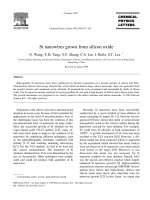
Fig. 2a shows the SEM image of the Cu clusters deposited on the Si
wafer. The diameter of most Cu clusters is about 5 nm (Fig. 2b), almost
the same as the expected 4 nm. The size distribution is relatively uni-
form due to the mass filter in the ND 60. To investigate the diameter
variation of the catalyst during heating, the Si wafer covered with Cu
clusters has been heated on 500 °C without any gas feeding. Fig. 2c
depicts the diameter distribution of the after-heated Cu catalyst. The Cu
clusters have aggregated into the larger nanoparticles and the diameter
distribution becomes wider. After being heated in the high temperature
tube furnace with SiH
4
feeding, the surface of the Si wafer changed to
light yellow. SEM image (Fig. 2d) of the after-grown Si wafer demon-
strates that there are many thin and straight nanowires covering the
surface of the Si wafer. The nanowires prolong several micrometers
randomly. In the high magnification image (Fig. 2e), a small spot can
be observed on tip of the straight nanowire and the diameter of the tip is
as the same as the nanowires.
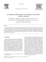
The Si nanowires have been scraped from the Si wafer and moved
to Cu grid for TEM characterization. Fig. 3a displays the low mag-
nification TEM image of the Si nanowires. Some silicon particles are
mixed with the Si nanowires. A straight nanowire 30 nm wide, a typical
diameter for the thin Si nanowires is shown in Fig. 3b. There is a 4 nm
thick amorphous layer covering the nanowire. The high resolution
TEM image (down image inserted in Fig. 3b) reveals that the straight
Si nanowire is well crystalline. Diffractogram patterns, a fast Fourier
transformation (FFT) from the high resolution image, indicate that the
growth direction of the Si nanowires is along b111N (up image inserted
in Fig. 3b). The lattice distance along the growth direction of the
nanowires is about 3.14 Å, which well agrees with the distance
between Si {111} facets. However, the contrast variation on the
nanowires in the low magnification TEM image (Fig. 3b) indicates that
there should be some defects in the Si nanowires. As disclosed in
Fig. 3c, the {111} stack faults and micro-twin boundaries are the
dominated defects in the Si nanowires.
There is a polyhedron dark tip with the flat facets on the straight Si
nanowire. Fig. 3d shows the clear lattices contrast of both Si nanowire
and the dark tip. The size of the tip is as large as the diameter of the Si
nanowires. It is different with the preview reports about the Au
catalyzing Si nanowires, in which the tips are ball-like Au particles [1–
3]. Fig. 3e is the diffractogram patterns of the interface between the tip
and the nanowire. Two groups of patterns can be distinguished: one
should be indexed as the diffraction patterns of Si (0 1
¯
1
¯
)* reversal
plane, another could be ascribed to orthorhombic η″-Cu
3
Si (1
¯
, 19, 0)*
reversal plane [18]. The diffractogram spots are indexed in Fig. 3e with
solid and dashed lines. The {111} facet of Si nanowires is almost
parallel to the {003} facet of the η″-Cu
3
Si. The diffractogram patterns
of the alloy tip are also displayed in Fig. 3f and the sharp spots prove
that the tip is the single crystal η″-Cu
3
Si alloy. This result confirms that
the copper-rich η″-CuSi alloy should be formed when the alloy liquid is
cooled down to the room temperature (Fig. 1).
An interesting result that should be emphasized is that the growth
temperature of the Si nanowires is 500 °C, much lower than the eutectic
temperature 802 °C. It means that the VLS mechanism should not
occur during the growth. The formation of Si nanowires may be
ascribed to the vapor–solid (VS) growth mechanism. Under the frame-
work of VS mechanism, the decomposed Si from SiH
4
deposits on the
surface of Cu nanoparticles and forms solid η′-CuSi alloy (between
467 °C and 558 °C). The Si diffuses in the solid–solution alloy and will
Fig. 1. Cu–Si phase diagram [17].
178 Y. Yao, S. Fan / Materials Letters 61 (2007) 177–181
separate from the solid alloy to form the Si nanowires when the
concentration is supersaturated. The diameter of the Si nanowires is
similar to the size of the CuSi alloy nanoparticles. So the tip of the Si
nanowires is polyhedron, not the ball-like tip.
4. Conclusion
The Si nanowires could be grown with Cu catalyst. The
diameter of the Cu nanoparticles could affect the size and the
quantity of the nanowires. The growth temperature is 500°C and
the growth direction of the Si nanowires is b111N. TEM images
indicate the well crystalline of the thin and straight Si nanowires
with η″-Cu
3
Si alloy tips. VS growth mechanism should be
responsible for the formation of Si nanowires. The cheap Cu
catalyst and the low growth temperature are favorable to the
mass synthesis of the Si nanowires.
Acknowledgements
Financial support from the National Natural Science Founda-
tion of China (NNSFC 10334060) and National Basic Research
Program of China (973 Program 2005CB623606) is gratefully
acknowledged. The authors also thank Mr. Liguo Xu for his
helpful assistant work.
Fig. 2. The SEM images of a) the Cu nanoparticles on the surface of Si wafer (scale bar is 1 μm). b) The diameter distribution of the Cu nanoparticles. c) The diameter
distribution of the after-heated Cu nanoparticles. d) The Si nanowires grown on the Si wafer (scale bar is 5 μm). e) The large magnification SEM images of a Si
nanowire (scale bar is 1 μm).
179Y. Yao, S. Fan / Materials Letters 61 (2007) 177–181
Fig. 3. a) The low magnification TEM image of the Si nanowires. b) The TEM image of a straight Si nanowire. (The down inserted image is the high resolution image
of the nanowires and the up inserted image is the corresponding diffractogram patterns.) c) The {111} stack faults and micro-twins in the straight Si nanowire. d) High
resolution image of the tip. e) The diffractogram patterns of the interface between the tip and the nanowire. (The solid and dashed lines indicate the patterns from Si and
η″-Cu
3
Si alloy, respectively.) f) The diffractogram patterns of the dark tip.
180 Y. Yao, S. Fan / Materials Letters 61 (2007) 177–181
References
[1] Y. Cui, X. Duan, J. Hu, C.M. Lieber, J. Phys. Chem., B 104 (2000) 5213.
[2] Y. Cui, C.M. Lieber, Science 291 (2001) 851.
[3] Y. Cui, Q. Wei, H. Park, C.M. Lieber, Science 293 (2001) 1289.
[4] X.T. Zhou, J.Q. Hu, C.P. Li, D.D.D. Ma, C.S. Lee, S.T. Lee, Chem. Phys.
Lett. 369 (2003) 220.
[5] S.Q. Feng, D.P. Yu, H.Z. Zhang, Z.G. Bai, Y. Ding, J. Cryst. Growth 209
(2000) 512.
[6] J. Qi, A.M. Belcher, J.M. White, Appl. Phys. Lett. 82 (2003) 2616.
[7] D.D.D. Ma, S.T. Lee, J. Shinar, Appl. Phys. Lett. 87 (2005) 033107.
[8] R.S. Wagner, W.C. Ellis, Appl. Phys. Lett. 4 (1961) 89.
[9] Y. Cui, L.J. Lauhon, M.S. Gudiksen, J. Wang, C.M. Lieber, Appl. Phys.
Lett. 78 (2001) 2214.
[10] Y. Yao, F.H. Li, S.T. Lee, Chem. Phys. Lett. 406 (2005) 381.
[11] S. Ge, K. Jiang, X. Lu, Y. Chen, R. Wang, S. Fang, Adv. Mater. 17 (2005)
56.
[12] A.I. Hochbaum, R. Fan, R. He, P. Yang, Nano Lett. 5 (2005) 457.
[13] D.P. Yu, Y.J. Xing, Q.L. Hang, et al., Phys. E 9 (2001) 305.
[14] M. Morales, C.M. Lieber, Science 279 (1998) 208.
[15] S. Jin, Q. Li, C.S. Lee, Phys. Status Solidi, A Appl. Res. 188 (2001) R1.
[16] D.A. Hodges, H.G. Jackson, R.A. Saleh. Analysis and Design of Digital
Int egrated Circuits in Deep Submicron Technolog y, Third Edition
(McGraw-Hill Companies, Inc.).
[17] T.B. Massalski, Binary Alloy Phase Diagram, Second editionASM
International, 1990.
[18] J.K. Solberg, Acta Crystallogr., A 34 (1978) 684.
181Y. Yao, S. Fan / Materials Letters 61 (2007) 177–181