Hướng dẫn sử dụng Electronic and electrical
Bạn đang xem bản rút gọn của tài liệu. Xem và tải ngay bản đầy đủ của tài liệu tại đây (3.59 MB, 257 trang )
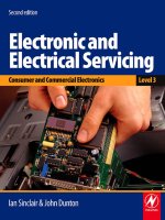
Electronic and Electrical
Servicing
Consumer and commercial electronics
Second Edition – Level 3
Ian Sinclair
and
John Dunton
AMSTERDAM • BOSTON • HEIDELBERG • LONDON • NEW YORK • OXFORD
PARIS • SAN DIEGO • SAN FRANCISCO • SINGAPORE • SYDNEY • TOKYO
Newnes is an imprint of Elsevier
Newnes is an imprint of Elsevier Ltd
Linacre House, Jordan Hill, Oxford OX2 8DP
30 Corporate Road, Burlington, MA 01803
First published 2002
Reprinted 2003
Second edition 2007
Copyright © 2007, Ian Sinclair and John Dunton. Published by Elsevier Limited.
All rights reserved
The right of Ian Sinclair and John Dunton to be identifi ed as the authors of this
work has been asserted in accordance with the Copyright, Designs and Patents
Act 1988
No part of this publication may be reproduced, stored in a retrieval system or
transmitted in any form or by any means electronic, mechanical, photocopying,
recording or otherwise without the prior written permission of the publisher
Permission may be sought directly from Elsevier’s Science & Technology Rights
Department in Oxford, UK: phone (ϩ44) (0) 1865 843830; fax (ϩ44) (0) 1865
853333; email: Alternatively you can submit your
request online by visiting the Elsevier web site at />permissions, and selecting Obtaining permission to use Elsevier material
Notice
No responsibility is assumed by the publisher for any injury and/or damage to
persons or property as a matter of products liability, negligence or otherwise, or
from any use or operation of any methods, products, instructions or ideas contained
in the material herein. Because of rapid advances in the medical sciences, in
particular, independent verifi cation of diagnoses and drug dosages should be made
British Library Cataloguing in Publication Data
A catalogue record for this book is available from the British Library
Library of Congress Cataloguing in Publication Data
A catalogue record for this book is available from the Library of Congress
ISBN: 978-0-7506-8732-4
For information on all Newnes publications
visit our web site at www.books.elsevier.com
Typeset by Charon Tec Ltd (A Macmillan Company), Chennai, India
www.charontec.com
Contents
Preface to the second edition – level 3 iv
Acknowledgements iv
Unit 1 1
26 Sine wave driven circuits 2
27 Transformers and power transfer 20
28 Semiconductors, active devices and transducers 31
Unit 2 56
29 Meters and data 57
30 The analogue oscilloscope 72
31 Test and measurement 85
32 Rework, repair, reliability, safety and European Union directives 103
Unit 3 124
33 Direct current power supplies 125
34 Analogue amplifi ers 144
35 Oscillators and waveform generators 172
Unit 4 184
36 Logic families and terminology 185
37 Sequential logic 198
38 Digital communications 215
39 Test equipment and fault-fi nding 230
Answers to multiple-choice questions 245
Index 246
Preface to the second
edition – Level 3
This new edition of Electronic and Electrical Servicing refl ects the rapid
changes that are taking place within the electronics industry. In particular, we
have to recognise that much of the equipment that requires servicing will be
of older design and construction; by contrast, some modern equipment may
require to be replaced under guarantee rather than be serviced. We also need
to bear in mind that servicing some older equipment may be totally uneco-
nomical, because it will cost more than replacement. With all this in mind, this
new edition still provides information on older techniques, but also indicates
how modern digital systems work and to what extent they can be serviced.
This volume is intended to provide a complete and rigorous course of
instruction for the core units of Level 3 of the City & Guilds Progression
Award in Electrical and Electronics Servicing – Consumer/Commercial
Electronics (C&G 6958). It follows on from the Level 2 book (as do the
chapter numbers), which covers all the core units and two of the option
units at this level (ISBN 978-0-7506-6988-7).
Acknowledgements
The development of this series of books has been greatly helped by the City &
Guilds of London Institute (CGLI), the Electronics Examination Board
(EEB) and the Engineering & Marine Training Authority (EMTA). We are
also grateful to the many manufacturers of electronics equipment who have
provided information on their websites.
Ian Sinclair
John Dunton
Unit 1
1. Demonstrate an understanding of reactance, resonance, transform-
ers and transfer and the practical application of these components
and circuits
2. Demonstrate an understanding of semi-conductor devices, displays
and transducers and the practical applications of these components.
Outcomes
26
Sine wave driven
circuits
Capacitors and inductors in direct current (d.c.) circuits cause transient cur-
rent effects only when the applied voltage changes. In an alternating cur-
rent (a.c.) circuit this is a continuous process. Capacitors in such a circuit
are therefore continually charging and discharging, and inductors are con-
tinually generating a changing back-electromotive force (emf). Circuits
containing resistors, capacitors and inductors are described as complex
circuits and an alternating voltage will exist across each component pro-
portional to the magnitude of current fl owing through it so that a form of
Ohm’s law still applies.
In the explanation that follows, the symbols VЈ and IЈ are used to mean
peak a.c. values (Figure 26.1) of alternating signals. Root mean square
(r.m.s.) values are represented by V
rms
and I
rms
; that is,
II
rms
ϭЈ/2
. The
symbols v and i represent instantaneous values of a.c. signals and V and I will
have their usual meaning of d.c. values. So, we may write v ϭ VЈ sin (2πft).
V',I'
0
T
t
Figure 26.1 The peak value and period of a sine wave of voltage or current
For a resistor in an a.c. circuit, VЈ ϭ R ϫ IЈ and the value of resistance found
from the variant form of this equation,
R
V
I
ϭ
Ј
Ј
, is the same as the d.c. value,
V
/I. In a capacitor or an inductor, the ratio VЈ/IЈ is called reactance, with
the symbol X. Because this is a ratio of volts to amperes, the same units Ω
(ohms) are used as used to express d.c. resistance, but it must be remem-
bered this is a frequency-dependent reactance and not a resistance.
A capacitor may, for example, have a reactance of only 1 KΩ at a given
frequency, but a d.c. resistance that is unmeasurably high. An inductor may
Sine wave driven circuits 3
have a d.c. resistance of 10 ohms, but a reactance of 5 KΩ or more. The react-
ance of a capacitor or an inductor is not a constant quantity, but depends
on the frequency of the applied signal. A capacitor, for example, has a very
high reactance to low-frequency signals and a very low reactance to high-
frequency signals, as indicated in Figure 26.2.
10
100 1k 10k 100k
1
10
100
1k
10k
100k
1M
470pF
1nF
2n2F
4n7F
10nF
22nF
47nF
100nF
220nF
470nF
1μF
2μ2F
4μ7F
10μF
100μF
Reactance in Ohms
Frequency in Hz
Figure 26.2 Chart of capacitive reactance at audio frequencies
The reactance of a capacitor VЈ/IЈ can be calculated from the equation:
X
fC
C
ϭ
1
2π
ohms
where f is the frequenc
y of the signal in Hz and C is the capacitance in
farads. Figures 26.2 and 26.3 show the values of capacitive reactance for
a range of different capacitors calculated for a range of frequencies. These
charts are intended as a guide so that you can quickly estimate a reactance
value without the need to make the calculations.
The reactance of an inductor varies in the opposite way, being low for
low-frequency signals and high for high-frequency signals. Its value can be
calculated from the equation:
X
L
ϭ 2πfL ohms
where f is the frequency in Hz and L is the inductance in henries. Figures
26.4 and 26.5 show the values of inductive reactance which are found at
various frequencies.
4 Electronic and electrical servicing
100k
1M 10M 100M 1G
1
10
100
1k
10k
100k
1M
1pF
4p7F
2p2F
10pF
22pF
47pF
100pF
220pF
470pF
1nF
10nF
100nF
Reactance in Ohms
Frequency in Hz
Figure 26.3 Chart of capacitive reactance at radio frequencies
10
100 1k 10k 100k
1
100
10
1k
10k
100k
1M
10M
10H
5H
2H
1H
500mH
200mH
100mH
50mH
20mH
Reactance in Ohms
Frequency in Hz
Figure 26.4 Inductive reactance at audio frequencies
Sine wave driven circuits 5
Note: inductors are now less common in circuits other than power sup-
ply and radio (transmission and reception) applications. The increasing
use of inte
grated circuits (ICs) and digital circuitry has made the use
of inductors unnecessary in a very wide range of modern applications.
10k
100k 1M 10M 100M
10mH
5mH
2mH
1mH
500μH
200μH
100μH
50μH
20μH
Reactance in Ohms
Frequency in Hz
1
10
100
1k
10k
100k
1M
10M
Figure 26.5 Inductive reactance at radio frequencies
Connect the circuit shown in Figure 26.6. If meters of different ranges
have to be used, changes in the values of capacitor and inductor will
also be necessary. The signal generator must be capable of supplying
enough current to defl ect the current meter which is being used.
Figure 26.6 Circuit for practical
Practical 26.1
(Continued)
6 Electronic and electrical servicing
There is another important difference between a resistance and a capacitive
or inductive reactance and this can be demonstrated as follows. With the aid of
a double-beam oscilloscope, the a.c. waveform of the current fl owing through
a resistor and the voltage developed across it can be displayed together (Figure
26.7). This shows that the two waves coincide, with the peak current coinciding
with the peak voltage, etc. If this experiment is repeated with a capacitor or an
inductor in place of the resistor, you will see from the fi gure that the waves of
current and voltage do not coincide, but are a quarter-cycle (90º) out of step.
Connect a 4.7 μF capacitor between the terminals, and set the sig-
nal generator to a frequency of 100 Hz. Adjust the output so that read-
ings of a.c. voltage and current can be made. Find the value of VЈ/IЈ’
at 100 Hz.
Repeat the measurements at 500 Hz and at 1000 Hz. Tabulate val-
ues of X
C
ϭ VЈ/IЈ and of frequency f.
Now remove the capacitor and substitute a 0.5 H inductor. Find
the reactance at 100 Hz and 1000 Hz as before, and tabulate values of
X
L
ϭ VЈ/IЈ and of frequency f.
Next, either remove the core from the inductor or increase the size
of the gap in the core (if this is possible), and repeat the measure-
ments. How has the reactance value been affected by the change?
Practical 26.1 (Continued)
Current
Voltage across resistor
Voltage across capacitor
Voltage across inductor
Capacitor: I leads V by 90Њ
Inductor: V leads I by 90Њ
Figure 26.7 Phase shift caused by a reactance
Comparing the positions of the peaks of voltage and of current, you can
see that:
• For a capacitor, the current wave leads (or precedes) the voltage wave
by a quarter-cycle.
• For an inductor, the voltage wave leads the current wave also by a
quarter-cycle.
Sine wave driven circuits 7
An alternative way of expressing this is that, for a capacitor, the voltage
w
ave lags (or arrives after) the current wave by a quarter-cycle, and for an
inductor, the current wave lags the voltage wave by a quarter-cycle.
The amount by which the waves are out of step is usually defi ned by the
phase angle. The current and voltage waves are 90º out of phase in a reac-
tive component such as a capacitor or an inductor.
A useful way to remember the phase relationship between the cur-
rent and voltage is the word C-I-V-I-L, meaning C–I leads V; V leads
I–L. The letters C and L are used to denote capacitance and induct-
ance, respectively.
If we take a few measurements on circuits containing reactive compo-
nents we can see that the normal circuit laws used for d.c. circuits cannot
be applied directly to a.c. circuits.
Consider, for example, a series circuit containing a 10 μF capacitor C, a 2 H
inductor L and a 470 ohm resistor R, as in Figure 26.8(a). With 10 V a.c. volt-
age, VЈ at 50 Hz applied to the circuit, the a.c. voltages across each component
can be measured and added together: VЈ
C
ϩ VЈ
L
ϩ VЈ
R
. You will fi nd that these
measured voltages do not add up to the voltage VЈ across the whole circuit.
V
Ј
R
V
Ј
C
V
Ј
470Ω 10μF
Signal
generator
V
Ј
V
Ј
R
V
Ј
C
V
Ј
L
470Ω 10μF
2H
Signal
generator
(a)
(b)
Figure 26.8 Series circuits: (a) RLC, and (b) RC circuit for practical
example
Connect the circuit shown in Figure 26.8(b). Use either a high-
resistance a.c. voltmeter or an oscilloscope to measure the voltage
VЈ
R
across the resistor and the voltage VЈ
C
across the capacitor. Now
measure the total voltage VЈand compare it with VЈ
R
ϩ VЈ
C
.
Practical 26.2
8 Electronic and electrical servicing
The reason why the component voltages in a complex circuit do not add
up to the circuit voltage when a.c. fl ows through it is due to the phase angle
between voltage and current in the reactive component(s). At the peak of
the current wave, for example, the voltage wave across the resistor will also
be at its peak, but the voltage wave across any reactive component will be
at its zero value. Measurements of voltage cannot, however, indicate phase
angle. They can only give the r.m.s. or peak values for each component, and
the fact that these values do not occur at the same time cannot be allowed
for by meter measurement. The result is that straight addition of the meas-
ured value will inevitably give a wrong result for total voltage, because of
the time difference.
Phasor diagrams (often also called vector diagrams) are one method of
performing the addition so that phase angle is allowed for. In a phasor dia-
gram, the voltage across a resistor in an a.c. series circuit is represented
by the length of a horizontal line drawn to scale. Voltages across reactive
components are represented by the lengths of vertical lines, also drawn to
the same scale. If all the lines are drawn from a single point, as in Figure
26.9(a), the resulting diagram is a phasor diagram that represents both the
phase and the magnitude of the voltage wave across each component.
IV
R
V
L
V
C
V
R
V
C
I
V
L
V
L
ϪV
C
∅
V
R
V
L
ϪV
C
V
R
2
ϩ(V
L
ϪV
C
)
2
(a) (b) (c)
Figure 26.9 Phasor diagrams for complex series circuits: (a) relationship
between V and I for a series RLC circuit, (b) combining V
L
and V
C
, and (c)
fi nding the total voltage across the circuit
To represent the opposite effects that capacitors and inductors have on
the phase, the vertical line representing voltage across an inductor is drawn
vertically upwards, and the line representing voltage on a capacitor is
drawn vertically downwards. By convention, an inductive reactance and the
voltage across it are considered to be positive. A capacitive reactance and
its voltage are considered to be negative.
The phasor diagram can now be used to fi nd the total voltage across the
whole circuit. First, the difference between total upward (inductive) and total
downward (capacitive) voltage is found, and a line is drawn to represent
the size and direction of this difference. For example, if the inductive volt-
age is 10 V and the capacitive voltage 7 V, the difference is 3 V drawn to
scale in the direction of inductive reactance. If the inductive voltage were
Sine wave driven circuits 9
10 V and the capacitive voltage 12 V, the difference would be 2 V drawn to
scale do
wnwards in the capacitive direction.
The net reactive voltage so drawn is then combined with the voltage across
the resistor in the following way. Starting from the point marking the end of
the line representing the voltage across the resistor, draw a vertical line, as in
Figure 26.9(b), to represent the net reactive voltage in the correct direction,
up or down. Then connect the end of this vertical line to the starting point
(Figure 26.9c). The length of this sloping line will give the voltage across
the whole circuit, and its angle to the horizontal will give the phase angle
between voltage and current in the whole circuit.
The total voltage can be found by Pythagoras’ rule, since the phasor
relationship is that of a right-angle triangle, so the total voltage is
′′
+
′′
VVVV
TRLC
ϭ Ϫ
222
()
.
A comple
x circuit which contains both resistance and reactance possesses
another characteristic which is of great importance. This characteristic is
known as impedance, symbol Z. Impedance is measured in ohms, and is
equal to VЈ/IЈ for the whole circuit. Its value varies as the frequency of the
signal varies.
When impedance is present, the phase angle between current and voltage
is less than 90º in either direction. This phase angle can be found most eas-
ily by using the phasor diagram in a slightly different way, to form what is
known as the impedance triangle.
In a phasor diagram constructed this way (Figure 26.10), separate lines
are drawn to represent the resistance R, the reactance X and the impedance
Z. In a series circuit, the length of the horizontal line represents the total
value of resistance in the circuit, and the vertical line its net value of react-
ance upwards as before, for predominantly inductive reactance (a), and
downwards for predominantly capacitive reactance (b).
(a) (b)
R
X
Z
∅
R
X
Z
∅
Figure 26.10 Impedance triangle: (a) predominantly inductive, and (b)
predominantly capacitive
With the values of R and X known and the angle between them a right
angle, the Z line can be drawn in, representing the impedance value of the
whole circuit. The angle of this line to the horizontal is the phase angle
between current and voltage in the circuit.
Another way of working out the relationships between R, X and Z in a
complex circuit is to express them by two algebraic formulae:
ZXX R XXR
LC LC
ϭϪϩ ϭϪ() )/
22
and tan (ϕ
10 Electronic and electrical servicing
where Z ϭ total impedance, X
L
ϭ inductive reactance, X
C
ϭ capacitive react-
ance, ϕ ϭ phase angle, and R ϭ the resistance of the circuit as a whole.
A pocket calculator covering a reasonably full range of mathematical func-
tions can now be used to work out the values of circuit impedance and phase
angle.
Filters are circuits that are designed to separate out a range of frequencies
of interest that are present in any waveband. Because these are frequency
dependent, the circuits must contain at least one reactive component.
In the low-pass fi lter (LPF) shown in Figure 26.11(a), the inductor has
a low series reactance at low frequencies so that these pass easily to the
output and are developed as the output signal V
out
. In Figure 26.11(b), the
capacitor has a very high reactance at low frequencies and acts as the load
to develop the output signal V
out
. At high frequencies the low reactance of
C effectively short-circuits the output signal.
Filters
V
in
L
(a)
R
V
out
V
in
R
(b)
C
V
out
V
out
/V
in
Ϫ3dB
Ϫ20
0
Ϫ40
Ϫ60
Ϫ80
f
bp
(c)
Figure 26.11 Low-pass fi lters: (a) LR, (b) CR, and (c) typical response
Figure 26.11(c) shows the amplitude of the output signal plotted against
frequency for both the LR and CR circuits and this also represents the vari-
ation of circuit impedance with frequency. The Ϫ3 dB or half power point of
the frequency response represents the break point where the circuit react-
ance is equal to its resistance value. This point is defi ned by the formula
f ϭ 1/(2πCR) Hz or f ϭ 1/(2π(L /R)) Hz
and is therefore dependent on the circuit time constant.
For the high-pass fi lters (HPFs) shown in Figure 26.12(a, b), the resistors
and reactors are interchanged to produce the opposite effect. Figure 26.12(c)
Sine wave driven circuits 11
again shows the attenuation effects and the variation of circuit impedance,
with the break point calculated as before.
V
in
R
(a)
L
V
out
V
in
C
(b)
R
V
out
V
out
/V
in
Ϫ3dB
Ϫ20
0
Ϫ40
Ϫ60
Ϫ80
f
bp
(c)
Figure 26.12 High-pass fi lters: (a) LR, (b) CR, and (c) typical response
For both of the fi rst order LPF and HPF circuits with a single pair of
components shown above, the straight part of the attenuation slope falls
away at 6 dB per octave (a doubling or halving of frequency).
For an LPF and an HPF as shown in Figures 26.11 and 26.12, set up
a circuit so that the signal current through the fi lter can be plotted
against frequency. How do these results compare with the shape of
the attenuation characteristics?
Practical 26.3
A circuit that selects a band of frequencies is described as a band-pass
fi lter (BPF) and one such circuit can be constructed as shown in Figure 26.13.
This is effectively a cascade of an LPF and an HPF and its attenuation char-
acteristic is shown in Figure 26.13(b). The attenuation slope at both ends is
still Ϫ6 dB per octave. The two Ϫ3 dB break points of the individual low-
and high-pass sections are calculated from the equations
f
1f
ϭ 1/(2πC
1
R
1
) Hz and f
hf
ϭ 1/(2πC
2
R
2
) Hz
12 Electronic and electrical servicing
and if the stages did not load each other the bandwidth of the circuit would
simply be the difference between these two frequencies. This is rarely the case
for practical values and in effect the high- and low-pass corners are pulled
towards each other by the loading effects. This type of fi lter can suffer from
quite large in-band insertion losses, particularly if the RC sections are chosen
to minimize load effects; it is often useful to put a buffer amplifi er in between
the stages to restore the losses and isolate the stages from each other.
V
in
V
out
R
RC
C
(a)
V
out
/ V
in
0
Ϫ20
Ϫ3dB
Ϫ40
Ϫ60
Ϫ80
Insertion loss
Frequencyf
ifbp
f
hfbp
(b)
Figure 26.13 (a) Band-pass fi lter circuit, and (b) typical response
A band-stop fi lter (BSF), which has the opposite characteristic of the BPF,
cannot be conveniently constructed using the cascading principle shown above.
For these circuits it is more usual to use second order fi lters as shown in
Figure 26.14(a). This particular circuit is referred to as a twin or parallel
T device, where the ratios of the component values are chosen as:
C
2
ϭ 2C
1
and R
1
ϭ R
2
/2
so that the maximum attenuation occurs at f ϭ 1/(2πR
1
C
1
) Hz.
The values of capacitive reactance, X
C
, and inductive reactance, X
L,
are fre-
quency dependent but have opposite slopes. At low frequencies, X
C
is large
and X
L
small, a situation that becomes reversed at high frequencies. There
must therefore be some frequency at which X
C
ϭ X
L
. This frequency is
called the resonant frequency, or the frequency of resonance, of the LCR
circuit in question. Its symbol is f
r
.
A phasor diagram drawn for a series LCR circuit at its resonant frequency
will clearly have a zero vertical component of reactance (Figure 26.15). The
Resonance
Sine wave driven circuits 13
R
1
C
1
R
1
C
1
C
2
R
2
(a)
V
in
V
out
C
2
ϭ 2C
1
R
2
ϭ 2R
1
f
c
0dB
V
out
/V
in
(b)
Figure 26.14 Band-stop fi lter (twin-T): (a) circuit, and (b) typical response
XΩ
X
C
X
L
(a) (b)
f Hz
X
L
X
C
R
Figure 26.15 Resonance in a series LCR circuit
14 Electronic and electrical servicing
impedance of the circuit will therefore be simply equal to its resistance. The
same conclusion can be reached by working out the impedance formula:
ZXX R
LC
ϭϪϩ()
22
At its resonant frequency, therefore, an LCR circuit behaves as if it contained
only resistance, and has zero phase angle between current and voltage.
Practical 26.4
Connect the circuit shown in Figure 26.16 with component values as
follows: R ϭ 1 K, C ϭ 0.1 μF and L ϭ 80 mH. The resonant frequency
of the circuit is about 1.8 kHz. Set the signal generator to 100 Hz,
and connect the oscilloscope so as to measure the voltage across the
resistor R. This voltage will be proportional to the amount of current
fl owing through the circuit, because V ϭ R ϫ I. Now increase the fre-
quency, watching the oscilloscope. The resonant frequency is the fre-
quency at which current fl ow (and therefore the voltage across R) is
a maximum. Note this frequency, and the value of the amplitude of
the voltage across R at the resonant frequency. Measure the voltages
across L and across C by connecting the oscilloscope across each in
turn. Note the value of these voltages. Finally, use the oscilloscope to
measure the voltage across the whole circuit. Construct a phasor dia-
gram for the voltages across R, C and L and confi rm that this produces
an answer for the total voltage. (Remember that the oscilloscope itself
will disturb the circuit to some extent, and that the resistance of the
inductor has not been taken into account in your calculation.)
Signal
generator
L
80mH
C
0.1μF
R
1kΩ
To
oscilloscope
Figure 26.16 Circuit for practical exercise, series resonance
Sine wave driven circuits 15
In a series-resonant circuit, the current fl
ow at resonance in the circuit will
be large if the voltage across the whole circuit remains constant. Therefore,
a large voltage will exist across each of the reactive components. In gen-
eral, the voltage across both the capacitor and the inductor will be greater
than the voltage across the whole circuit at the resonant frequency.
The ratio VЈ
X
/VЈ
Z
, where VЈ
X
is the voltage across a reactor and VЈ
Z
is the
voltage across the whole circuit, is called the circuit magnifi cation factor,
symbol Q, which can be very large at the frequency of resonance.
The frequency of resonance for a series circuit can be calculated by using
the formula:
f
LC
ϭ
1
2π
where L is the inductance (henries), C the capacitance (f
arads), and f is the
frequency (hertz).
Example: What is the resonant frequency of a circuit containing a
200 mH inductor and a 0.05 mF capacitor?
Solution: Substitute the data in the equation, taking care to reduce both
L and C to henries and farads, respectively. Use L ϭ 200 ϫ 10
–3
ϭ 0.2 H and
C ϭ 0.05 ϫ 10
–6
ϭ 5 ϫ 10
–
8 F. Take 2π as being approximately 6.3. Then:
f
r
ϭ
ϫϫ
ϭ
Ϫ
1
63 02 5
1587
(. . )10
Hz
8
Find (in MHz, to two decimal places) the resonant frequency of the series
combination of a 220 pF capacitor and a 15 μH inductor.
A circuit consisting of inductance, capacitance and resistance in parallel
will resonate at a frequency given approximately by the same equation that
was used for series resonance. However, in a practical circuit, the resistive
component is more likely to be the inherent resistance of the inductor; in
which case the circuit now consists of C in parallel with L plus a series
resistance R that represents this component’s losses. The frequency of reson-
ance for this circuit is given by:
f
LC
R
L
ϭϪ
1
2
1
2
2
π
If R is small, as is usually the case, the R
2
/L
2
component can be neglected
and the resonance frequency formula reverts to that for series resonance. The
lossy term R
2
/L
2
is related to the Q factor (or quality factor, Q ϭ 2πfL/R)
of the inductor, so that if Q is higher than about 50 the simplifi ed formula
is accurate enough for most applications.
At the frequency of resonance, a parallel resonant circuit behaves like a
high value of resistance, L/CR, which is called the dynamic resistance or
16 Electronic and electrical servicing
impedance. Again, at resonance, the phase angle between voltage and cur-
rent is zero.
Practical 26.5
Connect the parallel resonant circuit of Figure 26.17 to the signal
generator. Find the frequency of resonance, which for the component
values shown will be about 2250 Hz, and note that at this resonant
frequency, the voltage across the resonant circuit is a maximum. Now
connect another 0.047 μF capacitor in parallel with C, and note the
new frequency of resonance. Remove the additional capacitor, and
plot a graph of the voltage across the resonant circuit against fre-
quency, for a range of frequencies centred about the resonant fre-
quency. Observe the shape of the resulting curve, which is called the
resonance or response curve. Now add a 10 K resistor in parallel with
the resonant circuit, and plot another resonance curve, using the same
frequency values. What change is there in the shape of the curve?
Repeat the experiment using a 1 K resistor in place of the 10 K one,
and plot all three graphs on the same scale.
Signal
generator
L
100mH
R
47kΩ
C
47nF
To
oscilloscope
Figure 26.17 Circuit for practical exercise, parallel resonance
The results of these experiments will show that the addition of either capaci-
tance or inductance to a parallel resonant circuit causes the frequency of
resonance to become lower. The addition of resistance in parallel has little
Bandwidth
Sine wave driven circuits 17
effect on the frequency of resonance, but a considerable effect on the shape
of the resonance curv
e. The effect of adding a small value of resistance is
to lower the peak of the resonance curve, as might be expected because the
sum of two resistors in parallel is a net resistance smaller than either. In
addition, however, the width of the curve is increased.
A resistor used in this way is called a damping resistor or de-Quing
resistor, since it reduces the Q of the circuit. Its effect is to make the reson-
ant circuit respond to a wider range of frequencies, but at a lower amplitude.
A damping resistor therefore increases the bandwidth of a resonant cir-
cuit, making the circuit less selective of frequency. When a parallel reson-
ant circuit is used as the load of an amplifi er, the tuned frequency is the
resonant frequency of the parallel circuit, and the amount of damping resist-
ance used will determine the bandwidth of the amplifi er (Figure 26.18).
With damping
resistor
No damping
resistor
Low value
damping resistor
1k
2m
4m
10m
20m
40m
100m
200m
400m
2k 3k 4k 5k 6k 7k 8k 9k 10
k
V
out
/V
in
Frequency/Hertz
Figure 26.18 Effect of adding a damping resistor to a parallel resonant circuit
Using LCR circuits allows us to construct band-pass and band-stop fi lters
which are more effi cient than those described above. The simple LC paral-
lel or series circuits can have resistors added to dampen the resonance so
that the resonant effect is reduced but spread over a wider range of frequen-
cies, providing a simple band-pass or band-stop action according to where
the resonant circuit is placed.
For many purposes, however, these circuits do not provide a sharp enough
distinction between the pass and the stop bands and much more elaborate
fi lter circuits have to be devised. Band-pass and band-stop characteristics
18 Electronic and electrical servicing
are often plotted on a linear scale of frequency so that the bandwidth is
easier to read from the graph, but the attenuation is always plotted in terms
of decibels.
Calculations on such fi lters are very diffi cult. Standard fi lter tables are
published which reduce the design effort to scaling for the impedance and
frequency, and computer programs such as SPICE can be used to graph the
response for any combination of components. Figure 26.19(a) shows a BPF,
using a combination of series and parallel circuit to determine the band-
pass mid-frequency. The graph in Figure 26.19(b) shows the response of
this circuit for the component values shown. It should be noted that there is
signifi cant insertion loss and ripple in the pass band. The ripple and losses
can be minimized by careful design taking account of factors like the d.c.
resistance of the inductors and tolerance of all the components, but this is
beyond the scope of this book.
L
1
24mH
C
1
27nF
C
2
120nF
L
2
5mH
75Ω75Ω
L
3
24mH
C
3
27nF
(a)
V
out
/V
in
(dB)
Ϫ20
0
Ϫ40
Ϫ60
Ϫ80
Ϫ100
Ϫ120
Ϫ140
100 200 500 1k 2k 5k 10k 20k 50k 100k 200k 500k 1M
Frequency/Hertz
(b)
Figure 26.19 (a) Circuit, and (b) computed response curve for a band-pass fi lter
Sine wave driven circuits 19
26.1 In a series circuit made from a resistor
and a capacitor the voltage across the
resistor is 100 V and the total circuit
voltage is 141.4 V. What is the voltage
across the capacitor?
(a) 50 V
(b) 75 V
(c) 100 V
(d) 150 V.
26.2 In the circuit in question 26.1 the current
is 1 A. What is the value of the resistor?
(a) 1 Ω
(b) 10 Ω
(c) 100 Ω
(d) 1000 Ω.
26.3 In the circuit in question 26.1 the current
is 1 A. What is the value of the capacitor
if the source frequency is 50 Hz?
(a) 16 μF
(b) 32 μF
(c) 64 μF
(d) 100 μF.
26.4 An RC low-pass fi lter uses a 47 kΩ
resistor and a 33 nF capacitor. What is the
frequency at which the output voltage is
Ϫ3 dB relative to the input?
(a) 97.4 kHz
(b) 645 kHz
(c) 103 kHz
(d) 155.1 kHz.
26.5 A parallel circuit consisting of a variable
capacitor and a 160 μH coil is used in a
radio receiver to select a station whose
frequency is 1215 kHz. What value will
the variable capacitor have when the
station is correctly tuned?
(a) 75.9 pF
(b) 107.2 pF
(c) 151.8 pF
(d) 300 pF.
Multiple-choice revision questions
27
Transformers and
power transfer
A transformer consists of two or more inductors so wound that their mag-
netic fi elds interact. Usually the inductive coupling is maximized by wind-
ing the complete set of coils on a common closed magnetic core like a
toroid (Figure 27.1b) or the typical mains transformer core which consists
of either a stack of E-I or C-T shaped soft iron laminations (Figure 27.1a).
Toroidal cores made from soft iron laminations are often used for mains
transformers in equipment that is sensitive to stray magnetic fi elds, such as
audio amplifi ers. The windings are referred to as the primary (input) and
secondary (output), respectively.
Primary
terminal tags
Secondary
terminal tags
Primary
Primary
Secondary
Ferrite slug
Secondary
Connection pins
(a) (b) (c)
(d) (e) (f)
Laminated
iron core
Laminated core
Ferrite or
iron dust core
Air core
Start of winding
Windings
Figure 27.1 Transformer types and symbols
For audio applications or low-frequency switch mode power supply units,
the cores may be made of either silicon iron alloy or mumetal. Mumetal is an
alloy that consists mainly of nickel, iron, copper, manganese and chromium.
For higher frequency applications, the core may be air, ferrite or powdered
iron, also called iron dust.
Variable coupling between the primary and secondary of solenoid wound
transformers (Figure 27.1c) can be achieved by position of a ferrite ‘slug’,
which may be adjusted to tune the circuits to resonance, so avoiding the need
for a variable capacitor. Most of the modern power supply units that operate on
the switched mode principle use transformers that are wound on ferrite cores,
which may be toroid, E-I or enclosed bobbin cores (often called pot cores).
