An introduction to PIC microcontrollers
Bạn đang xem bản rút gọn của tài liệu. Xem và tải ngay bản đầy đủ của tài liệu tại đây (922.93 KB, 42 trang )
An Introduction to PIC Microcontrollers
Supervised by : Dr. Lo’ai Tawalbeh
Jordan University of Science & Technology
Faculty of Computer & Information Technology
Computer Engineering Department
Rami Mohammad Al-Sheikh
Fady Ahmad Ghanim
Family Core Arch
Family Core Arch
.
.
Differences
Differences
Overview
PIC16F877A Features
PIC16F877A Features
PIC16F877A Memory
PIC16F877A Memory
PIC16F877A Peripherals
PIC16F877A Peripherals
PIC16F877A Instruction Set
PIC16F877A Instruction Set
Introduction
Introduction
Different Architectures
Different Architectures
Introduction
What is PIC?
- A family of Harvard architecture microcontrollers
made by Microchip Technology
- Derived from the PIC1650 originally developed
by General Instrument Microelectronics Division.
- The name PIC was originally an acronym for
"Programmable Intelligent Computer".
Introduction
Why PIC is popular?
low cost ,wide availability with high clock speed
availability of low cost or free development tools
Only 37 instructions to remember
serial programming and re-programming with flash
memory capability
Its code is extremely efficient, allowing the PIC to
run with typically less program memory than its
larger competitors
PIC is very small and easy to implement for non-
complex problems and usually accompanies to the
microprocessors as an interface
Two Different Architectures
Harvard Architectures
(newer arch.)
Von-Neumann
Architecture
Two Different Architectures
Harvard Architectures
Used mostly in RISC CPUs
Separate program bus and data
bus: can be of different widths
For example, PICs use:
Data memory (RAM): a small
number of 8bit registers
Program memory (ROM): 12bit,
14bit or 16bit wide (in EPROM,
FLASH, or ROM)
Von-Neumann Architecture
Used in: 80X86 (CISC PCs)
Only one bus between CPU and
memory
RAM and program memory share
the same bus and the same
memory, and so must have the
same bit width
Bottleneck: Getting instructions
interferes with accessing RAM
RISC vs. CISC
Reduced Instruction Set
Computer (RISC)
Used in: SPARC, ALPHA,
Atmel AVR, etc.
Few instructions
(usually < 50)
Only a few addressing
modes
Executes 1 instruction in 1
internal clock cycle (Tcyc)
Complex Instruction Set
Computer (CISC)
Used in: 80X86, 8051,
68HC11, etc.
Many instructions
(usually > 100)
Several addressing modes
Usually takes more than 1
internal clock cycle (Tcyc)
to execute
Family Core Architecture Differences
The PIC Family: Cores
12bit cores with 33 instructions: 12C50x, 16C5x
14bit cores with 35 instructions: 12C67x,16Cxxx
16bit cores with 58 instructions: 17C4x,17C7xx
‘Enhanced’ 16bit cores with 77 instructions: 18Cxxx
The PIC Family: Speed
Can use crystals, clock oscillators, or even an RC circuit.
Can use crystals, clock oscillators, or even an RC circuit.
Some PICs have a built in 4MHz RC clock, Not very
Some PICs have a built in 4MHz RC clock, Not very
accurate, but requires no external components!
accurate, but requires no external components!
Instruction speed = 1/4 clock speed (Tcyc = 4 * Tclk)
Instruction speed = 1/4 clock speed (Tcyc = 4 * Tclk)
All PICs can be run from DC to their maximum specified
All PICs can be run from DC to their maximum specified
speed:
speed:
12C50x 4MHz
12C67x 10MHz
16Cxxx 20MHz
17C4x / 17C7xxx 33MHz
18Cxxx 40MHz
Clock and Instruction Cycles
Instruction Clock
Instruction Clock
Clock from the oscillator enters a microcontroller via OSC1 pin where internal circuit of a
microcontroller divides the clock into four even clocks Q1, Q2, Q3, and Q4 which do not
overlap.
These four clocks make up one instruction cycle (also called machine cycle) during which
one instruction is executed.
Execution of instruction starts by calling an instruction that is next in string.
Instruction is called from program memory on every Q1 and is written in instruction register
on Q4.
Decoding and execution of instruction are done between the next Q1 and Q4 cycles. On the
following diagram we can see the relationship between instruction cycle and clock of the
oscillator (OSC1) as well as that of internal clocks Q1-Q4.
Program counter (PC) holds information about the address of the next instruction.
Pipelining in PIC
Instruction Pipeline Flow
Instruction Pipeline Flow
The PIC Family: Program Memory
Technology: EPROM, FLASH, or ROM
It varies in size from one chip to another.
- examples:
- examples:
12C508 512 12bit
instructions
16C711 1024 )1k( 14bit
instructions
16F877 8192 )8k( 14bit
instructions
17C766 16384 )16k( 16bit
instructions
The PIC Family: Data Memory
PICs use general purpose “File registers” for RAM
PICs use general purpose “File registers” for RAM
(each register is 8bits for all PICs)
(each register is 8bits for all PICs)
- examples:
- examples:
12C508 25B RAM
16C71C 36B RAM
16F877
368B RAM + 256B of
nonvolatile EEPROM
17C766 902B RAM
PIC Programming Procedure
For example: in programming an embedded PIC featuring
electronically erasable programmable read-only memory
(EEPROM). The essential steps are:
Step 1: On a PC, type the program, successfully compile it and then
generate the HEX file.
Step 2: Using a PIC device programmer, upload the HEX file into the
PIC. This step is often called "burning".
Step 3: Insert your PIC into your circuit, power up and verify the
program works as expected. This step is often called "dropping" the
chip. If it isn't, you must go to Step 1 and debug your program and
repeat burning and dropping.
PIC16F877A Features
High Performance RISC CPU:
Only 35 single word instructions to learn
All single cycle instructions except for program
branches, which are two-cycle
Operating speed: DC - 20 MHz clock input DC -
200 ns instruction cycle
PIC16F877A Pin Layout
PORTA
PORTB
PORTE
PORTC PORTC
PORTD
PORTD
ADC inputs
Counter
0
external
input
PIC Memory
The PIC16F877A has an 8192 (8k) 14bit instruction
program memory
368 Bytes Registers as Data Memory :
Special Function Registers: used to control
peripherals and PIC behaviors
General Purpose Registers: used to a normal
temporary storage space (RAM)
256 Bytes of nonvolatile EEPROM
PIC Program Memory
The PIC16F877 8192 (8k) 14bit instructions
If interrupted, program
execution continues from
here
When the
controller is reset,
program execution
starts from here
Takes a max of 8 addresses, the
ninth address will write over the first.
PIC Data Memory
The data memory is devided into 4 memory banks
The most
important
registers
have
addresses
in all the
four
banks
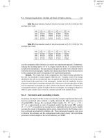
Register Addressing Modes
Indirect Addressing:
• Full 8 bit register address is written the special function register FSR
• INDF is used to get the content of the address pointed by FSR
• Exp : A sample program to clear RAM locations H’20’ – H’2F:
MOVLW 0x20 ;initialize pointer
MOVWF FSR ;to RAM
NEXT CLRF INDF ;clear INDF register
INCF FSR,F ;inc pointer
BTFSS FSR,4 ;all done?
GOTO NEXT ;no clear next
CONTINUE
: ;yes continue
Immediate Addressing:
Movlw H’0F’
Direct Addressing:
Uses 7 bits of 14 bit instruction to identify a register file address 8th and 9th
bit comes from RP0 and RP1 bits of STATUS register.
i.e. Z equ D’2’ ; Z=2
btfss STATUS, Z ; test if the 3rd bit of the STATUS register is set
PIC Family Control Registers
Uses a series of “Special Function Registers”
for controlling peripherals and PIC behaviors.
STATUS Bank select bits, ALU bits (zero, borrow,
carry)
INTCON Interrupt control: interrupt enables, flags,
etc.
OPTION_REG contains various control bits to
configure the TMR0 prescaler/WDT
postscaler ,the External INT Interrupt, TMR0
and the weak pull-ups on PORTB
Special Function Register
”STATUS Register“
Special Function Register
”INTCON Register“
PIC Peripherals
Each peripheral has a set of SFRs to control its
operation.
Different PICs have different on-board peripherals
Peripheral Features
5 Digital I/O Ports
Three timer/counter modules
Timer0: 8-bit timer/counter with 8-bit pre-scaler
Timer1: 16-bit timer/counter with pre-scaler, can be incremented during SLEEP
via external crystal/clock
Timer2: 8-bit timer/counter with 8-bit period register, pre-scaler and post-scaler
A 10-bit ADC with 8 inputs
Two Capture, Compare, PWM modules
Capture is 16-bit, max. resolution is 12.5 ns
Compare is 16-bit, max. resolution is 200 ns
PWM max. resolution is 10-bit
Synchronous Serial Port (SSP) with SPI™ (Master mode) and I2C™
(Master/Slave)
Universal Synchronous Asynchronous Receiver Transmitter (USART/SCI)
with 9-bit address detection
Parallel Slave Port (PSP) 8-bits wide, with external RD, WR and CS controls