design course vlsi lecture notes ch2
Bạn đang xem bản rút gọn của tài liệu. Xem và tải ngay bản đầy đủ của tài liệu tại đây (548.88 KB, 36 trang )
ECE 410, Prof. A. Mason Lecture Notes Page 2.1
ECE 410: VLSI Design
Course Lecture Notes
(Uyemura textbook)
Professor Andrew Mason
Michigan State University
ECE 410, Prof. A. Mason Lecture Notes Page 2.2
CMOS Circuit Basics
nMOS
gate
gate
drain
source
source
drain
pMOS
• CMOS = complementary MOS
– uses 2 types of MOSFETs
to create logic functions
•nMOS
•pMOS
• CMOS Power Supply
– typically single power supply
– VDD, with Ground reference
• typically uses single power supply
• VDD varies from 5V to 1V
•Logic Levels
– all voltages between 0V and VDD
– Logic ‘1’ = VDD
– Logic ‘0’ = ground = 0V
+
-
VDD
VDD
=
CMOS
logic
circuit
CMOS
logic
circuit
V
VDD
logic 1
voltages
logic 0
voltages
undefined
ECE 410, Prof. A. Mason Lecture Notes Page 2.3
Transistor Switching Characteristics
•nMOS
–switching behavior
• on = closed, when Vin > Vtn
– Vtn = nMOS “threshold voltage”
– Vin is referenced to ground, Vin = Vgs
• off = open, when Vin < Vtn
•pMOS
–switching behavior
• on = closed, when Vin < VDD - |Vtp|
– |Vtp| = pMOS “threshold voltage” magnitude
– Vin is referenced to ground, Vin = VDD-Vsg
• off = open, when Vin > VDD - |Vtp|
pMOS
nMOS
nMOS
Vgs > Vtn = on
+
Vgs
-
Vin
gate
drain
source
Vin
+
Vsg
-
gate
source
drain
pMOS
Vsg > |Vtp| = on
Vsg = VDD - Vin
Vout
Rule to Remember:
‘source’ is at
• lowest potential for nMOS
• highest potential for pMOS
ECE 410, Prof. A. Mason Lecture Notes Page 2.4
Transistor Digital Behavior
•nMOS
•pMOS
pMOS
nMOS
nMOS
V
g
s > Vtn = on
+
Vgs
-
Vin
gate
drain
source
Vin
+
Vsg
-
gate
source
drain
pMOS
Vsg > |Vtp| = on
Vsg = VDD - Vin
Vin
VDD
pMOS
nMOS
VDD-|Vtp|
Vtn
on
off
off
on
Vin Vout (drain)
1 Vs=0 device is ON
0 ? device is OFF
Vin Vout (drain)
1 ? device is OFF
0 Vs=VDD=1 device is ON
Vout
Vout
Notice:
When Vin = low, nMOS is off, pMOS is on
When Vin = high, nMOS is on, pMOS is off
Æ Only one transistor is on for each digital voltage
ECE 410, Prof. A. Mason Lecture Notes Page 2.5
MOSFET Pass Characteristics
nMOS
pMOS
Rule to Remember
‘source’ is at lowest potential for nMOS and at highest potential for pMOS
+
Vgs=Vtn
-
0 V
VDD
VDD
VDD
Vy = 0 V
Vy =
VDD-Vtn
-
Vsg=|Vtp|
+
VDD
0 V
0 V
0 V
Vy = VDD Vy = |Vtp|
ON when gate
is ‘low’
ON when gate
is ‘high’
Passes a good low
Max high is VDD-Vtn
Passes a good high
Min low is |Vtp|
• Pass characteristics: passing of voltage from drain (or source) to
source (or drain) when device is ON (via gate voltage)
• Each type of transistor is better than the other at passing (to
output) one digital voltage
– nMOS passes a good low (0) but not a good high (1)
– pMOS passes a good high (1) but not a good low (0)
?
?
?
?
ECE 410, Prof. A. Mason Lecture Notes Page 2.6
MOSFET Terminal Voltages
• How do you find one terminal voltage if the other 2 are known?
–nMOS
• case 1) if Vg > Vi + Vtn, then Vo = Vi (Vg-Vi > Vtn)
– here Vi is the “source” so the nMOS will pass Vi to Vo
• case 2) if Vg < Vi + Vtn, then Vo = Vg-Vtn (Vg-Vi < Vtn)
– here Vo is the “source” so the nMOS output is limited
–pMOS
• case 1) if Vg < Vi - |Vtp|, then Vo = Vi (Vi-Vg > |Vtp|)
– here Vi is the “source” so the pMOS will pass Vi to Vo
• case 2) if Vg > Vi - |Vtp|, then Vo = Vg+|Vtp| (Vi-Vg < |Vtp|)
– here Vo is the “source” so the pMOS output is limited
Vg
Vo
Vi
Vg
Vo
Vi
For nMOS, max(Vo) = Vg-Vtn
For pMOS, min(Vo) = Vg+|Vtp|
IMPORTANT:
Rules only apply if the devices is ON (e.g., Vg > Vtn for nMOS)
ECE 410, Prof. A. Mason Lecture Notes Page 2.7
MOSFET Terminal Voltages: Examples
–nMOSrules
• case 1) if Vg > Vi + Vtn, then Vo = Vi (Vg-Vi > Vtn)
• case 2) if Vg < Vi + Vtn, then Vo = Vg-Vtn (Vg-Vi < Vtn)
•nMOSexamples (Vtn=0.5V)
– 1: Vg=5V, Vi=2V
• Vg=5 > Vi +Vtn = 2.5 ⇒ Vo = 2V
– 2: Vg=2V, Vi=2V
• Vg=2 < Vi+Vtn = 2.5 ⇒ Vo = 1.5V
–pMOSrules
• case 1) if Vg < Vi - |Vtp|, then Vo = Vi (Vi-Vg > |Vtp|)
• case 2) if Vg > Vi - |Vtp|, then Vo = Vg+|Vtp| (Vi-Vg < |Vtp|)
•pMOSexamples (Vtp=-0.5V)
– 1: Vg=2V, Vi=5V
• Vg=2 < Vi-|Vtp|=4.5 ⇒ Vo = 5V
– 2: Vg=2V, Vi=2V
• Vg=2 > Vi-|Vtp|=1.5 ⇒ Vo = 2.5V
Vg
Vo
Vi
Vg
Vo
Vi
max(Vo) = Vg-Vtn
min(Vo) = Vg+|Vtp|
5
2
Vg
Vo
Vi
2
2
5
2
Vg
Vo
Vi
2
2
acts as
the source
acts as
the source
source
1.5
source
.5
2
52
ECE 410, Prof. A. Mason Lecture Notes Page 2.8
Switch-Level Boolean Logic
• Logic gate are created by using sets of controlled switches
• Characteristics of an assert-high switch
– y = x • A, i.e. y = x if A = 1
Series switches ⇒ AND function Parallel switches ⇒ OR function
nMOS acts like an
assert-high switch
AND, or multiply function
a AND b
a OR b
ECE 410, Prof. A. Mason Lecture Notes Page 2.9
Switch-Level Boolean Logic
• Characteristics of an assert-low switch
– y = x • A, i.e. y = x if A = 0
Series assert-low switches ⇒ ?
NOR
Remember This??
DeMorgan relations
a • b = a + b, a + b = a • b
a=1 ⇒ SW1 closed, SW2 open ⇒ y=0 = a
a=0 ⇒
SW1 open, SW2 closed ⇒ y=1 = a
NOT function, combining assert-
high and assert-low switches
y=x y=?
pMOS acts like an
assert-low switch
a b
error in figure 2.5
NOT (a OR b)
ECE 410, Prof. A. Mason Lecture Notes Page 2.10
CMOS “Push-Pull” Logic
• CMOS Push-Pull Networks
–pMOS
•“on”when input is low
• pushes
output high
–nMOS
•“on”when input is high
• pulls
output low
• Operation: for a given logic function
– one logic network (p or n) produces the logic function
and pushes or pulls the output
– the other network acts as a “load” to complete the
circuit, but is turned off by the logic inputs
– since only one network it active, there is no static
current (between VDD and ground)
•zero static power dissipation
pMOS
nMOS
assert-low
logic
inputs
output
assert-high
logic
ECE 410, Prof. A. Mason Lecture Notes Page 2.11
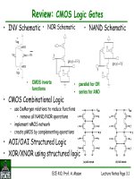
Creating Logic Gates in CMOS
• All standard Boolean logic functions (INV, NAND, OR, etc.) can be
produced in CMOS push-pull circuits.
• Rules for constructing logic gates using CMOS
– use a complementary nMOS/pMOS pair for each input
– connect the output to VDD through pMOS txs
– connect the output to ground through nMOS txs
– insure the output is always either high or low
• CMOS produces “inverting” logic
– CMOS gates are based on the inverter
– outputs are always inverted logic functions
e.g., NOR, NAND rather than OR, AND
• Logic Properties
assert-low
logic
inputs
output
assert-high
logic
nMOS
pMOS
Useful Logic Properties
1 + x = 1 0 + x = x
1 ⋅ x = x 0 ⋅ x = 0
x + x’ = 1 x ⋅ x’ = 0
a ⋅ a = a a + a = a
ab + ac = a (b+c)
DeMorgan’s Rules
(a ⋅ b)’ = a’ + b’
(a + b)’ = a’ ⋅ b’
Properties which can be proven
(a+b)(a+c) = a+bc
a + a'b = a + b
ECE 410, Prof. A. Mason Lecture Notes Page 2.12
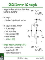
Review: Basic Transistor Operation
CMOS Circuit Basics
•nMOS
–0 in Æ 0 out
–VDD in Æ VDD-Vtn out
– strong ‘0’, weak ‘1’
•pMOS
–VDD in Æ VDD out
–0 in Æ |Vtp| out
– strong ‘1’, weak ‘0’
assert-low
logic
inputs
output
assert-high
logic
nMOS
Vgs > Vtn = on
+
Vgs
-
Vin
gate
drain
source
Vin
+
Vsg
-
gate
source
drain
pMOS
Vsg > |Vtp| = on
Vsg = VDD - Vin
nMOS
pMOS
Vin
VDD
pMOS
nMOS
Vtn
on
off
off
on
+
Vgs=Vtn
-
0 V
VDD
VDD
VDD
Vy = 0 V
Vy =
VDD-Vt
n
-
Vsg=|Vtp|
+
VDD
0 V
0 V
0 V
Vy = VDD Vy = |Vtp|
CMOS Pass Characteristics
nMOS
pMOS
‘source’ is at lowest potential (nMOS) and highest potential (pMOS)
VDD-|Vtp|
Vg=
Vin
Vout
?
0
0
1
Vg=
Vin
Vout
1
?
0
1
off = open
on = closed
on = closed
off = open
ECE 410, Prof. A. Mason Lecture Notes Page 2.13
Review: Switch-Level Boolean Logic
• assert-high switch
– y = x • A, i.e. y = x if A = 1
– series = AND
– parallel = OR
• assert-low switch
– y = x • A, i.e. y = x if A = 0
– series = NOR
– parallel = NAND
a b
=x
a AND b
a OR b
NOT (a OR b)
ECE 410, Prof. A. Mason Lecture Notes Page 2.14
• Inverter Symbol
• Inverter Truth Table
• Inverter Function
• toggle binary logic of a signal
• Inverter Switch Operation
CMOS Inverter
+
Vgs
-
Vout
Vin
pMOS
nMOS
+
Vsg
-
=VDD
Vin=VDD
x y
= Vin
xy
0
1
1
0
= x
input low Æ output high
nMOS off/open
pMOS on/closed
• CMOS Inverter Schematic
input high Æ output low
nMOS on/closed
pMOS off/open
pMOS “on”
Æ output high (1)
nMOS “on”
Æ output low (0)
ECE 410, Prof. A. Mason Lecture Notes Page 2.15
nMOS Logic Gates
• We will look at nMOS logic first, more simple than CMOS
• nMOS Logic (no pMOS transistors)
– assume a resistive load to VDD
– nMOS switches pull output low based on inputs
c = a+b
c = ab
nMOS Inverter
(a) nMOS is off
Æ output is high (1)
(b) nMOS is on
Æ output is low (0)
nMOS NOR nMOS NAND
• parallel switches = OR function
• nMOS pulls low (NOTs the output)
• series switches = AND function
• nMOS pulls low (NOTs the output)
VDD VDD
=VDD
VDD
ECE 410, Prof. A. Mason Lecture Notes Page 2.16
CMOS NOR Gate
• NOR Symbol
• Karnaugh map
xy
0
0
1
1
0
1
0
1
x+y
• NOR Truth Table
x
y
x + y
1
0
0
0
y 0 1
x
0
1
1 0
0 0
g(x,y) = x • y • 1 + x • 0 + y • 0
• construct Sum of Products equation with all terms
• each term represents a MOSFET path to the
output
• ‘1’ terms are connected to VDD via pMOS
• ‘0’ terms are connected to ground via nMOS
“true” terms “false” terms
ECE 410, Prof. A. Mason Lecture Notes Page 2.17
CMOS NOR Gate
• Notice: series-parallel arrangement
– when nMOS in series, pMOS in parallel, and visa versa
– true for all
static CMOS
logic gates
– allows us to construct more complex logic functions
• CMOS NOR Schematic
• output is LOW if x OR y is true
• parallel nMOS
• output is HIGH when x AND y are false
• series pMOS
g(x,y) = x • y • 1 + x • 0 + y • 0
x
x
y
g(x,y) = x + y
ECE 410, Prof. A. Mason Lecture Notes Page 2.18
CMOS NAND Gate
•NAND Symbol
• CMOS Schematic
xy
0
0
1
1
0
1
0
1
x•y
•Truth Table
x
y
x • y
1
1
1
0
y 0 1
x
0
1
1 1
1 0
g(x,y) = (y•1) + (x•1) + (x • y • 0)
•K-map
• output is LOW if x AND y are true
• series nMOS
• output is HIGH when x OR y is false
• parallel pMOS
x
x
y
g(x,y) = x y
ECE 410, Prof. A. Mason Lecture Notes Page 2.19
3-Input Gates
•NOR3
•NAND3
x
y
z
x+y+z
x
y
x
y
z
g(x,y) = x+y+z
•Alternate Schematic
• what function?
• note shared gate inputs
• is input order important?
• in series, parallel, both?
• this schematic resembles how the
circuit will look in
physical layout
x
y
z
x y z
xy
y
x
z
g(x,y) = x y z
x
yz
ECE 410, Prof. A. Mason Lecture Notes Page 2.20
Complex Combinational Logic
• General logic functions
–for example
• How do we construct the CMOS gate?
– use DeMorgan principles to modify expression
• construct nMOS and pMOS networks
– use Structured Logic (covered only briefly in ECE410)
•AOI (AND OR INV)
• OAI (OR AND INV)
f = a • (b + c), f = (d • e) + a • (b + c)
a • b = a + b a + b = a • b
ECE 410, Prof. A. Mason Lecture Notes Page 2.21
Using DeMorgan
•DeMorganRelations
–NAND-OR rule
• bubble pushing illustration
• bubbles = inversions
–NOR-AND rule
a + b = a • b
x
y
equivalent
to
x
y
x + y
x y
a • b = a + b
x
y
equivalent
to
x
y
x + y
x y
• pMOS and bubble pushing
– Parallel-connected pMOS
• assert-low OR
• creates NAND function
– Series-connected pMOS
• assert-low AND
•creates NOR function
x
y
x + y
yx
g(x,y) = x + y = x y
x
x
y
x y
y
g(x,y) = x y = x + y
to implement pMOS this way, must push all bubbles
to the inputs and remove all NAND/NOR output bubbles
ECE 410, Prof. A. Mason Lecture Notes Page 2.22
Review: CMOS NAND/NOR Gates
•NOR Schematic
• output is LOW if x AND y are true
• series nMOS
• output is HIGH when x OR y is false
• parallel pMOS
x
x
y
g(x,y) = x y
x
x
y
g(x,y) = x + y
•NAND Schematic
• output is LOW if x OR y is true
• parallel nMOS
• output is HIGH when x AND y are false
• series pMOS
ECE 410, Prof. A. Mason Lecture Notes Page 2.23
Rules for Constructing CMOS Gates
• Given a logic function
F = f(a, b, c)
• Reduce (using DeMorgan) to eliminate inverted operations
– inverted variables are OK, but not operations (NAND, NOR)
• Form pMOS network by complementing the inputs
Fp = f(a, b, c)
• Form the nMOS network by complementing the output
Fn = f(a, b, c) = F
• Construct Fn and Fp using AND/OR series/parallel
MOSFET structures
– series = AND, parallel = OR
x
x
y
g(x,y) = x y
The Mathematical Method
EXAMPLE:
F = ab ⇒
Fp = a b = a+b; OR/parallel
Fn = ab = ab; AND/series
ECE 410, Prof. A. Mason Lecture Notes Page 2.24
CMOS Combinational Logic Example
• Construct a CMOS logic gate to implement the function:
F = a • (b + c)
•pMOS
– Apply DeMorgan expansions
F = a + (b + c)
F = a + ( b • c )
– Invert inputs for pMOS
Fp = a + (b • c)
– Resulting Schematic
a
F
b
c
•nMOS
– Invert output for nMOS
Fn = a • (b + c)
– Apply DeMorgan
none needed
– Resulting Schematic
a
bc
F=a(b+c)
a
a
b
b
c
c
F=a(b+c)
ab
c
F=a(b+c)
14 transistors (cascaded gates)
6 transistors
(CMOS)
ECE 410, Prof. A. Mason Lecture Notes Page 2.25
Structured Logic
• Recall CMOS is inherently Inverting logic
• Can used structured circuits to implement general logic
functions
•AOI:implements logic function in the order
AND, OR, NOT (Invert)
–Example: F = a •b + c •d
• operation order: i) a AND b, c AND d, ii) (ab) OR (cd), iii) NOT
– Inverted Sum-of-Products (SOP) form
•OAI:implements logic function in the order
OR, AND, NOT (Invert)
–Example: G = (x+y) • (z+w)
• operation order: i) x OR y, z OR w, ii) (x+y) AND (z+w), iii) NOT
– Inverted Product-of-Sums (POS) form
• Use a
structured CMOS array
to realize such functions