design course vlsi lecture notes ch3-5
Bạn đang xem bản rút gọn của tài liệu. Xem và tải ngay bản đầy đủ của tài liệu tại đây (4.76 MB, 69 trang )
ECE 410, Prof. A. Mason Lecture Notes Page 3.1
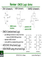
Review: CMOS Logic Gates
• NOR Schematic
x
x
y
g(x,y) = x y
x
x
y
g(x,y) = x + y
•NAND Schematic
• parallel for OR
• series for AND
• INV Schematic
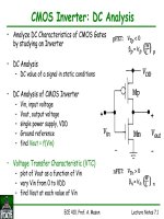
+
Vgs
-
Vout
Vin
pMOS
nMOS
+
Vsg
-
= Vin
• CMOS inverts
functions
• CMOS Combinational Logic
• use DeMorgan relations to reduce functions
• remove all NAND/NOR operations
• implement nMOS network
• create pMOS by complementing operations
• AOI/OAI Structured Logic
• XOR/XNOR using structured logic
ECE 410, Prof. A. Mason Lecture Notes Page 3.2
Review: XOR/XNOR and TGs
•Exclusive-OR (XOR)
–a ⊕ b = a • b + a • b
•Exclusive-NOR
–a ⊕ b = a • b + a • b
• Transmission Gates
• MUX Function using TGs
b
a
b
a
XOR/XNOR in AOI Form
y = x s, for s=1
F = Po • s + P1 • s
ECE 410, Prof. A. Mason Lecture Notes Page 3.3
CMOS Technology
• Properties of microelectronic materials
– resistance, capacitance, doping of semiconductors
• Physical structure of CMOS devices and circuits
– pMOS and nMOS devices in a CMOS process
– n-well CMOS process, device isolation
• Fabrication processes
• Physical design (layout)
– layout of basic digital gates, masking layers, design rules
–LOCOS process
– planning complex layouts (Euler Graph and Stick Diagram)
Part I: CMOS Technology
ECE 410, Prof. A. Mason Lecture Notes Page 3.4
Integrated Circuit Layers
• Integrated circuits are a stack of patterned layers
– metals, good conduction, used for interconnects
– insulators (silicon dioxide), block conduction
– semiconductors (silicon), conducts under certain conditions
• Stacked layers form 3-dimensional structures
• Multi-layer metals
– background assumed to be
silicon covered by silicon dioxide
silicon
silicon
dioxide
Part I: CMOS Technology
ECE 410, Prof. A. Mason Lecture Notes Page 3.5
Interconnect Parasitics
• Parasitic = unwanted natural electrical elements
• Metal Resistance
– metals have a linear resistance and obey Ohm’s law
•V = IR
– generate parasitic interconnect resistance, R
line
•R
line
=
l
= ρ
l
–A =
wt
– ρ = resistivity, σ = conductivity
– defined by sheet resistance
• Rs = 1 = ρ , resistance per unit length [ohms, Ω]
•Rline= Rs
l
, Rs determined by process,
l
&
w
by designer
σA
A
l
t
w
σ
t t
w
Rline = Rs
when
l = w
Part I: CMOS Technology
ECE 410, Prof. A. Mason Lecture Notes Page 3.6
Metal Resistance: Measuring ‘squares’
• From top view of layout, can determine how many
‘squares’ of the layer are present
– ‘square’ is a unit length equal to the width
–R
line
= Rs n, where n =
l
is the number of ‘squares’
– Get a unit of resistance, Rs, for each square, n.
l
w
w
w
n = 8
Part I: CMOS Technology
ECE 410, Prof. A. Mason Lecture Notes Page 3.7
Parasitic Line Capacitances
• Capacitor Basics
–Q = CV, C in units of Farads [F]
–I = C
d
V/
d
t
• Parallel plate capacitance
–C
line
= ε
ox
wl
[F], w l = Area
– ε
ox
= permittivity of oxide
• ε
ox
= 3.9 ε
o
• ε
o
= 8.85X10
-14
[F/cm]
•RC time constant of
an interconnect line
– τ
= R
line
C
line
t
ox
Part I: CMOS Technology
ECE 410, Prof. A. Mason Lecture Notes Page 3.8
Electrical Properties of Silicon
• Silicon is a semiconductor… does it conduct or insulate?
–doping= adding impurities (non-silicon) to Si:
will be covered later
• doping concentration and temperature determine resistivity
• Conduction/Resistance
– generally, the Si we see in CMOS is doped
• at room temp., doped silicon is a weak conductor = high resistance
• Capacitance
– doped, room temp. Si is conductive
–conduction Æ free charge carriers Æ no electric field
Æ no capacitance (within bulk silicon)
– exception: if free carries are removed (e.g., depletion layer of a
diode) silicon becomes an insulator with capacitance
Part I: CMOS Technology
ECE 410, Prof. A. Mason Lecture Notes Page 3.9
Conduction in Semiconductors -Review
• Intrinsic (undoped) Semiconductors
– intrinsic carrier concentration ≡ n
i
= 1.45x10
10
cm
-3
, at room temp.
– n = p = n
i
, in intrinsic (undoped) material
•n ≡ number of electrons, p ≡ number of holes
– mass-action law, np = n
i
2
applies to undoped and doped material
• Extrinsic (doped) Semiconductors
– dopants added to modify material/electrical properties
P
BP
B
+
+
+
+
-
-
group V
element
group III
element
ion
electron
hole
n-type Donor
p-type Acceptor
ion
free
carrier
free
carrier
•n-type (n+), add elements with extra an electron
–N
d
≡ conc. of donor atoms [cm
-3
]
–n
n
= N
d
, n
n
≡ conc. of electrons in n-type material
–p
n
= n
i
2
/N
d
, using mass-action law,
–p
n
≡ conc. of holes in n-type material
–always a lot more n than p in n-type material
•p-type = p+, add elements with an extra hole
–N
a
≡ concentration of acceptor atoms [cm
-3
]
–p
p
= N
a
, p
p
≡ conc. of holes in p-type material
–n
p
= ni
2
/N
a
, using mass-action law,
–n
p
≡ conc. of electrons in p-type material
–always a lot more p than n in p-type material
Part I: CMOS Technology
ECE 410, Prof. A. Mason Lecture Notes Page 3.10
Conduction in Silicon Devices
• doping provides free charge carriers, alters conductivity
• conductivity in semic. w/ carrier densities n and p
– σ = q(μ
n
n + μ
p
p)
•q≡ electron charge, q = 1.6x10
-19
[Coulombs]
• μ≡mobility [cm
2
/V-sec], μ
n
≅ 1360, μ
p
≅ 480 (typical values in
bulk
Si)
• in n-type region, n
n
>> p
n
– σ≈qμ
n
n
n
• in p-type region, p
p
>> n
p
– σ≈qμ
p
p
p
• resistivity, ρ = 1/σ
• Can now calculate the resistance of an n+ or p+ region
μ
n
> μ
p
electrons more mobile than holes
conductivity of n+ > p+
Mobility often assumed constant
but is a function of Temperature and
Doping Concentration
Part I: CMOS Technology
ECE 410, Prof. A. Mason Lecture Notes Page 3.11
MOSFET Gate Operation
• Gate Capacitance
– gate-substrate
parallel plate
capacitor
–C
G
= ε
ox
A/t
ox
[F]
• ε
ox
= 3.9 ε
o
• ε
o
= 8.85X10
-14
[F/cm]
• Oxide Capacitance
–Cox = ε
ox
/t
ox
[F/cm
2
]
–C
G
= Cox A
G
[F]
•A
G
=gate area = L•W [cm
2
]
• Charge on Gate, +Q, induces
charge -Q in substrate channel
– channel charge allows conduction
between source and drain
channel = substrate
region under the gate,
between S and D
Part I: CMOS Technology
ECE 410, Prof. A. Mason Lecture Notes Page 3.12
Physical n/pMOS Devices
• nMOS and pMOS cross-section
•Layers
– substrate, n-well, n+/p+ S/D, gate oxide,
polysilicon gate, S/D contact, S/D metal
• Can you find all of the diodes (pn junctions)?
– where? conduct in which direction? what purpose?
lightly doped
p region
lightly
doped
n region
highly
doped
n region
highly
doped
p region
Part I: CMOS Technology
ECE 410, Prof. A. Mason Lecture Notes Page 3.13
Lower CMOS Layers
• Visible Features
–p-substrate
–n-well
– n+ S/D regions
– p+ S/D regions
–gate oxide
– polysilicon gate
•Mask Layers
–n-well
–active(S/D regions)
• active = not FOX
–n+doping
–p+doping
–polypatterning
• gate oxide aligned to gate poly, no oxide mask
poly
n-well
n+
p+
active
Part I: CMOS Technology
ECE 410, Prof. A. Mason Lecture Notes Page 3.14
Physical Realization of a 4-Terminal MOSFETs
•nMOS Layout
– gate is intersection of Active, Poly, and nSelect
– S/D formed by Active with Contact to Metal1
– bulk connection formed by p+ tap to substrate
•pMOSLayout
– gate is intersection of Active, Poly, and pSelect
– S/D formed by Active with Contact to Metal1
– bulk connection formed by n+ tap to nWell
• Active layer
– in lab we will use
nactive
and
pactive
• nactive should always be covered by nselect
• pactive should always be covered by pselect
– nactive and pactive are the same mask layer (active)
• different layout layers help differentiate nMOS/pMOS
Gate
D
SBulk
Ground
Gate
D
S
Bulk
VDD
Part I: CMOS Technology
ECE 410, Prof. A. Mason Lecture Notes Page 3.15
CMOS Device Dimensions
• Physical dimensions of a MOSFET
–L = channel length
–W = channel width
• Side and Top views
Part I: CMOS Technology
ECE 410, Prof. A. Mason Lecture Notes Page 3.16
Upper CMOS Layers
• Cover lower layers with oxide insulator, Ox1
• Contacts through oxide, Ox1
– metal1 contacts to
poly and active
•Metal 1
•Insulator Ox2
•Via contacts
•Metal 2
• Repeat insulator/via/metal
• Full Device Illustration
– active
–poly gate
– contacts (active & gate)
–metal1
–via
–metal2
only Metal 1 has
direct contact
to lower layers
Part I: CMOS Technology
ECE 410, Prof. A. Mason Lecture Notes Page 3.17
CMOS Cross Section View
• Cross section of a 2 metal, 1 poly CMOS process
• Layout (top view) of the devices above (partial, simplified)
Typical MOSFET Device (nMOS)
Part I: CMOS Technology
ECE 410, Prof. A. Mason Lecture Notes Page 3.18
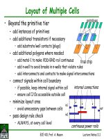
Inverter Layout
•Features
– VDD & Ground ‘rail’
• using Metal1 layer
–N-well region
•for pMOS
–Active layers
• different n+ and p+
–Contacts
• n+/p+ to metal
• poly to metal
• Alternate layout
–advantage
• simple poly routing
– disadvantage
• harder to make W large
vertical
poly
horizontal
poly
Part II: Layout Basics
ECE 410, Prof. A. Mason Lecture Notes Page 3.19
CMOS Layout Layers
• Mask layers for 1 poly,
2 metal, n-well CMOS process
– Background: p-substrate
–nWell
–Active
(nactive and pactive)
–Poly
–pSelect
–nSelect
–Active Contact
–Poly Contact
–Metal1
–Via
–Metal2
–Overglass
• See supplementary power point file for animated CMOS process flow
– should be viewed as a slide show, not designed for printing
Part II: Layout Basics
ECE 410, Prof. A. Mason Lecture Notes Page 3.20
Series MOSFET Layout
•Series txs
– 2 txs share a S/D junction
• Multiple series transistors
– draw poly gates side-by-side
Part II: Layout Basics
ECE 410, Prof. A. Mason Lecture Notes Page 3.21
Parallel MOSFET Layout
• Parallel txs
– one shared S/D junction with contact
– short other S/D using interconnect layer (metal1)
• Alternate layout strategy
– horizontal gates
Part II: Layout Basics
ECE 410, Prof. A. Mason Lecture Notes Page 3.22
NAND/NOR Layouts
• One layout option with horizontal transistors
(L runs horizontally)
– ignore the size (W) for now
2-input NAND
pMOS
2 parallel tx
nMOS
2 series txs
2-input NOR
pMOS
2 series tx
nMOS
2 parallel txs
Part II: Layout Basics
ECE 410, Prof. A. Mason Lecture Notes Page 3.23
Layout Cell Definitions
• Cell Pitch = Height of standard cells
measured between VDD & GND rails
–A: 410 lab definition
• top of VDD to bottom of GND
– B: interior size, without power rails
– C: textbook definition
• middle of GND to middle of VDD
• Cell Boundary
max extension of any layer (except nwell)
– set boundary so that cells can be placed
side-by-side without any rule violations
– extend power rails 1.5λ (or 2λ to be safe)
beyond any active/poly/metal layers
– extend n-well to cell boundary (or
beyond) to avoid breaks in n-well
VDD!
GND!
A
BC
VDD!
GND!
cell boundary
Part II: Layout Basics
ECE 410, Prof. A. Mason Lecture Notes Page 3.24
Cell Layout Guidelines
•Internal Routing
– use lowest routing layer possible, typically poly and metal1
– keep all possible routing inside power rails
– keep interconnects as short as possible
• Bulk (substrate/well) Contacts
– must have many contacts to p-substrate and n-well
• at least 1 for each connection to power/ground rails
– consider how signals will be routed in/out of the cells
• don’t block access to I/O signals with substrate/well contacts
•S/D Area Minimization
– minimize S/D junction areas to keep capacitance low
•I/O Pads
– Placement: must be able to route I/O signals out of cell
– Pad Layer: metal1
for smaller cells, metal2 acceptable in larger cells
•Cell Boundary
– extend VDD and GND rail at least 1.5λ beyond internal features
– extend n-well to cell boundary to avoid breaks in higher level cells
Part II: Layout Basics
ECE 410, Prof. A. Mason Lecture Notes Page 3.25
Layout CAD Tools
• Layout Editor
– draw multi-vertices polygons which represent physical design layers
– Manhattan geometries, only 90º angles
• Manhattan routing: run each interconnect layer perpendicular to each other
• Design Rules Check (DRC)
– checks rules for each layer (size, separation, overlap)
–
must pass DRC or will fail in fabrication
• Parameter Extraction
– create netlist of devices (tx, R, C) and connections
– extract parasitic Rs and Cs, lump values at each line (R) / node (C)
• Layout Vs. Schematic (LVS)
– compare layout to schematic
– check devices, connections, power routing
• can verify device sizes also
– ensures layout matches schematic exactly
–
passing LVS is final step in layout
Part II: Layout Basics