design course vlsi lecture notes ch11
Bạn đang xem bản rút gọn của tài liệu. Xem và tải ngay bản đầy đủ của tài liệu tại đây (445.2 KB, 43 trang )
ECE 410, Prof. A. Mason Lecture Notes 11.1
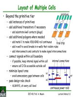
Layout of Multiple Cells
• Beyond the primitive tier
– add instances of primitives
– add additional transistors if necessary
• add substrate/well contacts (plugs)
– add additional polygons where needed
• add metal-1 to make VDD/GND rail continuous
• add n-well to avoid breaks in n-wells that violate rules
• add interconnects and contacts to make signal interconnections
– connect signals within cell boundary
• if possible, keep internal signal within cell
• ensure cell I/Os accessible outside cell
– minimize layout area
• avoid unnecessary gaps between cells
– pass design rule check
• ALWAYS, at every cell level
final chip
primitives
internal connections
in1
continuous power rails
in2
out
ECE 410, Prof. A. Mason Lecture Notes 11.2
Multi-Instance Cells
• Cell Placement
– pack cells side-by-side
• abut cells and align power rails
– avoid gaps between cells
• unless needed for signal connections
• Signal Routing
– make internal connections using poly and metal-1, if possible
– use jumpers outside rails only when necessary
• jump up/down using poly (short trace) or metal-2 (if long trace)
– poly for traces close to cell
– metal-2 for traces far from cell
• leave room for widened power rails
• Power Routing
– more cells mean more supply current
– widen power supply rail for long
cascades of cells
internal connections
in1
continuous power rails
in2
ou
t
widened power supply rails
signal jumpers
single cell cell cascade
X
X
X
X
X
X
X
cell B
cell C
cell A
ECE 410, Prof. A. Mason Lecture Notes 11.3
High-Level Layout
• Cell Placement
– cascade cells with same pitch
– stack cascaded cells
• Cell Orientation
– maintain orientation when stacking
• signal jumpers between stacks
or
–alternate orientation
• signal jumpers on top and/or bottom
• Power Routing
– widen supply rails for long cascades
– connect rails outside cell cascades
• example follows
cell
cascade
VDD
GND
jumpers
VDD
GND
jumpers
VDD
GND
GND
VDD
jumpers
ECE 410, Prof. A. Mason Lecture Notes 11.4
• General Rules
– use lowest level interconnects possible
• if process has less than ~3 metal layers
– try to route a cell cascade using only poly and metal-1
• if process has more than ~3 metals
– route cell cascade using metal-1 and metal-2, avoid using poly
– alternate directions for each interconnect
• e.g., metal1 horizontally, metal2 vertically, metal 3 horizontally, etc.
•Example
• Note: new process technologies have specially defined metal layers
• e.g. metal_5 might be dedicated to VDD routing
poly
• within primitives
• local interconnects
•only if <3 metal layers
metal1
• within primitives
•power rails
• horizontal jumpers
metal2
• vertical traces between stacked cascades
Metal Routing Strategy
ECE 410, Prof. A. Mason Lecture Notes 11.5
Power Routing
• Power Rails for Combined Cells
– join adjacent cells with continuous power rails
– keep power rails wide enough for long power traces
• more cells Æ more current Æ need traces with lower resistance
– power tree concept
• power enters chip on one pin
• must “branch” across chip
• traces should be thicker near pin
and narrow into smaller cells
• Connecting rails in stacked cell cascades
branching of power traces across a chip,
from thick lines (chip) to thin lines (cell)
GND VDD
use
many
contacts
(vias)
jumper area
jumper area
VDD
GND
VDD
GND
VDD
GND
cell cascadecells
pin
chip-level
cell-level
zooming
out…
VDD
GND metal1
metal2
ECE 410, Prof. A. Mason Lecture Notes 11.6
Signal Buffers
• Loading and Fan-Out
– gate input capacitance
•C
G
= 2CoxWL (1 for pMOS 1 for nMOS)
– load capacitance
• standard gate designed to drive a load of 3 gates Æ C
L
= 3C
G
– output drive capability
•I ∝ W, increase W for more output signal drive
• increasing W increase C
G
• Buffers
– single stage inverter buffers
• isolate internal signals from output load
– scaled inverter buffers
• add drive strength to a signal
• inverters with larger than minimum tx
– typically increase by 3x at with each stage
min.
W/L
3W/L 9W/L 27W/L
1x 3x 9x 27x
drive
81C
G
drive
3C
G
drive
9C
G
drive
27C
G
input cap.
C
G
3C
G
9C
G
27C
G
ECE 410, Prof. A. Mason Lecture Notes 11.7
Transmission Gate Multiplexors
• Logical Function of a Multiplexor
– select one output from multiple inputs
– 2:1 MUX logic
• CMOS Multiplexors
– generally formed using switch logic rather than static
• 2:1 MUX using Transmission Gates
• 4:1 MUX using 2:1 MUXs
ECE 410, Prof. A. Mason Lecture Notes 11.8
Pass-gate Multiplexors
• 2:1 MUX using pass-gates
– nMOS switch circuit
• 4:1 MUX using pass-gates
• Pass-gate MUX with
rail-to-rail output
– add full pMOS network
• see Figure 11.7 in textbook
•Multi-bit MUXs
– use parallel single-bit MUXs
buffer for
output drive
ECE 410, Prof. A. Mason Lecture Notes 11.9
Binary Decoders
• Decoder Basic Function
–
n
bits can be decoded into
m
values
•max
m
is 2
n
– decoded values are active only one at a time
• active high: only selected value is logic 1
• active low: only selected value is logic 0
•Example: 2/4 (
2-to-4
) Decoder
– 2 control bits decoded into 4 values
•truth table
• equations
– active high decoder equations require NOR operation
control
inputs
active high
decoded outputs
control inputs select
one active output
n select bits decode into
2
n
outputs values
ECE 410, Prof. A. Mason Lecture Notes 11.10
CMOS Decoder Circuits
• 2/4 Active High Decoder
• 2/4 Active Low Decoder
– implemented with NAND gates
• Similar approach for higher-value decoders
Truth Table Symbol
Truth Table Symbol
NAND2 Circuit
active low
2/4 decoder
NOR2 Circuit
active high
2/4 decoder
3/8 decoder requires 3-input gates, higher values get complex
ECE 410, Prof. A. Mason Lecture Notes 11.11
Transmission Gate Decoders
• EXAMPLE: 3/8 Active-High Decoder
– each output connected to VDD
through 3 transmission gates
– TG selects set to turn on only one of
the 8 possible combinations of the 3-
bit select
• What do the resistors at output do?
• What is the signal value at the
unselected outputs?
s2 s1 s0 d7 d6 d5 d4 d3 d2 d1 d0
000 1
001 1
010 1
011 1
100 1
101 1
110 1
1111
ECE 410, Prof. A. Mason Lecture Notes 11.12
Magnitude Comparators
• Often need to compare the value of 2 n-bit numbers
– EQUAL if values are the same
– GREATER THAN if a is greater than b
– LESS THAN if b is greater than a
• Equality: a_EQ_b, can be generated by XNOR operation
– a = b iff aXNORb = 1 for each binary digit
• example: 4b equality comparator using XNOR
– also, a=b if a>b=0 and a<b=0 for ach binary digit
• Greater/Less Than, by bit-by-bit comparison
a_EQ_b
4b GT, LT Logic
4b Equality Circuit
note: can get Equal
from GT, LT circuit
ECE 410, Prof. A. Mason Lecture Notes 11.13
Combined Comparator Circuits
• 8b Magnitude Comparator with Output Enable
– generates, EQ (equal), GT (greater than), LT (less than)
4-bit
comparator
from
previous
page
compares outputs from 4b cells,
implements Enable,
produces 8b compare results
ECE 410, Prof. A. Mason Lecture Notes 11.14
Priority Encoders
• Priority Encoders generates an encoded result showing
–IF a binary number has a logic 1 in any bit
– WHERE the most significant logic 1 occurs
• Output is an encoded value of the location of the most
significant ‘1’
• Example: 8b priority encoder
• Outputs can be constructed from the truth table
– see textbook for illustrations of CMOS logic
assign d
7
highest priority,
d
0
lowest
Q
2
-Q
0
encode the value of
the highest priority 1
Q
3
is high if any bit in d is logic 1
ECE 410, Prof. A. Mason Lecture Notes 11.15
Data Latches
• Latch Function
– store a data value
• non-volatile; will not lose value over time
– often incorporated in static memory
– building block for a master-slave flip flop
• Static CMOS Digital Latch
– most common structure
• cross-coupled inverters, in positive feedback arrangement
– circuit forces itself to maintain data value
• inverter
a
outputs a 1 causing inverter
b
to output a 0
• or, inverter
a
outputs a 0 causing inverter
b
to output a 1
Bistable
circuit
Latches also improve signal
noise immunity; feedback
forces signal to hold value
and filters noise
ECE 410, Prof. A. Mason Lecture Notes 11.16
D-Latch Logic Circuit
• Accessing Latch to Set Value
– apply input D to set latched value
• NOR D-Latch
– uses NOR cells to create latch function
• D-Latch with Enable
–En selects if output
• set by input, D
• or from internal
feedback
• Different structures used in VLSI
Transistor-Level
Circuit
Logic-Level
Circuit
ECE 410, Prof. A. Mason Lecture Notes 11.17
CMOS VLSI Clocked Latches
• Clocked (enable) Latch using TGs
– can use TGs to determine
• if latch sees D
–C = 1 ⇒ Q’ = D’, set data mode
• or if positive feedback is applied
–C = 0 ⇒ Q’ = Q’, hold data mode
• Reducing Transistor Count
– Single TG D-Latch
• input must overdrive feedback signal
– must use weak feedback inverter
• useful when chip area is critical
– but input signal must be strong
– Pass-gate D-Latch
• replace TG with nMOS Pass-gate
• very common VLSI latch circuit
ECE 410, Prof. A. Mason Lecture Notes 11.18
Flip Flop Basics
• storage element for synchronous circuits
– save logic state at each clock cycle
• 1 or 2 signal inputs and a
clock
• differential outputs, Q and Q’
– output changes on rising (or falling) clock edge
– output held until next rising (or falling) clock edge
•optional asynchronous
set
and/or
reset
– regardless of clock state, output set (1) or reset (0)
• typically
master-slave
circuit using 2 cascaded latches
•types include
–JK
– T (toggle)
– SR (set-reset)
–D -most common for ICs
Flip-flop symbol (SR) for rising
and falling edge clocks
ECE 410, Prof. A. Mason Lecture Notes 11.19
Types of Flip Flops
•D-type (DFF)
• SR-type
same as D if S=D and R=D’
•JK-type
NOTE: Circuit based on
standard logic gates is
typically much larger
than possible with a
reduced CMOS circuit
ECE 410, Prof. A. Mason Lecture Notes 11.20
JK and T Flip Flops from DFF
• D-Flip Flop can be used to create most other FF types
• Can construct a JK FF from a DFF
• T-type (toggle) FF can be constructed from a JK FF
–T=1
• output changes state on each clock cycle
–T=0
• hold output to previous value
– form from JK by connecting J and K inputs together as T
ECE 410, Prof. A. Mason Lecture Notes 11.21
Master-Slave D Flip Flop
• D-type master-slave flip flop is the most common in VLSI
• Master-Slave Concept
– cascade 2 latches clocked on opposite clock phases
• φ = 1, φ = 0: D passes to master, slave holds previous value
• φ = 0, φ = 1 : D is blocked from master, master holds value and
passes value to slave
• Triggering
– Output only changes on clock edge; output is held when clock is at a
level value (0 or 1)
– Positive Edge
• output changes only on rising edge of clock
– Negative Edge
• output changes only on falling edge of clock
ECE 410, Prof. A. Mason Lecture Notes 11.22
Set/Reset Flip Flops
• Asynchronous Set and Reset
– Asynchronous = not based/linked to clock signal
– Typically negative logic
(0=active, 1=inactive)
–Set: forces Q to logic 1
–Reset: forces Q to logic 0
•Logic Diagrams
– DFFR
•with Reset (clear)
– DFFRS
•with Reset (clear) and Set
X
10
0
0
1
X
1
0
X
Alternate logic structure
ECE 410, Prof. A. Mason Lecture Notes 11.23
Buffering in Flip Flops
• What is a buffer?
– inverter buffers
• isolate output load from internal signals
– scaled inverter buffers
• add drive strength to a signal
• inverters with larger than minimum tx
– typically increase by 3x at with each stage
• Inter-cell Buffering
–Clock
• so each flip flop provide only
1 C
G
load on input CLK
–Output
• so load at output won’t affect
internal operation of the cell
D
CLK
Q
φ
φ
φ
φ
Q
φ
φ
min.
W/L
3W/L 9W/L 27W/L
1x 3x 9x 27x
drive
81C
G
drive
3C
G
drive
9C
G
drive
27C
G
input cap.
C
G
3C
G
9C
G
27C
G
Example: Buffers in the Lab 7 DFF cell
ECE 410, Prof. A. Mason Lecture Notes 11.24
Characterizing Flip Flop Timing
•Setup Time: t
su
– Time D must remain stable before the clock
changes
•Hold Time: t
h
– Time D must remain stable after the clock changes
•Clock to Q Time: t
c2q
– Time from the clock edge until the correct
value appears at Q
ECE 410, Prof. A. Mason Lecture Notes 11.25
Analyzing DFF Timing
•Setup
–When φ is low D must
propagates through both
master inverters, if clock
changes before then the
master may switch
–t
su
= t
M1
+ t
I1
+ t
I2
•Hold
– As soon as φ is goes high, D is
cutoff
–t
h
= 0
•Clock to Q
– For both outputs to be valid
must wait for both slave
inverters to change.
–t
c2Q
= t
M3
+ t
I2
+ t
I3
I1
I2
I3
I4
Different types of flip flops
exhibit different timing characteristics