thermal conductivity of bismuth telluride nanowire array epoxy composite
Bạn đang xem bản rút gọn của tài liệu. Xem và tải ngay bản đầy đủ của tài liệu tại đây (194.65 KB, 4 trang )
Birck Nanotechnology Center
Birck and NCN Publications
Purdue Libraries Year 2009
Thermal conductivity of bismuth
telluride nanowire array-epoxy composite
Kalapi G. Biswas
∗
Timothy D. Sands
†
Baratunde Cola
‡
Xianfan Xu
∗∗
∗
Purdue University - Main Campus,
†
Birck Nanotechnology Center, Purdue University,
‡
Purdue University - Main Campus
∗∗
Birck Nanotechnology Center, School of Materials Engineering, Purdue University,
This paper is posted at Purdue e-Pubs.
/>Thermal conductivity of bismuth telluride nanowire array-epoxy composite
Kalapi G. Biswas,
1,a͒
Timothy D. Sands,
1
Baratunde A. Cola,
2
and Xianfan Xu
2
1
School of Materials Engineering, Birck Nanotechnology Center, Purdue University, West Lafayette,
Indiana 47907, USA
2
School of Mechanical Engineering, Birck Nanotechnology Center, Purdue University, West Lafayette,
Indiana 47907, USA
͑Received 12 April 2009; accepted 1 May 2009; published online 4 June 2009͒
Electrodeposition of nanowire array in porous anodic alumina ͑PA A͒ templates combine the
performance benefits offered by crystallographic texture control, lattice thermal conductivity
suppression through boundary scattering of phonons, elastic relaxation of misfit strain, and
scalablity essential for high efficiency thermoelectric devices. The template material, however, can
serve as a thermal shunt thereby reducing the effective thermoelectric performance. Here, we
demonstrate a process of minimizing the parasitic thermal conduction by replacing the PAA matrix
with SU-8 ͑
ϳ0.2 W / mK͒. We report a reduction in the performance penalty from 27% for
Bi
2
Te
3
/ PAA to ϳ5% for Bi
2
Te
3
/ SU-8 nanocomposite by thermal conductivity measurements using
a photoacoustic technique. © 2009 American Institute of Physics. ͓DOI: 10.1063/1.3143221͔
The thermal-to-electrical energy conversion efficiency of
a thermoelectric material is given by its figure of merit, ZT
=
·S
2
T/
, where
is the electrical conductivity in units of
͑⍀
−1
m
−1
͒, S is the Seebeck coefficient in units of ͑V/K͒, and
is the thermal conductivity in units of ͑W/m K͒. Bulk ma-
terials based on Bi
2
Te
3
and its alloys have been known as the
best thermoelectric materials for applications near room tem-
perature, delivering ZT values as high as 1. Recently, ball-
milled, hot-pressed nanocrystalline bulk ͑Bi,Sb͒
2
Te
3
alloys
have shown ZT values of ϳ1.4 in the temperature range of
340–370 K.
1,2
Epitaxial nanostructured thin films have ex-
hibited enhanced ZT values, such as a reported ZT at 300 K
of 2.4 for a Bi
2
Te
3
/ Sb
2
Te
3
superlattice grown by molecular
beam epitaxy.
3
Bi
2
Te
3
-based materials, when grown in the
form of nanowire arrays, may be expected to deliver even
higher ZT values than their bulk and thin film counterparts
due to enhanced phonon scattering, elastic relaxation of lat-
tice misfit strain, texture control, and scalability to thick-
nesses required for thermoelectric applications.
The templated electrodeposition technique
4–9
employing
porous anodic alumina ͑PAA͒ templates
10–14
has been widely
used for the fabrication of high density, ordered nanowire
arrays for thermoelectric applications. The nanowire/PAA
composite provides an opportunity to engineer high density,
high aspect ratio, ordered, and texture-controlled nanowire
arrays in a PAA matrix, yielding a mechanically robust com-
posite as is necessary to assemble the thermoelectric legs
into an array of p-n couples. PAA, however, has a reported
thermal conductivity of 1.7 W/m K,
15
which is comparable to
that of the Bi
2
Te
3
nanowire array,
5,16
thus the PAA matrix
will act as a parasitic thermal shunt, reducing the effective
ZT of the composite, ZT
comp
. Based on a simple effective
medium model that neglects the effects of solid-solid inter-
faces that are parallel to the temperature gradient, the ZT of
the nanowire/matrix composite is given by ZT
comp
=ZT
nw
͕1
+͑
m
/
nw
͓͒͑1/ f
nw
͒−1͔͖
−1
, where ZT
nw
is the ZT value of the
nanowire,
m
is the thermal conductivity of the matrix,
nw
is
thermal conductivity of the nanowire, and f
nw
is the volume
filling fraction of the nanowires in the composite. To mitigate
the detrimental effects of the matrix, the nanowire volume
fraction should be maximized and the thermal conductivity
of the matrix should be minimized.
If the lattice thermal conductivity of the nanowire can be
reduced to values that are close to the theoretical minimum
for Bi
2
Te
3
, ϳ0.25 W/ mK,
5
a matrix with a thermal con-
ductivity below 0.25 W/m K will be required to achieve a
composite lattice thermal conductivity below 0.25 W/m K.
Parylene-N, a vapor-deposited low thermal conductivity
polymer ͑k = 0.125 W/ mK͒ has been previously explored
as a supporting matrix for embedded Si nanowire arrays with
f
nw
=0.02.
17
However, due to the high aspect ratio of the
template channels, region between the nanowires ͑height:di-
ameter ϳ800:1͒, and pore volume fraction ͑f
nw
ϳ0.7͒ in
PAA templates, parylene would tend to form a continuous
film building up over the nanowire sidewalls and closing the
channels.
18
In this work, we demonstrate a process flow to
overcome the challenge of the parasitic thermal shunt in the
nanowire array composites by fabricating dense, textured,
nanowire arrays in a PAA matrix and then replacing the PAA
matrix with epoxy resin.
The criteria for selection of epoxy resin for matrix infil-
tration included thermal conductivity, viscosity, wetting and
adhesion, mechanical stability, shrinkage, and thermal stabil-
ity. A commercially available epoxy resin, SU-8, which is
widely used in the microelectronic industry for high-aspect-
ratio and three-dimensional lithographic patterning, was cho-
sen for infiltrating the nanowire array. SU-8 is also used as a
permanent and functional material in silicon-on-insulator
technologies.
19,20
The epoxy resin SU-8 has a thermal con-
ductivity k = 0.2 W/ mK,
21
which is an order of magnitude
lower than that of the PAA matrix. Preliminary results de-
scribing the replacement of SU-8 with PAA were reported
previously.
22
In the present work, we describe the fabrication
process and demonstrate the efficacy of this approach with
measurements of thermal conductivity.
Bi
2
Te
3
nanowires were synthesized by galvanostatic
electrodeposition into PAA templates ͑Anodisc 13, 200 nm
diameter, Whatman Inc.͒. The templates were pore widened
a͒
Electronic mail:
APPLIED PHYSICS LETTERS 94, 223116 ͑2009͒
0003-6951/2009/94͑22͒/223116/3/$25.00 © 2009 American Institute of Physics94, 223116-1
Downloaded 29 Jun 2009 to 128.46.220.88. Redistribution subject to AIP license or copyright; see />usinga3wt%KOH/ethylene glycol solution for achieving
72%Ϯ2.5% porosity. Platinum was e-beam evaporated on
one side of the template to serve as a back electrode for
electrodeposition. The electrolyte solution consisted of
0.035M Bi͑NO
3
͒
3
·5 H
2
O ͑Alfa Aesar, 99.999%͒ and 0.05M
HTeO
2
͑Te, Alfa Aesar, 99.999%͒ in 1M nitric acid, and a
pH = 1 was maintained throughout the process. The nano-
wires were electrodeposited for a period of 2–3 h depending
on the thickness desired, using 3 s pulses of current density
5mA/ cm
2
followed by a standby period of 3 s. Following
synthesis, the nanowire arrays were mechanically planarized
to overcome any overgrowth or nonuniformity in nanowire
lengths.
23
To fabricate nanowire array/SU-8 composites, the PAA
template was entirely removed by etching ina3wt%KOH
solution for 24 h. To prevent collapse of freestanding Bi
2
Te
3
nanowires as a consequence of capillary forces acting on
nanowire sidewalls, the rinsing procedure with de-ioinized
water ͑72 mN m
−1
͒ was followed by a lower surface tension
solvent, isopropanol ͑21.8 mN m
−1
͒. The isopropanol was
allowed to evaporate in the solvent hood. This procedure
yielded 40
m thick freestanding planarized Bi
2
Te
3
nano-
wire arrays. SU-8 2005 was spin coated on the nanowire
array at 2000 rpm for 30 s to obtain a resin matrix thickness
of 40
m. The assembly was then dipped in isopropanol for
1 s to remove excess SU-8 on the top surface. This was
followed by a 30 min UV processing in a UV flood curing
system ͑Cure Zone 2, 400 W Hg lamp, intensity
30 mW cm
−2
͒. SU-8 resin contains acid-labile groups and a
photoacid generator, which on irradiation decompose to
generate a low concentration of catalyst acid. Subsequent
heating of the polymer activates crosslinking and regenerates
the acid catalyst. Solvent removal by soft baking is a crucial
step contributing to overall film internal stress during pro-
cessing through volume shrinkage and mechanical stress
accumulation.
24
Optimizing this step improves the resist-
nanowire sidewall adhesion. Irradiation followed by postex-
posure bake leads to an increased degree of crosslinking and
stabilization. Since the purpose of the SU-8 matrix is to pro-
vide a permanent structural framework for the thermoelectric
element, the composite must be hard baked, typically at
150 °C. The SU-8 processing steps and baking time are pre-
sented in Table I. To accommodate the large SU-8 thickness
͑40
m͒, all baking steps were carried out on a leveled hot-
plate ͑by conduction͒ to avoid dried layer formation on the
surface, hindering diffusion of solvent from the interior.
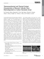
Figures 1 and 2 compare field emission scanning elec-
tron microscopy ͑FESEM͒ cross-sectional images of the
nanowire array/PAA composite and nanowire array/SU-8
composite. The image of the nanowire/SU-8 composite re-
veals that the nanowires are completely embedded in the
polymer matrix with crystallographic cleavage planes evi-
dent in the Bi
2
Te
3
. A higher magnification image of the com-
posite cross section clearly shows that the fracture proceeded
by crack propagation through the nanowire, and not through
the interface of the nanowire and SU-8 matrix, suggesting
that the nanowire /SU-8 interface is of high structural integ-
rity. On the other hand, the FESEM image obtained from the
nanowire array/PAA composite shows that the fracture
propagates preferentially along the interface between the
nanowire and PAA. The crystallographic cleavage planes ob-
served in the fractured nanowire array/SU-8 composites can
be attributed to the weak van der Waals bonding between the
Te–Te atomic planes in Bi
2
Te
3
crystal structure,
25,26
which is
preferentially oriented in the nanowire arrays such that the
c-axis of the pseudohexagonal unit cell is perpendicular to
the nanowire axis.
A photoacoustic ͑PA͒ technique was used to measure the
thermal conductivity of the nanowire array composites. A
modulated laser was used to heat the surface of the sample,
which was surrounded by a sealed acoustic chamber filled
with He gas. The sample and a quartz reference were coated
with a thin metal film ͑Ti with a thickness of approximately
80 nm͒ to absorb the laser energy. The laser was a continu-
ous power fiber laser ͑1064 nm͒ and an acoustic-optical
chopper was used to modulate the beam in the 1–10 kHz
range. A microphone mounted in the side wall of the acoustic
chamber was used to measure the amplitude and phase shift
of the pressure signal. The measured acoustic response was
related to thermal properties of the sample using a one-
dimensional heat conduction model.
27
Details of the PA mea-
surement technique are provided elsewhere.
27–29
The 300 K thermal conductivity values obtained by the
PA technique were 1.4Ϯ0.07 W / m K for the Bi
2
Te
3
nano-
wire array/PAA composite and 1.1Ϯ0.06 W / m K for
Bi
2
Te
3
nanowire array/SU-8 composite. The thermal conduc-
tivity of the PAA matrix alone ͑i.e., PAA/air composite͒ was
measured as 0.38Ϯ0.02 W / m K. Assuming that the volume
fraction of the nanowire material is f
nw
, and that the compos-
ite is dense such that the volume fraction of the matrix is
1−f
nw
, the thermal conductivity of the Bi
2
Te
3
nanowire ar-
ray composite can be estimated as f
nw
nw
+͑1−f
nw
͒
m
,
where
nw
and
m
are the thermal conductivities of the
nanowire and the matrix, respectively. Taking into account
that the porosity fraction in the PAA template was
TABLE I. SU-8 processing steps and optimized baking time for nanowire array infiltration.
SU-8 2005
viscosity
͑cst͒
Layer
thickness
͑
m͒
Soft bake
at 65 ° C
͑min͒
Soft bake
at 95 ° C
͑min͒
Post exposure bake
at 65 ° C
͑min͒
Post exposure bake
at 95 ° C
͑min͒
Hard bake at
150 ° C
͑min͒
45 40 2 30 1 10 30
FIG. 1. ͑a͒ FESEM image showing the pristine fractured cross section of an
as-grown Bi
2
Te
3
nanowire array/PAA composite. ͑b͒ A magnified view of
the composite cross section that shows that the crack through the interface
between the PAA and the nanowire rather than through the nanowire, in
contrast to the observed behavior of cracks in the nanowire/SU-8 composite
͓Figs. 2͑a͒ and 2͑b͔͒.
223116-2 Biswas et al. Appl. Phys. Lett. 94, 223116 ͑2009͒
Downloaded 29 Jun 2009 to 128.46.220.88. Redistribution subject to AIP license or copyright; see />0.72Ϯ0.025, the effective PAA thermal conductivity is
1.31Ϯ0.1 W / m K. This value can be used to estimate the
contribution from the Bi
2
Te
3
nanowires in the composite,
which is calculated to be 1.44Ϯ 0.1 W/ m K. In the second
case, the thermal conductivity of the Bi
2
Te
3
nanowire array/
SU-8 composite was measured to be 1.1Ϯ 0.06 W/ m K. Us-
ing the volume fraction and thermal conductivity of SU-8 as
0.28Ϯ0.025 and 0.2 W/m K, respectively, the effective ther-
mal conductivity of the Bi
2
Te
3
nanowires in the composite is
1.45Ϯ0.09 W / m K. The thermal conductivity values ob-
tained for Bi
2
Te
3
nanowires lie within the range of experi-
mental error and in conformation with previously reported
data.
5
In conclusion, we have demonstrated a method for over-
coming a significant obstacle to utilizing nanowire arrays as
thermoelectric materials. The dense ͑72% nanowire volume
fraction͒ and mechanically robust nanowire array/SU-8 com-
posites fabricated by replacing the PAA template substan-
tially reduce the matrix thermal shunt. Thermal conductivity
measurements by the PA technique reflect a 21% reduction in
the composite’s thermal conductivity when the PAA matrix
͑
=1.31 W / mK͒ is replaced with SU-8 epoxy resin ͑
=0.2 W / mK͒. This study with relatively large diameter,
nonalloyed Bi
2
Te
3
nanowires represents a baseline for the
improvements that might be expected from replacing PAA
with SU-8. For example, replacement of PAA with SU-8 in a
composite with f
nw
=0.7 and smaller diameter alloyed nano-
wires with an effective thermal conductivity of 1 W/m K
would reduce the composite thermal conductivity from 1.09
to 0.76 W/m K, thereby increasing the ZT of the composite
by 44%.
This work was supported by a grant from the Office of
Naval Research ͑Grant No. N000140610641͒.
1
Y. Ma, Q. Hao, B. Poudel, Y. Lan, B. Yu, D. Wang, G. Chen, and Z. Ren,
Nano Lett. 8, 2580 ͑2008͒.
2
B. Poudel, Q. Hao, Y. Ma, Y. C. Lan, A. Minnich, B. Yu, X. Yan, D. Z.
Wang, A. V. Muto, D. Vashaee, X. Y. Chen, J. M. Liu, M. S. Dresselhaus,
G. Chen, and Z. F. Ren, Science 320, 634 ͑2008͒.
3
R. Venkatasubramanian, E. Siivola, T. Colpitts, and B. O’Quinn, Nature
͑London͒ 413, 597 ͑2001͒.
4
S. A. Sapp, B. B. Lakshmi, and C. R. Martin, Adv. Mater. ͑Weinheim,
Ger.͒ 11, 402 ͑1999͒.
5
D A. Borca-Tasciuc, G. Chen, A. Prieto, M. S. Martín-González, A.
Stacy, T. Sands, M. A. Ryan, and J. P. Fleurial, Appl. Phys. Lett. 85, 6001
͑2004͒.
6
C. G. Jin, X. Q. Xiang, C. Jia, W. F. Liu, W. L. Cai, L. Z. Yao, and X. G.
Li, J. Phys. Chem. B 108, 1844 ͑2004͒.
7
M. S. Sander, A. L. Prieto, R. Gronsky, T. Sands, and A. M. Stacy, Adv.
Mater. ͑Weinheim, Ger.͒ 14, 665 ͑2002͒.
8
M. S. Sander, R. Gronsky, T. Sands, and A. M. Stacy, Chem. Mater. 15,
335 ͑2003͒.
9
W. Wang, Q. Huang, F. Jia, and J. Zhu, J. Appl. Phys. 96,615͑2004͒.
10
H. Masuda, H. Yamada, M. Satoh, H. Asoh, M. Nakao, and T. Tamamura,
Appl. Phys. Lett. 71, 2770 ͑1997͒.
11
O. Jessensky, F. Muller, and U. Gosele, Appl. Phys. Lett. 72,1173͑1998͒.
12
W. Lee, R. Ji, U. Gosele, and K. Nielsch, Nature Mater. 5,741͑2006͒.
13
H. Masuda, K. Yada, and A. Osaka, Jpn. J. Appl. Phys., Part 2 37, L1340
͑1998͒.
14
K. Nielsch, Nano Lett. 2, 677 ͑2002͒.
15
D. A. Borca-Tasciuc and G. Chen, J. Appl. Phys. 97, 084303 ͑2005͒.
16
J. H. Zhou, C. G. Jin, J. H. Seol, X. G. Li, and L. Shi, Appl. Phys. Lett.
87, 133109 ͑2005͒.
17
A. R. Abramson, W. C. Kim, S. T. Huxtable, H. Yan, Y. Wu, A. Majum-
dar, C L. Tien, and P. Yang, J. Microelectromech. Syst. 13,505͑2004͒.
18
J. R. Lim, J. F. Whitacre, J. P. Fleurial, C. K. Huang, M. A. Ryan, and N.
V. Myung, Adv. Mater. ͑Weinheim, Ger.͒ 17, 1488 ͑2005͒.
19
A. D. Campo and C. Greiner, J. Micromech. Microeng. 17,R81͑2007͒.
20
E. H. Conradie and D. F. Moore, J. Micromech. Microeng. 12,368
͑2002͒.
21
MicroChem ͑ />22
K. Biswas, V. Rawat, M. DaSilva, and T. Sands, 2nd Energy Nanotech-
nology International Conference, ASME, 2007 ͑unpublished͒,p.45029.
23
K. Biswas, Y. Qin, M. DaSilva, R. Reifenberger, and T. Sands, Phys.
Status Solidi A 204, 3152 ͑2007͒.
24
R. L. Barber, M. K. Ghantasala, R. Divan, K. D. Vora, E. C. Harvey, and
D. C. Mancini, Microsyst. Technol. 11, 303 ͑2005͒.
25
G. E. Shoemake, J. A. Rayne, and J. R. W. Ure, Phys. Rev. 185,1046
͑1969͒.
26
M. H. Francombe, Br. J. Appl. Phys. 9, 415 ͑1958͒.
27
H. Hu, X. Wang, and X. C. Xu, J. Appl. Phys. 86, 3953 ͑1999͒.
28
X. Wang, H. Hu, and X. Xu, ASME J. Heat Transfer 123,138͑2001͒.
29
B. A. Cola, R. Karru, C. Cheng, X. Xu, and T. S. Fisher, IEEE Trans.
Compon. Packag. Technol. 31,46͑2008͒.
FIG. 2. ͑a͒ FESEM image showing the pristine fractured cross section of a
Bi
2
Te
3
nanowire array/SU-8 composite. The nanowires are embedded in the
SU-8 epoxy matrix confirming complete infiltration of the epoxy. ͑b͒ A
magnified view of the composite cross-section that shows that the fracture
plane propagates through the nanowire—exposing crystallographic cleavage
planes in Bi
2
Te
3
—and not through the interface between the nanowire and
the SU-8 epoxy.
223116-3 Biswas et al. Appl. Phys. Lett. 94, 223116 ͑2009͒
Downloaded 29 Jun 2009 to 128.46.220.88. Redistribution subject to AIP license or copyright; see />