Power Quality Harmonics Analysis and Real Measurements Data Part 7 pdf
Bạn đang xem bản rút gọn của tài liệu. Xem và tải ngay bản đầy đủ của tài liệu tại đây (1.59 MB, 20 trang )
Part 2
Converters
4
Study of LCC Resonant Transistor DC / DC
Converter with Capacitive Output Filter
Nikolay Bankov, Aleksandar Vuchev and Georgi Terziyski
University of Food Technologies – Plovdiv
Bulgaria
1. Introduction
The transistor LCC resonant DC/DC converters of electrical energy, working at frequencies
higher than the resonant one, have found application in building powerful energy supplying
equipment for various electrical technologies (Cheron et al., 1985; Malesani et al., 1995; Jyothi
& Jaison, 2009). To a great extent, this is due to their remarkable power and mass-dimension
parameters, as well as, to their high operating reliability. Besides, in a very wide-working field,
the LCC resonant converters behave like current sources with big internal impedance. These
converters are entirely fit for work in the whole range from no-load to short circuit while
retaining the conditions for soft commutation of the controllable switches.
There is a multitude of publications, dedicated to the theoretical investigation of the LCC
resonant converters working at a frequency higher than their resonant one (Malesani et al.,
1995; Ivensky et al. 1999). In their studies most often the first harmonic analysis is used,
which is practically precise enough only in the field of high loads of the converter. With the
decrease in the load the mistakes related to using the method of the first harmonic could
obtain fairly considerable values.
During the analysis, the influence of the auxiliary (snubber) capacitors on the controllable
switches is usually neglected, and in case of availability of a matching transformer, only its
transformation ratio is taken into account. Thus, a very precise description of the converter
operation in a wide range of load changes is achieved. However, when the load resistance
has a considerable value, the models created following the method mentioned above are not
correct. They cannot be used to explain what the permissible limitations of load change
depend on in case of retaining the conditions for soft commutation at zero voltage of the
controllable switches – zero voltage switching (ZVS).
The aim of the present work is the study of a transistor LCC resonant DC/DC converter of
electrical energy, working at frequencies higher than the resonant one. The possible operation
modes of the converter with accounting the influence of the damping capacitors and the
parameters of the matching transformer are of interest as well. Building the output
characteristics based on the results from a state plane analysis and suggesting a methodology
for designing, the converter is to be done. Drawing the boundary curves between the different
operating modes of the converter in the plane of the output characteristics, as well as outlining
the area of natural commutation of the controllable switches are also among the aims of this
work. Last but not least, the work aims at designing and experimental investigating a
laboratory prototype of the LCC resonant converter under consideration.
Power Quality Harmonics Analysis and Real Measurements Data
112
2. Modes of operation of the converter
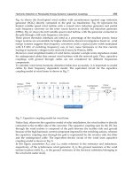
The circuit diagram of the LCC transistor resonant DC/DC converter under investigation is
shown in figure 1. It consists of an inverter (controllable switches constructed on base of the
transistors Q
1
÷Q
4
with freewheeling diodes D
1
÷D
4
), a resonant circuit (L, С), a matching
transformer Tr, an uncontrollable rectifier (D
5
÷D
8
), capacitive input and output filters (C
F1
и
C
F2
) and a load resistor (R
0
). The snubber capacitors (C
1
÷C
4
) are connected with the
transistors in parallel.
The output power of the converter is controlled by changing the operating frequency, which
is higher than the resonant frequency of the resonant circuit.
It is assumed that all the elements in the converter circuit (except for the matching
transformer) are ideal, and the pulsations of the input and output voltages can be neglected.
Fig. 1. Circuit diagram of the LCC transistor DC/DC converter
All snubber capacitors C
1
÷C
4
are equivalent in practice to just a single capacitor C
S
(dotted
line in fig.1), connected in parallel to the output of the inverter. The capacity of the capacitor
C
S
is equal to the capacity of each of the snubber capacitors C
1
÷C
4
.
The matching transformer Tr is shown in fig.1 together with its simplified equivalent circuit
under the condition that the magnetizing current of the transformer is negligible with
respect to the current in the resonant circuit. Then this transformer comprises both the full
leakage inductance L
S
and the natural capacity of the windings С
0
, reduced to the primary
winding, as well as an ideal transformer with its transformation ratio equal to k.
The leakage inductance L
S
is connected in series with the inductance of the resonant circuit L
and can be regarded as part of it
.
The natural capacity C
0
takes into account the capacity
between the windings and the different layers in each winding of the matching transformer.
C
0
can has an essential value, especially with stepping up transformers (Liu et al., 2009).
Together with the capacity С
0
the resonant circuit becomes a circuit of the third order (L, C
and С
0
), while the converter could be regarded as LCC resonant DC/DC converter with a
capacitive output filter.
The parasitic parameters of the matching transformer – leakage inductance and natural
capacity of the windings – should be taken into account only at high voltages and high
operating frequencies of the converter. At voltages lower than 1000 V and frequencies lower
Study of LCC Resonant Transistor DC / DC Converter with Capacitive Output Filter
113
than 100 kHz they can be neglected, and the capacitor С
0
should be placed additionally (Liu
et al., 2009).
Because of the availability of the capacitor C
S
, the commutations in the output voltage of the
inverter (u
a
) are not instantaneous. They start with switching off the transistors Q
1
/Q
3
or
Q
2
/Q
4
and end up when the equivalent snubber capacitor is recharged from +U
d
to –U
d
or
backwards and the freewheeling diodes D
2
/D
4
or D
1
/D
3
start conducting. In practice the
capacitors С
2
and С
4
discharge from +U
d
to 0, while С
1
and С
3
recharge from 0 to+U
d
or
backwards. During these commutations, any of the transistors and freewheeling diodes of
the inverter does not conduct and the current flowed through the resonant circuit is closed
through the capacitor С
S
.
Because of the availability of the capacitor C
0
, the commutations in the input voltage of the
rectifier (u
b
) are not instantaneous either. They start when the diode pairs (D
5
/D
7
or D
6
/D
8
)
stop conducting at the moments of setting the current to zero through the resonant circuit
and end up with the other diode pair (D
6
/D
8
или D
5
/D
7
) start conducting, when the
capacitor С
0
recharges from +kU
0
to –kU
0
or backwards. During these commutations, any of
the diodes of the rectifier does not conduct and the current flowed through the resonant
circuit is closed through the capacitor С
0
.
The condition for natural switching on of the controllable switches at zero voltage (ZVS) is
fulfilled if the equivalent snubber capacitor С
S
always manages to recharge from +U
d
to –U
d
or backwards. At modes, close to no-load, the recharging of С
S
is possible due to the
availability of the capacitor C
0
. It ensures the flow of current through the resonant circuit,
even when the diodes of the rectifier do not conduct.
When the load and the operating frequency are deeply changed, three different operation
modes of the converter can be observed.
It is characteristic for the first mode that the commutations in the rectifier occur entirely in
the intervals for conducting of the transistors in the inverter. This mode is the main operation
mode of the converter. It is observed at comparatively small values of the load resistor R
0
.
At the second mode the commutation in the rectifier ends during the commutation in the
inverter, i.e., the rectifier diodes start conducting when both the transistors and the
freewheeling diodes of the inverter are closed. This is the medial operation mode and it is only
observed in a narrow zone, defined by the change of the load resistor value which is
however not immediate to no-load.
At modes, which are very close to no-load the third case is observed. The commutations in
the rectifier now complete after the ones in the inverter, i.e. the rectifier diodes start
conducting after the conduction beginning of the corresponding inverter’s freewheeling
diodes. This mode is the boundary operation mode with respect to no-load.
3. Analysis of the converter
In order to obtain general results, it is necessary to normalize all quantities characterizing
the converter’s state. The following quantities are included into relative units:
CCd
xU uU
′
== - Voltage of the capacitor С;
0d
i
yI
UZ
′
== - Current in the resonant circuit;
d
UkUU
00
=
′
- Output voltage;
Power Quality Harmonics Analysis and Real Measurements Data
114
0
0
0
ZU
kI
I
d
=
′
- Output current;
dCmCm
UUU =
′
- Maximum voltage of the capacitor С;
0
ωων =
- Distraction of the resonant circuit,
where
ω is the operating frequency and
LC1ω
0
=
and
0
ZLC=
are the resonant
frequency and the characteristic impedance of the resonant circuit L-C correspondingly.
3.1 Analysis at the main operation mode of the converter
Considering the influence of the capacitors С
S
and С
0
, the main operation mode of the
converter can be divided into eight consecutive intervals, whose equivalent circuits are
shown in fig. 2. By the trajectory of the depicting point in the state plane
()
;
C
xU
y
I
′′
==,
shown in fig. 3, the converter’s work is also illustrated, as well as by the waveform diagrams
in fig.4.
The following four centers of circle arcs, constituting the trajectory of the depicting point,
correspond to the respective intervals of conduction by the transistors and freewheeling
diodes in the inverter: interval 1: Q
1
/Q
3
-
()
0
1;0U
′
− ; interval 3: D
2
/D
4
-
()
0
1;0U
′
−− ;
interval 5: Q
2
/Q
4
-
()
0
1;0U
′
−+ ; interval 7: D
1
/D
3
-
()
0
1;0U
′
+ .
The intervals 2 and 6 correspond to the commutations in the inverter. The capacitors С and
С
S
then are connected in series and the sinusoidal quantities have angular frequency of
10
1ω
E
LC=
′
where
()
1ES S
CCCCC=+. For the time intervals 2 and 6 the input current i
d
is equal to zero. These pauses in the form of the input current i
d
(fig. 4) are the cause for
increasing the maximum current value through the transistors but they do not influence the
form of the output characteristics of the converter.
Fig. 2. Equivalent circuits at the main operation mode of the converter.
The intervals 4 and 8 correspond to the commutations in the rectifier. The capacitors С and
С
0
are then connected in series and the sinusoidal quantities have angular frequency of
20
1ω
E
LC=
′′
where
()
20 0E
CCCCC=+. For the time intervals 4 and 8, the output current
i
0
is equal to zero. Pauses occur in the form of the output current i
0
, decreasing its average
value by
0
ΔI (fig. 4) and essentially influence the form of the output characteristics of the
converter.
Study of LCC Resonant Transistor DC / DC Converter with Capacitive Output Filter
115
Fig. 3. Trajectory of the depicting point at the main mode of the converter operation.
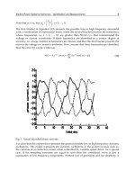
Fig. 4. Waveforms of the voltages and currents at the main operation mode of the converter
Power Quality Harmonics Analysis and Real Measurements Data
116
It has been proved in (Cheron, 1989; Bankov, 2009) that in the state plane (fig. 3) the points,
corresponding to the beginning (p.М
2
) and the end (p.М
3
) of the commutation in the inverter
belong to the same arc with its centre in point
()
0
;0U
′
− . It can be proved the same way that the
points, corresponding to the beginning (p.М
8
) and the end (p.М
1
) of the commutation in the
rectifier belong to an arc with its centre in point
()
1;0 . It is important to note that only the end
points are of importance on these arcs. The central angles of these arcs do not matter either,
because as during the commutations in the inverter and rectifier the electric quantities change
correspondingly with angular frequencies
0
ω
′
and
0
ω
′′
, not with
0
ω .
The following designations are made:
1 S
aCC=
()
11 1
1na a=+ (1)
20
aCC=
()
22 2
1na a=+ (2)
312
11 1naa=+ + (3)
For the state plane shown in fig, 3 the following dependencies are valid:
()()
22
22
101202
11xU
y
xU
y
′′
−+ + = −+ + (4)
() ()
22
22
20 2 30 3
xU
y
xU
y
′′
++=++ (5)
()()
22
22
303404
11xU
y
xU
y
′′
++ + = ++ + (6)
()
()
2
2
22
4455
11x
y
x
y
++=++ (7)
From the existing symmetry with respect to the origin of the coordinate system of the state
plane it follows:
51
xx=− (8)
51
y
y=−
(9)
During the commutations in the inverter and rectifier, the voltages of the capacitors С
S
and
С
0
change correspondingly by the values 2
d
U and
0
2kU , and the voltage of the
commutating capacitor C changes respectively by the values
1
2
d
aU
and
20
2akU
.
Consequently:
32 1
2xx a=+
(10)
54 20
2xx aU
′
=−
(11)
The equations (4)÷(11) allow for calculating the coordinates of the points М
1
÷М
4
in the state
plane, which are the starting values of the current through the inductor L and the voltage of
Study of LCC Resonant Transistor DC / DC Converter with Capacitive Output Filter
117
the commutating capacitor C in relative units for each interval of converter operation. The
expressions for the coordinates are in function of
0
U
′
,
Cm
U
′
,
1
a and
2
a :
120
2
Cm
xU aU
′′
=− + (12)
()
120 20
41
Cm
yaUUaU
′′ ′
=−+ (13)
2
20 201
Cm
xUU aU a
′′ ′
=−− (14)
()
()
()
2
20 0 20 1
2
22002010
20 20
2
222
41
Cm Cm
Cm Cm
Cm
UaUUUaUa
y U aU UU aU a U
aU U aU
′′′′′
−+ − + +⋅
′′′′′ ′
=⋅− + + − − + − +
′′ ′
+−+
(15)
2
30 201Cm
xUU aU a
′′ ′
=−+ (16)
()
()
2
0201
3
2
02010
22
Cm Cm
Cm Cm
UUUaUa
y
UUUaUaU
′′′ ′
−+−⋅
=
′′′ ′ ′
⋅+ − +++
(17)
4 Cm
xU
′
= (18)
4
0y =
(19)
For converters with only two reactive elements (L and C) in the resonant circuit the
expression for its output current
0
I
′
is known from (Al Haddad et al., 1986; Cheron, 1989):
01
2
Cm
IU
ν
π
′′
=
(20)
The LCC converter under consideration has three reactive elements in its resonant circuit (L,
С и C
0
). From fig.4 it can be seen that its output current
0
I
′
decreases by the value
020
2IaU
ν
π
′′
Δ=
:
()
0020
22
Cm Cm
IU I UaU
ν
πν π
′′ ′ ′ ′
=−Δ=− (21)
The following equation is known:
()
01 2 3 4
tttt
π
ω
ν
=+++
, (22)
where the times
t
1
÷t
4
represent the durations of the different stages – from 1 to 4.
For the times of the four intervals at the main mode of operation of the converter within a
half-cycle the following equations hold:
21
1
020 10
1
11
yy
tarctg arctg
xU xU
ω
=−
′′
−+− −+−
(23a)
Power Quality Harmonics Analysis and Real Measurements Data
118
at
20
1xU
′
≤− and
10
1xU
′
≤−
21
1
02010
1
11
yy
tarctg arctg
xU xU
π
ω
=− −
′′
−+ − +−
(23b)
at
20
1xU
′
≥− and
10
1xU
′
≤−
21
1
02010
1
11
yy
tarctg arctg
xU xU
ω
=+
′′
−+− −+
(23c)
at
20
1xU
′
≥− and
10
1xU
′
≥−
12 13
2
10 2 0 3 0
1
11
ny ny
tarctg arctg
nxUxU
ω
=−
′′
−+ ++
(24a)
at
20
1xU
′
≥−
12 13
2
10 2 0 3 0
1
11
ny ny
tarctg arctg
nxUxU
ω
=−
′′
−+ ++
(24b)
at
20
1xU
′
≤−
3
3
03 0
1
1
y
tarctg
xU
ω
=
′
++
(25)
21
4
20 1 0
1
1
ny
tarctg
nxU
ω
=
′
−+−
(26a)
at
10
1xU
′
≤−
21
4
20 1 0
1
1
ny
tarctg
nxU
π
ω
=−
′
−+
(26b)
at
10
1xU
′
≥−
It should be taken into consideration that for stages 1 and 3 the electric quantities change
with angular frequency
0
ω
, while for stages 2 and 4 – the angular frequencies are
respectively
010
ωωn
′
= and
020
ωωn
′′
= .
3.2 Analysis at the boundary operation mode of the converter
At this mode, the operation of the converter for a cycle can be divided into eight consecutive
stages (intervals), whose equivalent circuits are shown in fig. 5. It makes impression that the
sinusoidal quantities in the different equivalent circuits have three different angular
frequencies:
Study of LCC Resonant Transistor DC / DC Converter with Capacitive Output Filter
119
LC1ω
0
=
for stages 4 and 8;
20
1ω
E
LC=
′′
, where
()
20 0E
CCCCC=+
, for stages 1, 3, 5 and 7;
30
1ω
E
LC=
′′′
, where
()
30 00ES S S
C CC C CC CC C C=++
, for stages 2 and 6.
Fig. 5. Equivalent circuits at the boundary operation mode of the converter
In this case the representation in the state plane becomes complex and requires the use of
two state planes (fig.6). One of them is
()
;
C
xU
y
I
′′
==
and it is used for presenting stages 4
and 8, the other is
()
00
;xy , where:
2
0
E
Cd
xu U=
;
0
2
dE
i
y
ULC
=
.
Fig. 6. Trajectory of the depicting point at the boundary mode of operation of the converter
Power Quality Harmonics Analysis and Real Measurements Data
120
Stages 2 and 6 correspond to the commutations in the inverter.
The commutations in the rectifier begin in p.
0
1
M
or p.
0
5
M
and end in p.
0
4
M
or p.
0
8
M
,
comprising stages 1,2 and 3 or 5,6 and 7.
The transistors conduct for the time of stages 1 and 5, the freewheeling diodes – for the time
of stages 3, 4, 7 and 8, and the rectifier diodes – for the time of stages 4 and 8.
The following equations are obtained in correspondence with the trajectory of the depicting
point for this mode of operation (fig.6):
()()()
222
000
122
11xxy−=−+ (27)
() () () ()
2222
0000
2233
xyxy+=+ (28)
()()()()
22 22
0000
3344
11xyxy++ =++ (29)
()
()
()
2
22
404 01
11xU
y
Ux
′′
++ + = + − (30)
During the commutations in the inverter, the voltage of the capacitor С
Е2
changes by the
value
2
2
dS E
UC C and consequently:
00 2
32 12
2xx an=+ (31)
The same way during the commutation in the rectifier, the voltage of the capacitor С
Е2
changes by the value
00 2
2
E
kU C C and consequently:
()
00
41 0 2
21xx U a
′
=+ +
(32)
From the principle of continuity of the current through the inductor L and of the voltage in
the capacitor C it follows:
0
44 0
xxU
′
=+ (33)
0
424
y
n
y
=
(34)
where
()
;
ii
x
y
and
()
00
;
ii
xy are the coordinates of
i
M
and
0
i
M
respectively.
The equations (27)÷(34) allow for defining the coordinates of the points
0
1
M
÷
0
4
M
in the
state plane:
0
10
Cm
xUU
′′
=− − (35)
0
1
0y =
(36)
()( )
20 0 20
02
212
2
1
Cm
UaU UaU
xan
a
′′′′
−++
=−
(37)
Study of LCC Resonant Transistor DC / DC Converter with Capacitive Output Filter
121
()
()
2
2
00
22
11
Cm o
yU U x
′′
=++−− (38)
()( )
20 0 20
02
312
2
1
Cm
UaU UaU
xan
a
′′′′
−++
=+
(39)
() () ()
222
00 00
32 2 3
yx y x=+−
(40)
()
0
402
12
Cm
xUU a
′′
=− + +
(41)
()()
0
420020
21
Cm
yaUUaUU
′′′′
=++ −
(42)
At the boundary operation mode the output current
0
I
′
is defined by expression (21) again,
where t
1
÷t
4
represent the times of the different stages – from 1 to 4.
For the times of the four intervals at the boundary operation mode of the converter within a
half-cycle the following equations hold:
0
2
1
0
20
2
1
1
y
tarctg
n
x
ω
=
−
at
0
2
1x ≤ (43a)
0
2
1
0
20
2
1
1
y
tarctg
n
x
π
ω
=−
−
at
0
2
1x ≥
(43b)
() ()
00
32 33
2
00
30
22 23
1
11
ny ny
tarctgarctg
n
nx nx
π
ω
=− −
−+
at
0
2
1x ≤ (44a)
() ()
00
32 33
2
00
30
22 2 3
1
11
ny ny
tarctg arctg
n
nx n x
ω
=−
−+
at
0
2
1x ≥ (44b)
00
34
3
00
20
34
1
11
yy
tarctgarctg
n
xx
ω
=−
++
(45)
4
4
040
1
1
y
tarctg
xU
ω
=
′
++
(46)
It should be taken into consideration that for stages 1 and 3 the electric quantities change by
angular frequency
020
n
ωω
′′
=
, while for stages 2 and 4 the angular frequencies are
correspondingly
030
n
ωω
′′′
=
and
0
ω
.
Power Quality Harmonics Analysis and Real Measurements Data
122
4. Output characteristics and boundary curves
On the basis of the analysis results, equations for the output characteristics are obtained
individually for both the main and the boundary modes of the converter operation. Besides,
expressions for the boundary curves of the separate modes are also derived.
4.1 Output characteristics and boundary curves at the main operation mode
From equation (21)
Cm
U
′
is expressed in function of
0
U
′
,
0
I
′
,
ν
and
2
a
020
2
Cm
UIaU
π
ν
′′′
=+
(47)
By means of expression (47)
Cm
U
′
is eliminated from the equations (12)÷(18). After
consecutive substitution of expressions (12)÷(18) in equations (23)÷(26) as well as of
expressions (23)÷(26) in equation (22), an expression of the kind
()
0012
,, ,UfI aa
ν
′′
=
is
obtained. Its solution provides with the possibility to build the output characteristics of the
converter in relative units at the main mode of operation and at regulation by means of
changing the operating frequency. The output characteristics of the converter respectively
for ν=1.2; 1.3; 1.4; 1.5; 1.8; 2.5; 3.0; 3.3165; 3,6 and а
1
=0.1; а
2
=0.2 as well as for ν=1.2; 1.3; 1.4;
1.5; 1.6; 1.8 and а
1
=0.1; а
2
=1.0 are shown in fig.7-a and 7-b.
The comparison of these characteristics to the known ones from (Al Haddad et al., 1986;
Cheron, 1989) shows the entire influence of the capacitors С
S
и С
0
. It can be seen that the
output characteristics become more vertical and the converter can be regarded to a great
extent as a source of current, stable at operation even at short circuit. Besides, an area of
operation is noticeable, in which
0
1U
′
>
.
At the main operation mode the commutations in the rectifier (stages 4 and 8) must always
end before the commutations in the inverter have started. This is guaranteed if the following
condition is fulfilled:
12
xx≤
(48)
In order to enable natural switching of the controllable switches at zero voltage (ZVS), the
commutations in the inverter (stages 2 and 6) should always end before the current in the
resonant circuit becomes zero. This is guaranteed if the following condition is fulfilled:
3 Cm
xU
′
≤
(49)
If the condition (49) is not fulfilled, then switching a pair of controllable switches off does
not lead to natural switching the other pair of controllable switches on at zero voltage and
then the converter stops working. It should be emphasized that these commutation mistakes
do not lead to emergency modes and they are not dangerous to the converter. When it
„misses“, all the semiconductor switches stop conducting and the converter just stops
working. This is one of the big advantages of the resonant converters working at frequencies
higher than the resonant one.
Study of LCC Resonant Transistor DC / DC Converter with Capacitive Output Filter
123
a)
b)
Fig. 7. Output characteristics of the LCC transistor DC/DC converter
Equations (12), (14) and (47) are substituted in condition (48), while equations (16) and (47)
are substituted in condition (49). Then the inequalities (48) and (49) obtain the form:
120
0
0
2
1
aaU
I
U
ν
π
′
+
′
≥⋅
′
+
(50)
120
0
0
2
1
aaU
I
U
ν
π
′
−
′
≥⋅
′
−
(51)
Inequalities (50) и (51) enable with the possibility to draw the boundary curve A between
the main and the medial modes of operation of the converter, as well as the border of the
natural commutation – curve L
3
(fig. 7-а) or curve L
4
(fig. 7-b) in the plane of the output
characteristics. It can be seen that the area of the main operation mode of the converter is
limited within the boundary curves А and L
3
or L
4
. The bigger the capacity of the capacitors
Power Quality Harmonics Analysis and Real Measurements Data
124
С
S
and С
0
, the smaller this area is. However, the increase of the snubber capacitors leads to a
decrease in the commutation losses in the transistors as well as to limiting the
electromagnetic interferences in the converter.
The expression (51) defines the borders, beyond which the converter stops working because
of the breakage in the conditions for natural switching the controllable switches on at zero
voltage (ZVS). Exemplary boundary curves have been drawn in the plane of the output
characteristics (fig.8) at а
1
=0.10. Four values have been chosen for the other parameter: а
2
=
0.05; 0.1; 0.2 and 1.0. When the capacity of the capacitor С
0
is smaller or equal to that of the
snubber capacitors C
S
()
12
aa≥ , then the converter is fit for work in the area between the
curve L
1
or L
2
and the x-axis (the abscissa). Only the main operation mode of the converter
is possible in this area. The increase in the load resistance or in the operating frequency
leads to stopping the operation of the converter before it has accomplished a transition
towards the medial and the boundary modes of work.
When C
0
has a higher value than the value of C
S
()
12
aa< then the boundary curve of the
area of converter operation with ZVS is displaced upward (curve L
3
or L
4
). It is possible now
to achieve even a no-load mode.
Fig. 8. Borders of the converter operation capability
4.2 Output characteristics and boundary curves at the boundary operation mode
Applying expression (47) for equations (35)÷(42)
Cm
U
′
is eliminated. After that, by a
consecutive substitution of expressions (35)÷(42) in equations (43)÷(45) as well as of
expressions (43)÷(46) in equation (22), a dependence of the kind
()
0012
,, ,U
f
Iaa
ν
′′
= is
obtained. Its solving enables with a possibility to build the outer (output) characteristics of
the converter in relative units at the boundary operation mode under consideration and at
regulation by changing the operating frequency. Such characteristics are shown in fig. 7-а
for ν = 3.0; 3.3165; 3.6 and а
1
=0.1; а
2
=0.2 and in fig. 7-b for ν =1.5; 1.6; 1.8 and а
1
=0.1; а
2
=1.0.
At the boundary operation mode, the diodes of the rectifier have to start conducting after
opening the freewheeling diodes of the inverter. This is guaranteed if the following
condition is fulfilled:
Study of LCC Resonant Transistor DC / DC Converter with Capacitive Output Filter
125
00
43
xx≥
(52)
After substitution of equations (39), (41) и (47) in the inequality (52), the mentioned above
condition obtains the form:
20 1
0
0
2
1
aU a
I
U
ν
π
′
−
′
≤⋅
′
+
(53)
Condition (53) gives the possibility to define the area of the boundary operation mode of the
converter in the plane of the output characteristics (fig. 7-а and fig. 7-b). It is limited between
the y-axis (the ordinate) and the boundary curve B. It can be seen that the converter stays
absolutely fit for work at high-Ohm loads, including at a no-load mode. It is due mainly to
the capacitor С
0
. With the increase in its capacity (increase of a
2
) the area of the boundary
operation mode can also be increased.
5. Medial operation mode of the converter
At this operation mode, the diodes of the rectifier start conducting during the commutation
in the inverter. The equivalent circuits, corresponding to this mode for a cycle, are shown in
fig.9. In this case, the sinusoidal quantities have four different angular frequencies:
LC1ω
0
= for stages 4 and 8;
10
1ω
E
LC=
′
, where
()
1ES S
CCCCC=+, for stages 3 and 7;
20
1ω
E
LC=
′′
, where
()
20 0E
CCCCC=+, for stages 1 and 5;
30
1ω
E
LC=
′′′
, where
()
30 00ES S S
C CC C CC CC C C=++
, for stages 2 and 6.
Fig. 9. Equivalent circuits at the medial operation mode of the converter
Therefore, the analysis of the medial operation mode is considerably more complex. The
area in the plane of the output characteristics, within which this mode appears, however, is
completely defined by the boundary curves A and B for the main and the boundary modes
respectively. Having in mind the monotonous character of the output characteristics for the
other two modes, their building for the mode under consideration is possible through linear
interpolation. It is shown in fig. 7-а for ν = 3.0; 3.3165 as well as in fig. 7-b for ν=1.5; 1.6; 1.8.
The larger area of this mode corresponds to the higher capacity of the snubber capacitors C
S
and the smaller capacity of the capacitor C
0
.
Power Quality Harmonics Analysis and Real Measurements Data
126
6. Methododlogy for designing the converter
During the process of designing the LCC resonant DC/DC converter under consideration,
the following parameters are usually predetermined: power in the load Р
0,
output voltage U
0
and operating frequency f. Very often, the value of the power supply voltage U
d
is
predefined and the desired output voltage is obtained by adding a matching transformer.
The design of the converter could be carried out in the following order:
1. Choice of the frequency distraction ν
For converters, operating at frequencies higher than the resonant one, the frequency
distraction is usually chosen in the interval ν =1.1÷1.3. It should be noted here that if a
higher value of ν is chosen, the exchange of reactive energy between the resonant circuit and
the energy source increases, i.e., the current load on the elements in the circuit increases
while the stability of the output characteristics decreases. It is due to the increase in the
impedance of the resonant circuit of the converter.
2. Choice of the parameter
20
aCC=
The choice of this parameter is a compromise to a great extent. On the one hand, to avoid
the considerable change of the operating frequency during the operation of the converter
from nominal load to no-load mode, the capacitor С
0
(respectively the parameter а
2
) should
be big enough. On the other hand, with the increase of С
0
the current in the resonant circuit
increases and the efficiency of the converter decreases. It should be noted that a significant
increase in the current load on the elements in the scheme occurs at
2
1a > (Malesani et al.,
1995).
3. Choice of the parameter
1 S
aCC=
The parameter а
1
is usually chosen in the interval а
1
= 0.02÷0.20. The higher the value of а
1
(the bigger the capacity of the damping capacitors), the smaller the area of natural
commutation of the transistors in the plane of the output characteristics is. However, the
increase in the capacity of the snubber capacitors leads to a decrease in the commutation
losses and limitation of the electromagnetic interferences in the converter.
4. Choice of the coordinates of a nominal operating point
The values of the parameters а
1
and а
2
fully define the form of the output characteristics of
the converter. The nominal operating point with coordinates
0
I
′
and
0
U
′
lies on the
characteristic, corresponding to the chosen frequency distraction ν. It is desirable that this
point is close to the boundary of natural commutation so that the inverter could operate at a
high power factor (minimal exchange of reactive energy). If the converter operates with
sharp changes in the load and control frequency, however, it is then preferable to choose the
operating point in an area, relatively distant from the border of natural commutation. Thus,
automatic switching the converter off is avoided – a function, integrated in the control
drivers of power transistors.
5. Defining the transformation ratio of the matching transformer
The transformation ratio is defined, so that the required output voltage of the converter at
minimal power supply voltage and at maximum load is guaranteed:
Study of LCC Resonant Transistor DC / DC Converter with Capacitive Output Filter
127
0min
0
d
UU
k
U
′
⋅
≥ , (54)
where U
d min
is the minimal permissible value of the input voltage U
d
.
6. Calculating the parameters of the resonant circuit
The values of the elements in the resonant circuit L and C are defined by the expressions
related to the frequency distraction and the output current in relative units:
LCfπ2ωων
0
==
;
CLUU
kP
CLU
kI
I
dd 0
00
0
==
′
(55)
Solving the upper system of equations, it is obtained:
00
0
2
d
kUUI
L
fP
ν
π
′
= ;
0
00
2
d
P
C
f
kU U I
ν
π
=
′
(56)
7. Experimental investigations
For the purposes of the investigation, a laboratory prototype of the LCC resonant converter
under consideration was designed and made without a matching transformer and with the
following parameters: power supply voltage
500
d
U = V; output power
0
2.6P = кW,
output voltage
0
500U = V; operating frequency and frequency distraction at nominal load
50f = kHz and ν 1.3= ;
1
0.035a = ;
2
1a = ; coordinates of the nominal operating point -
0
1.43I
′
= and
0
1U
′
= . The following values of the elements in the resonant circuit were
obtained with the above parameters: 570L = μH;
0
30CC== nF. The controllable switches
of the inverter were IGBT transistors with built-in backward diodes of the type
IRG4PH40UD, while the diodes of the rectifier were of the type BYT12PI. Snubber capacitors
С
1
÷С
4
with capacity of 1 nF were connected in parallel to the transistors. Each transistor
possessed an individual driver control circuit. This driver supplied control voltage to the
gate of the corresponding transistor, if there was a control signal at the input of the
individual driver circuit and if the collector-emitter voltage of the transistor was practically
zero (ZVC commutation).
Experimental investigation was carried out during converter operation at frequencies
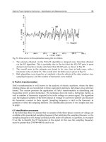
50f = kHz ( ν 1.3= ) and 61.54f = kHz ( ν 1.6= ). The dotted curve in fig.10 shows the
theoretical output characteristics, while the continuous curve shows the output
characteristics, obtained in result of the experiments.
A good match between the theoretical results and the ones from the experimental
investigation can be noted. The small differences between them are mostly due to the losses
in the semiconductor switches in their open state and the active losses in the elements of the
resonant circuit.
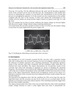
Oscillograms, illustrating respectively the main and the boundary operation modes of the
converter are shown in fig. 11 and fig. 12. These modes are obtained at a stable operating
frequency
61.54f = kHz ( ν 1.6= ) and at certain change of the load resistor. In the
oscillograms the following quantities in various combinations are shown: output voltage (u
a
)
and output current (i) of the inverter, input voltage (u
b
) and output current (i
0
) of the rectifier.
Power Quality Harmonics Analysis and Real Measurements Data
128
Fig. 10. Experimental output characteristics of the converter.
a)
u
a
200 V/div; i 5 А/div;
х=5µs/div
b)
u
a
200V/div; u
b
200V/div;
х=5µs/div
c)
i
0
5А/div; u
b
200V/div;
х=5µs/div
Fig. 11. Oscillograms illustrating the main operation mode of the converter
a)
u
a
200V/div; i 5А/div;
х=5µs/div
b)
u
a
200V/div; u
b
200V/div;
х=5µs/div
c)
i
0
(5 А/div); u
b
(200 V/div)
х=5µs/div
Fig. 12. Oscillograms illustrating the boundary operation mode of the converter