Power Quality Harmonics Analysis and Real Measurements Data Part 8 doc
Bạn đang xem bản rút gọn của tài liệu. Xem và tải ngay bản đầy đủ của tài liệu tại đây (1.29 MB, 20 trang )
Study of LCC Resonant Transistor DC / DC Converter with Capacitive Output Filter
129
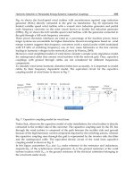
From fig. 11-b and fig. 12-b the difference between the main and the boundary operation
mode of the converter can be seen. In the first case, the commutations in the rectifier (the
process of recharging the capacitor С
0
) end before the commutations in the inverter (the
process of recharging the capacitor С
S
). In the second case, the commutations in the rectifier
complete after the ones in the inverter. In both cases during the commutations in the
rectifier, all of its diodes are closed and the output current i
0
is equal to zero (fig. 11-с and
fig. 12-с).
Fig. 12-b confirms the fact that at certain conditions the output voltage can become higher
than the power supply voltage without using a matching transformer.
At no-load mode, the converter operation is shown in fig. 13. In this case, the output voltage
is more than two times higher than the power supply one.
u
a
500V/div; u
b
500V/div; х=5µs/div
Fig. 13. Oscillograms, illustrating no-load mode of the converter
8. Conclusions
The operation of an LCC transistor resonant DC/DC converter with a capacitive output
filter and working above the resonant frequency has been investigated, taking into account
the influence of snubber capacitors and a matching transformer. The particular operation
modes of the converter have been considered, and the conditions under which they are
obtained have been described. The output characteristics for all operation modes of the
converter have been built including at regulation by means of changing the operating
frequency. The boundary curves between the different operation modes of the converter as
well as the area of natural commutation of the controllable switches have been shown in the
plane of the output characteristics. Results from investigations carried out by means of a
laboratory prototype of the converter have been obtained and these results confirm the ones
from the analysis.
The theoretical investigations show that the conditions for ZVS can be kept the same for
high-Ohm loads and the converter can stay fit for work even at a no-load mode. For the
purpose, it is necessary to have the natural capacity of the matching transformer bigger than
the one of the snubber capacitors.
The output characteristics show that in the zone of small loads the value of the normalized
output voltage increases to reach a value higher than unit what is characteristic for
Power Quality Harmonics Analysis and Real Measurements Data
130
converters with controllable rectifying. This can be explained by the similar mechanism of
the rectifier operation in the investigated converter.
The results from the investigation can be used for more precise designing of LCC converters
used as power supplies for electric arc welding aggregates, powerful lasers, luminescent
lamps etc.
9. References
Al Haddad, K., Cheron, Y., Foch, H. & Rajagopalan, V. (1986). Static and dynamic analysis of
a series resonant converter operating above its resonant frequency, Proceedings of
SATECH'86, pp.55-68, Boston, USA.
Bankov, N. (2009) Influence of the Snubbers and Matching Transformer over the Work of a
Transistor Resonant DC/DC Converter. Elektrotehnika&Elektronika (Sofia, Bulgaria),
Vol. 44, No. 7-8, pp. 62-68, ISSN 0861-4717.
Cheron, Y., Foch, H. & Salesses, J. (1985). Study of resonant converter using power
transistors in a 25-kW X-Rays tube power supply. IEEE Power Electronics Specialists
Conference, ESA Proceedings, 1985, pp. 295-306.
Cheron, Y. (1989). La commutation douce dans la conversion statique de l'energie electrique,
Technique et Documentation, ISBN : 2-85206-530-4, Lavoisier, France.
Malesani, L., Mattavelli, P., Rossetto, L., Tenti, P., Marin, W. & Pollmann, A. (1995).
Electronic Welder With High-Frequency Resonant Inverter. IEEE Transactions on
Industry Applications, Vol. 31, No.2, (March/April 1995), pp. 273-279, ISSN: 0093-
9994.
Jyothi, G. & Jaison, M. (2009). Electronic Welding Power Source with Hybrid Resonant
Inverter, Proceedings of 10th National Conference on Technological Trends (NCTT09),
pp. 80-84, Kerala, India, 6-7 Nov 2009.
Liu, J., Sheng, L., Shi, J., Zhang, Z. & He, X. (2009). Design of High Voltage, High Power and
High Frequency in LCC Resonant Converter. Applied Power Electronics Conference
and Exposition, APEC 2009. Twenty-Fourth Annual IEEE, pp. 1034-1038, ISSN: 1048-
2334, Washington, USA, 15-19 Feb. 2009.
Ivensky, G., Kats, A. & Ben-Yaakov, S. (1999). An RC load model of parallel and series-
parallel resonant DC-DC converters with capacitive output filter. IEEE Transactions
on Power Electronics, Vol. 14, No.3, (May 1999), pp. 515-521, ISSN: 0885-8993.
5
Thermal Analysis of Power
Semiconductor Converters
Adrian Plesca
Gheorghe Asachi Technical University of Iasi
Romania
1. Introduction
Power devices may fail catastrophically if the junction temperature becomes high enough to
cause thermal runaway and melting. A much lower functional limit is set by temperature
increases that result in changes in device characteristics, such as forward breakover voltage
or the recovery time, and failure to meet device specifications.
Heat generation occurs primarily within the volume of the semiconductor pellet. This heat
must be removed as efficiently as possible by some form of thermal exchange with the
ambient, by the processes of conduction, convection or radiation.
Heat loss to the case and heat-sink is primarily by conduction. Heat loss by radiation
accounts for only 1-2% of the total and can be ignored in most situations. Finally, loss from
the heat-sink to the air is primarily by convection. When liquid cooling is used, the heat loss
is by conduction to the liquid medium through the walls of the heat exchanger. Heat
transfer by conduction is conveniently described by means of an electrical analogy, as it
shows in Table 1.
THERMAL ELECTRICAL
Quantity Symbol Measure
unit
Quantity Symbol Measure
unit
Loss
power
P W Electric
current
I A
Temperature
variation
0
C Voltage U V
Thermal
resistance
R
th
0
C/W Electrical
resistance
R
Thermal
capacity
C
th
J/
0
C Electrical
capacity
C F
Heat Q J Electrical
charge
Q As
Thermal
conductivity
W/m
0
C Electrical
conductivity
1/m
Table 1. Thermal and electrical analogy
Power Quality Harmonics Analysis and Real Measurements Data
132
Taking into account the thermal phenomena complexity for power semiconductor devices it
is very difficult to study the heating processes both in steady-state or transitory operating
conditions, using the traditional analytical equations. The modeling concepts have their
strength for different grades of complexity of the power circuit. It is important to achieve an
efficient tradeoff between the necessary accuracy, required simulation speed and feasibility
of parameter determination, (Kraus & Mattausch, 1998). Approaches to simulate these
processes have already been made in earlier work. Numerical programs based on the
method of finite differences are proposed in (Wenthen, 1970), or based on formulation of
charge carrier transport equations, (Kuzmin et al., 1993). A physical model using the
application of continuity equation for description of the carrier transport in the low doped
layer of structures is proposed in (Schlogl et al., 1998). A simple calculation procedure for
the time course of silicon equivalent temperature in power semiconductor components
based on the previously calculated current loading is shown in (Sunde et al., 2006). In order
to take into account the nonlinear thermal properties of materials a reduction method based
on the Ritz vector and Kirchoff transformation is proposed in (Gatard et al., 2006).
The work described in (Chester & Shammas, 1993) outlines a model which combines the
temperature dependent electrical characteristics of the device with its thermal response. The
most papers are based on the thermal RC networks which use the PSpice software, (Maxim
et al., 2000; Deskur & Pilacinski, 2005). In (Nelson et al., 2006) a fast Fourier analysis to
obtain temperature profiles for power semiconductors is presented. Electro-thermal
simulations using finite element method are reported in (Pandya & McDaniel, 2002) or
combination with the conventional RC thermal network in order to obtain a compact model
is described in (Shammas et al., 2002). Most of the previous work in this field of thermal
analysis of power semiconductors is related only to the power device alone. But in the most
practical applications, the power semiconductor device is a part of a power converter
(rectifier or inverter). Hence, the thermal stresses for the power semiconductor device
depend on the structure of the power converter. Therefore, it is important to study the
thermal behaviour of the power semiconductor as a component part of the converter and
not as an isolated piece. In the section 2, the thermal responses related to the junction
temperatures of power devices have been computed. Parametric simulations for transient
thermal conditions of some typical power rectifiers are presented in section 3. In the next
section, the 3D thermal modelling and simulations of power device as main component of
power converters are described.
2. Transient thermal operating conditions
The concept of thermal resistance can be extended to thermal impedance for time-varying
situations. For a step of input power the transient thermal impedance, Z
thjCDC
(t), has the
expression,
jC
thjCDC
t
Zt
P
(1)
where:
Z
thjCDC
(t) means junction-case transient thermal impedance;
jC
(t) – difference of temperature between junction and case at a given time t;
P – step of input power.
The transient thermal impedance can be approximated through a sum of exponential terms,
like in expression bellow,
Thermal Analysis of Power Semiconductor Converters
133
1
1
j
t
k
thjCDC j
j
Ztre
(2)
where
jjj
rC
means thermal time constant.
The response of a single element can be extended to a complex system, such as a power
semiconductor, whose thermal equivalent circuit comprises a ladder network of the separate
resistance and capacitance terms shown in Fig. 1.
Fig. 1. Transient thermal equivalent circuit for power semiconductors
The transient response of such a network to a step of input power takes the form of a series
of exponential terms. Transient thermal impedance data, derived on the basis of a step input
of power, can be used to calculate the thermal response of power semiconductor devices for
a variety of one-shot and repetitive pulse inputs. Further on, the thermal response for
commonly encountered situations have been computed and are of great value to the circuit
designer who must specify a power semiconductor device and its derating characteristics.
2.1 Rectangular pulse series input power
Figure 2 shows the rectangular pulse series and the equation (3) describes this kind of input
power.
,
01
FM
PifnTtnT
Pt
i
f
nT t n T
(3)
Fig. 2.
Rectangular pulse series input power
The thermal response is given by the following equation,
Power Quality Harmonics Analysis and Real Measurements Data
134
1
1
1
1
1
11
1,
1
1
11
1
ii ii
i
i
ii
i
nT
tnT nT T
TT TT
k
FM i
T
i
T
jC n
nT
tnT
T
k
TT
FM i
T
i
T
ee ee
Pr ifnTtnT
e
t
e
Pre e ifnT tnT
e
(4)
For a very big number of rectangular pulses, actually n , it gets the relation:
1
1
1
1,
1
1
1
1
i
i
i
i
i
i
T
t
T
k
T
FM i
T
i
T
jC
t
T
k
T
FM i
T
i
T
e
Pre ifnTtnT
e
t
e
Pre ifnT tnT
e
(5)
Therefore, the junction temperature variation in steady-state conditions will be,
11 1
1
11
1
11
1
1
ii
ii
ii
i
i
TT
TT
kk k
TT
jC FM FM i FM i FM i
TT
ii i
TT
T
k
FM i
T
i
T
ee
PPrPre Pr e
TT
ee
e
Pr
T
e
(6)
2.2 Increasing triangle pulse series input power
A series of increasing triangle pulses is shown in Fig. 3 and the equation which describes
this series is given in (7).
Fig. 3. Increasing triangle pulse series input power
Thermal Analysis of Power Semiconductor Converters
135
,
01
FM
P
tifnTtnT
Pt
i
f
nT t n T
(7)
In the case when
n
, the thermal response will be,
1
1
11
1,
1
1
1
1
i
i
i
i
i
i
T
T
t
k
iT
FM
ii
T
i
T
jC
T
t
k
T
FM i
ii
T
i
T
e
T
P
rtT e if nT t nT
e
t
e
PT
rT e if nT t n T
e
(8)
2.3 Decreasing triangle pulse series input power
Figure 4 shows a decreasing triangle pulse series with its equation (9).
Fig. 4. Decreasing triangle pulse series input power
1,
01
FM
P
tifnTtnT
Pt
i
f
nT t n T
(9)
At limit, when n , the thermal response will be:
1
1
1
1,
1
11
1
1
i
i
i
i
i
T
T
t
k
T
FM i
ii
T
i
T
jC
T
k
i
FM
ii
T
i
T
e
PT
rtT e ifnTtnT
e
t
e
T
P
rT if nT t n T
e
(10)
Power Quality Harmonics Analysis and Real Measurements Data
136
2.4 Triangle pulse series input power
A series of triangle input power is shown in Fig. 5. The equation which describes this kind
of series is given in (11).
Fig. 5. Triangle pulse series input power.
,
22,
02 1
FM
FM
P
tifnTtnT
t
Pt P i
f
nT t nT
i
f
nT t n T
(11)
For junction temperature computation when n , the following relation will be used:
2
1
1
2
1
12
,
1
2
22,
1
1
1
ii
i
i
ii
i
i
i
i
TT
t
TT
k
T
FM
ii i
T
i
T
T
t
TT
k
T
FM
jC i i i
T
i
T
T
k
FM
ii
T
i
T
P
ee
rT e t T if nT t nT
e
P
ee
trT e tTi
f
nT t nT
e
e
P
rT
e
2
21
i
t
T
eifnTtnT
(12)
2.5 Trapezoidal pulse series input power
Figure 6 shows a trapezoidal pulse series with the equation from (13).
Thermal Analysis of Power Semiconductor Converters
137
Fig. 6. Trapezoidal pulse series input power
121
,
01
FM FM FM
t
PPP i
f
nT t nT
Pt
i
f
nT t n T
(13)
At limit,
n , the thermal response is given by,
12
12
21
1
1
1
1
,
1
1
1
1
i
i
i
i
t
k
PP
T
FM FM
ii FM i
T
i
T
jC
t
k
PP
T
ii
T
i
T
F
PP
rT e P t T if nT t nT
e
t
G
rT e if nT t n T
e
(14)
where:
12
12
21 12
12 21
11,
11
i
i
T
T
P P FM FM FM FM
ii
T
P P FM FM FM FM
ii
FPP PP e
TT
GPP PP e
TT
(15)
2.6 Partial sinusoidal pulse series input power
A partial sinusoidal pulse series waveform is shown in Fig. 7. The equation which describes
this kind of waveform is given by (16).
Power Quality Harmonics Analysis and Real Measurements Data
138
Fig. 7. Partial sinusoidal pulse series input power
sin ,
01
FM
PtifnTtnT
Pt
if nT t n T
(16)
In order to establish the junction temperature when
n , it will use the relation,
1
2
1
2
sin sin sin
11
,
sin sin
11
1
i
i
i
i
i
i
t
T
T
k
T
FM i i i
T
i
T
i
jC
t
T
k
T
FM i i i
T
i
T
i
e
PZ t r e
eT
if nT t nT
t
e
Pr e
eT
if nT t n T
(17)
where:
2
2
22
1
2
11
1
sin 2
1
2
;cos sin2;
2
cos
k
i
i
kk
ii
iiii
k
ii
i
ii
i
r
r
ctg Z r tg
T
r
(18)
Extremely short overloads of the type that occur under surge or fault conditions, are limited
to a few cycles in duration. Here the junction temperature exceeds its maximum rating and
all operational parameters are severely affected. However the low transient thermal
Thermal Analysis of Power Semiconductor Converters
139
impedance offered by the device in this region of operation, is often sufficient to handle the
power that is dissipated.
A transient thermal calculation even using the relation (2), is very complex and difficult to
do. Hence, a more exactly and efficiently thermal calculation of power semiconductors at
different types of input power specific to power converters, can be done with the help of
PSpice software and/or 3D finite element analysis.
3. Thermal simulations of power semiconductors from rectifiers
Further on, it presents the waveforms of input powers and junction temperatures of power
semiconductors, diodes and thyristors, from different types of single-phase bridge rectifiers.
Also, temperature waveforms in the case of steady state thermal conditions, are shown.
Using PSpice software, a parametric simulation which highlights the influence of some
parameter values upon temperature waveforms has been done.
On ordinate axis, the measurement unit in the case of input power waveforms, is the watt,
and in the case of temperatures, the measurement unit is the
0
C, unlike the volt one that
appears on graphics. This apparent unconcordance between measurement units is because
thermal phenomena had been simulated using electrical circuit analogy. The notations on
the graphics P
1
, P
2
and P
3
mean input powers and T
1
, T
2
and T
3
temperatures, respectively.
3.1 Single-phase uncontrolled bridge rectifier
The waveforms of the input powers and junction temperatures of power diodes from the
structure of a single-phase uncontrolled bridge rectifier are shown in the below diagrams.
Time
0s 20ms 40ms 60ms 80ms 100ms
V(MULT1:OUT)
0V
0.5KV
1.0KV
P3
P2
P1
Fig. 8. Input power waveforms at load resistance variation with 10, 20, 50Ω
From the above graphics, Fig. 8, the input power variation P
1
, P
2
and P
3
with the load
resistance values can be noticed. The increase of load values leads to small input power
values, and finally, to the decrease of junction temperature magnitudes, T
1
, T
2
and T
3
, Fig. 9,
and also to the decrease of temperature variations. In the case of quasi-steady state thermal
conditions, Fig. 10, there are a clearly difference between temperatures waveforms variation.
Also, the time variations of temperature values are insignificantly. The maximum value of
T
1
temperature, Fig. 10, outruns the maximum admissible value for power semiconductor
junction, about 125
0
C. Therefore, it requires an adequate protection for the power diode or
increasing of load resistance.
Power Quality Harmonics Analysis and Real Measurements Data
140
Time
0s 20ms 40ms 60ms 80ms 100ms
V(SUM1:OUT)
25.0V
37.5V
50.0V
62.5V
75.0V
T3
T2
T1
Fig. 9. Temperature waveforms of thermal transient conditions at load variation with 10, 20,
50Ω
Time
4.80s 4.85s 4.90s 4.95s 5.00s
V(SUM1:OUT)
50V
100V
150V
T3
T2
T1
Fig. 10. Temperature waveforms of quasi-steady state thermal conditions at load variation
with 10, 20,50Ω
3.2 Single-phase semicontrolled bridge rectifier
In the case of a single-phase semicontrolled bridge rectifier made with power diodes and
thyristors, the time variations of input powers and temperatures are presented below.
Time
0s 20ms 40ms 60ms 80ms 100ms
V(MULT1:OUT)
0V
125V
2
50V
3
75V
P3
P2
P1
Fig. 11. Input power waveforms at firing angle variation with 60, 90, 120
0
el.
Thermal Analysis of Power Semiconductor Converters
141
Time
0s 20ms 40ms 60ms 80ms 100ms
V(SUM1:OUT)
25.0V
31.3V
37.5V
43.8V
50.0V
T3
T2
T1
Fig. 12. Temperature waveforms of thermal transient conditions at firing angle variation
with 60, 90, 120
0
el.
Time
4.80s 4.85s 4.90s 4.95s 5.00s
V(SUM1:OUT)
50V
75V
1
00V
30V
T3
T2
T1
Fig. 13. Temperature waveforms of quasi-steady state thermal conditions at firing angle
variation with 60, 90, 120
0
el.
Time
0s 20ms 40ms 60ms 80ms 100ms
V(MULT1:OUT)
0V
250V
500V
750V
P3
P2
P1
Fig. 14. Input power waveforms at load inductance variation with 0.1, 10, 50mH
It has been done a parametric simulation both at firing angle variation of thyristors from
semicontrolled bridge rectifier, Fig. 11…13, and at load inductance variation, Fig. 14…16.
As in previous situation, the case with uncontrolled bridge rectifier, the variation of input
power values depend on load inductance, Fig. 14. The increase of inductance value, from
Power Quality Harmonics Analysis and Real Measurements Data
142
0.1mH to 50mH, leads not only to input power decreasing, P
3
< P
2
< P
1
, but also its shape
changing. The same thing can be observed at firing angle variation, Fig. 11 13. Hence, the
increase of the firing angle from 60 to 120
0
el., leads to decrease of input power values P
3
<
P
2
< P
1
. Also, the increase of load inductance leads to decrease of temperature values, T
3
< T
2
< T
1
, as shown in Fig. 15 and Fig. 16. The steady state thermal conditions allow to highlight
the temperature differences in the case of firing angle variation, T
3
< T
2
< T
1
, Fig. 13, and
load variation, T
3
< T
2
< T
1
, Fig. 16.
Time
0s 20ms 40ms 60ms 80ms 100ms
V(SUM1:OUT)
25.0V
37.5V
50.0V
60.0V
T3
T2
T1
Fig. 15. Temperature waveforms of thermal transient conditions at load inductance variation
with 0.1, 10, 50mH
Time
4.80s 4.84s 4.88s 4.92s 4.96s 5.00s
V(SUM1:OUT)
50V
75V
1
00V
T3
T2
T1
Fig. 16. Temperature waveforms of quasi-steady state thermal conditions at load inductance
variation with 0.1, 10, 50mH
3.3 Single-phase controlled bridge rectifier
Next diagrams present input power variation and temperature values in the case of a single-
phase controlled bridge rectifier made with power thyristors.
As in the case of single-phase semicontrolled bridge rectifier, a parametric simulation for
firing angle variation has been done. It can be noticed that increasing of firing angle leads to
input power and temperature decrease, Fig. 17 and Fig. 18. The quasi-steady state thermal
conditions highlight the differences between temperature values and their variations, Fig.
19. In order to validate the thermal simulations some experimental tests have been done. It
was recorded the temperature rise on the case of the thyristors used for semi-controlled
Thermal Analysis of Power Semiconductor Converters
143
power rectifier. The temperatures have been measured using proper iron-constantan
thermocouples fixed on the case of power semiconductor devices. The measurements have
been done both for the firing angle values of 60, 90 and 120
0
el., and load inductance values
of 0.1, 10 and 50mH. The results are shown in Fig. 20 and Fig. 21.
Time
0s 20ms 40ms 60ms 80ms 100ms
V(MULT1:OUT)
0V
250V
500V
750V
P3
P2
P1
Fig. 17. Input power waveforms at firing angle variation with 60, 90, 120
0
el.
Time
0s 20ms 40ms 60ms 80ms 100ms
V(SUM1:OUT)
37.5V
50.0V
62.5V
T3
T2
T1
Fig. 18. Temperature waveforms of thermal transient conditions at firing angle variation
with 60, 90, 120
0
el.
T
ime
4.80s 4.85s 4.90s 4.95s 5.00s
V(SUM1:OUT)
50V
75V
100V
30V
T3T2T1
Fig. 19. Temperature waveforms of quasi-steady state thermal conditions at firing angle
variation with 60, 90, 120
0
el.
Power Quality Harmonics Analysis and Real Measurements Data
144
0
10
20
30
40
50
60
0 100 200 300 400 500 600 700
t[s]
T[ºC]
60el.sim 90el.sim 120el.sim 60el.exp 90el.exp 120el.exp
Fig. 20. Comparison between simulation and experimental temperature rise of the case at
firing angle variation
0
10
20
30
40
50
60
70
0 100 200 300 400 500 600 700
t[s]
T[ºC]
L1sim L2sim L3sim L1exp L2exp L3exp
Fig. 21. Comparison between simulation and experimental temperature rise of the case at
inductance load variation
In both cases, at firing angle and load inductance variation, it ca be noticed closer values
between simulation results and measurements. Of course, there are different temperature
Thermal Analysis of Power Semiconductor Converters
145
values resulted from experimental tests (60el.exp, 90el.exp and 120el.exp from Fig. 20 and
L1exp, L2exp, L3exp as shown in Fig. 21) with respect to simulations (60el.sim, 90el.sim and
120el.sim from Fig. 20 and L1sim, L2sim, L3sim as in Fig. 21), because of measurement
errors, thermal model simplifications and mounting test conditions. Anyway, the maximum
difference between experimental and simulation results is less than 3ºC.
3.4 D thermal modelling and simulations of power semiconductors
During former work, (Chung, 1999; Allard et al., 2005), because of limited computer
capabilities, the authors had to concentrate on partial problems or on parts of power
semiconductors geometry. The progress in computer technology enables the modelling and
simulation of more and more complex structures in less time. It has therefore been the aim
of this work to develop a 3D model of a power thyristor as main component part from
power semiconductor converters.
The starting point is the power balance equation for each volume element dV, in the integral
formulation:
2
()
j
T
dV c dV div
g
radT dV
t
(19)
where:
T means the temperature of element [ºC];
j – current density [A/m
2
];
σ – electrical conductivity [1/Ωm];
ρ – material density [kg/m
3
];
c – specific heat [J/kgºC];
λ – thermal conductivity [W/mºC].
The left term of before equation (it exists only in the device conductor elements), denotes the
heating power from the current flow. It is in balance with the heat stored by temporal
change of temperature, and the power removed from the element by thermal conduction.
For the steady state temperature calculation, the heat storage term is zero, and the equation
(19) becomes,
2
()
j
dV div
g
radT dV
(20)
Taking one's stand on the above thermal equations, first of all a 3D model for a power
thyristor has been developed using a specific software, the Pro-ENGINEER, an integrated
thermal design tool for all type of accurate thermal analysis on devices.
It has been considered an application which includes a bidirectional bridge equiped with
power thyristors type AT505, with the average direct current of 430A and an internal
resistance of 0.68m. The current which flows through the converter branches is about
315A. This value allows computing the power loss for each tyristor, which results in 67.47W.
The material properties of every component part of the thyristor are described in the Table 2
and the 3D thermal models of the thyristor with its main component parts and together with
its heatsinks for both sides cooling are shown in Fig. 22, respectively, Fig. 23.
Power Quality Harmonics Analysis and Real Measurements Data
146
Fig. 22. Thermal model of the thyristor (1 – cathode copper pole; 2 – silicon chip;
3 – molybdenum disc; 4 – anode copper)
Fig. 23. Thermal model of the assembly thyristor - heatsinks
1
2
3
4
Thermal Analysis of Power Semiconductor Converters
147
The thermal model of the power semiconductor has been obtained by including all the piece
part that is directly involved in the thermal exchange phenomenon, which is: anode copper
pole, molybdenum disc, silicon chip, cathode copper pole, Fig. 22. The device ceramic
enclosure has not been included in the model since the total heat flowing trough it is by far
less important than the heat flowing through the copper poles. All the mechanical details
which are not important for the heat transfer within the thyristor and from the thyristor to
the external environment (e.g. the centering hole on the poles) have been suppressed.
Parameter
Material
Co
pp
er Silico
n
Mol
y
bdenum Aluminium
(
k
g
/m
3
)
8900 2330 10220 2700
c
(
J/k
g
ºC
)
387 702 255 900
(W/mºC)
385 124 138 200
Table 2. Material Data and Coefficients at 20ºC
The heat load has been applied on the active surface of the silicon of power semiconductor.
It is a uniform spatial distribution on this surface. The ambient temperature was about 25ºC.
From experimental tests it was computed the convection coefficient value, k
t
=
14.24W/m
2
ºC for this type of heatsinks for thyristor cooling. Hence, it was considered the
convection condition like boundary condition for the outer boundaries such as heatsinks.
The convection coefficient has been applied on surfaces of heatsinks with a uniform spatial
variation and a bulk temperature of 25ºC. The mesh of this 3D power semiconductor
thermal model has been done using tetrahedron solids element types with the following
allowable angle limits (degrees): maximum edge: 175; minimum edge: 5; maximum face:
175; minimum face: 5. The maximum aspect ratio was 30 and the maximum edge turn
(degrees): 95. Also, the geometry tolerance had the following values: minimum edge length:
0.0001; minimum surface dimension: 0.0001; minimum cusp angle: 0.86; merge tolerance:
0.0001. The single pass adaptive convergence method to solve the thermal steady-state
simulation has been used.
Then, it has been made some steady-state thermal simulations for the power semiconductor.
For all thermal simulations a 3D finite elements Pro-MECHANICA software has been used.
The temperature distribution of the tyristor which uses double cooling, both on anode and
cathode, is shown in the pictures below, Fig. 24 and Fig. 25. The maximum temperature for
the power semiconductor is on the silicon area and is about 70.49ºC and the minimum of
47.97ºC is on the heatsink surfaces.
Further on, the thermal transient simulations have been done in order to compute the
transient thermal impedance for power thyristor. The result is shown in Fig. 26.
From thermal transient simulations we obtain the maximum temperature time variation and
the minimum temperature time variation. From the difference between maximum
temperature time variation and ambient temperature divided to total thermal load it gets
the thermal transient impedance. Dividing the thermal transient impedance to the thermal
resistance, the normalised thermal transient impedance can be obtained. This is a thermal
quantity which reflects the power semiconductor thermal behaviour during transient
conditions.
To understand and to optimize the operating mechanisms of power semiconductor
converters, the thermal behaviour of the power device itself and their application is of major
interest. Having the opportunity to simulate the thermal processes at the power
Power Quality Harmonics Analysis and Real Measurements Data
148
Fig. 24. Temperature distribution through the thyristor mounted between heatsinks at 50%
cross section, yz plane
Fig. 25. Temperature distribution through the thyristor mounted between heatsinks at 50%
cross section, xz plane
