Optoelectronics Materials and Techniques Part 14 doc
Bạn đang xem bản rút gọn của tài liệu. Xem và tải ngay bản đầy đủ của tài liệu tại đây (3.45 MB, 30 trang )
Air Exposure Improvement of Optical Properties of Hydrogenated
Nanostructured Silicon Thin Films for Optoelectronic Application
379
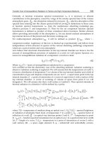
Fig. 2 shows the (110) average grain size obtained from the <110> x-ray diffraction
spectra, for as deposited films (closed triangles) and exposed to air for two months films
(closed circles), respectively, as a function of deposition temperature. As shown in Fig. 2,
with decreasing deposition temperature the average grain size, <δ>, decreases. We can
also see the effect of air exposure. When the time of air exposure increases, as shown in
this diagram, it is found that the <δ> values decrease. It is clear that the positive shift of
Raman-peak with deposition temperature is in good agreement with the increase of grain
size with deposition temperature. In other words, according to a phonon confinement
effect, the upshift of phonon peak is due to the increase of the hydrogenated
nanostructured silicon grains size.
21
[H2] = 20 sccm
<δ(110)> (nm)
18
15
12
As-deposited
9
After two months
6
50
100
150
200
250
300
o
Deposition Temperature ( C)
Fig. 2. Average grain size, <δ(110)> obtained from <110> X-ray diffraction spectra as a
function of deposition temperature, for as deposited films (closed triangles) and exposed
films to air for two months (closed circles)
For growth of crystallites in hydrogenated nanostructured silicon thin films, SiH-related
adsorbates responsible for the film growth must move on the growing surface until the
adsorbates find the lattice sites for forming the crystallites with a given texture. According
to the model proposed by Matsuda (Matsuda, 1983), high deposition temperature
conditions should decrease the surface migration rate for eliminating the crystalline
phases from films. However, as seen in Fig. 2, small grains grown in the films with
deposition temperature higher than 60 °C. Furthermore, the density of SiH-related bonds
monotonically decreases with deposition temperature, as shown later. These results
suggest that an increase in deposition temperature causes an increase in the surface
migration rate, in contrast with the model proposed by Matsuda (Matsuda, 1983). Thus,
380
Optoelectronics - Materials and Techniques
we can obtain silicon films including nanometer-sized crystallites by decreasing
deposition temperature, as seen in Fig. 2, which have attracted increased interested as
optoelectronic materials. This is because the decrease in the deposition temperature will
suppress the surface migration of the adsorbates as precursors for creating a crystalline
phase as stated above.
The surface morphology of the thin films prepared with different deposition temperature
(Figs. 3a and 3b) and the time of air exposure (Figs. 3b and 3c) has been measured by atomic
force microscopy, as shown in Fig. 3. It can be seen clearly from Fig. 3a that the surface is
almost flat corresponds to the amorphous tissue in good agreement with the result from
Raman data (Fig. 1). On the other hand, it can be seen from Fig. 3b and 3c that the ship of the
grains on the surface is spherical. In addition, the nanocrystallites of the silicon are
distributed nearly uniform over the surface and hence suitable for integration in device
structure. It is therefore expected that grown thin films could be used as protective coatings
in device. The average grain size values estimated from atomic force microscopy data in
Fig. 3b are larger than that in Fig. 3c, in good agreement with that calculated from the
Scherrer’s formula (Fig. 2).
a
b
c
40 nm
40 nm
Fig. 3. The atomic force microscopy (AFM) pictures of deposited silicon thin films at
[H2]
= 20 sccm. (a) The AFM of sample deposited at deposition temperature (Td) of 60 oC. (b) The
AFM of sample deposited at Td of 150 oC before air exposure (as-deposited). (c) The AFM of
sample deposited at Td of 150 oC after two months air exposure
It is well known that when polycrystalline silicon or hydrogenated nanostructured silicon is
used as a gate electrode or an interconnection material in integrated circuits, the undesirable
oxidation results in a limitation of its conductivity and finally can degrade circuit
performance. Furthermore, the grain boundaries in the polycrystalline silicon or
hydrogenated nanostructured silicon, which has disordered structures including weak
bonds, are expected to oxidize more rapidly than the inside of the grains with stable
structure. By using Fourier-transform infrared spectroscopy measurement, we investigated
the stability and the oxidation rates of some selected samples with different structures. To
investigate the oxidation rates of these films we measured them again after two months.
Fig. 4 reports the Fourier-transform infrared transmission spectra of the hydrogenated
nanostructured silicon films deposited at different deposition temperature, Fig. 4a for as
deposited films and Fig. 4b as the results after air exposure for two months. Firstly,
considering the virgin (as deposited) samples (Fig. 4a), the spectra observed at around
650 cm-1 and 950-980 cm-1 are assigned to the rocking/wagging and bending vibration
Air Exposure Improvement of Optical Properties of Hydrogenated
Nanostructured Silicon Thin Films for Optoelectronic Application
381
Transmittance (a.u.)
modes of (Si3)-SiH bonds, respectively (Kroll et al., 1996). The stretching mode of Si-F
vibration is also located at 800-900 cm-1.
(Si-F)str
Td = 300 o C
o
150 C
o
80 C
(Si-H)str
[H2] = 20 sccm
(Si-H)ben
(S i-H)wag
a
3000
4000
2000
1000
400
-1
Transmittance (a.u.)
Wavenumber (cm )
Td = 300 o C
150 o C
o
80 C
(C-H n )str
(Si-O )
str
b
4000
3000
2000
1000
400
-1
Wavenumber (cm )
Fig. 4. Infrared transmittance spectra for hydrogenated nanostructured silicon thin films
with different deposition temperature (Td) values. (a) As-deposited and (b) After two
months air exposure
382
Optoelectronics - Materials and Techniques
The peak at 2100 cm-1 is assigned to the dihydride, ((Si2)–SiH2) (Itoh et al., 2000), chain
structure in the grain boundaries, or gathered (Si3)–SiH bonds on the surface of a large void
(Street, 1991), in which silicon dangling bonds are included and makes a porous structure.
The intensity of the spectra at around 2100 cm-1 is likely to decreases with increasing
deposition temperature. So, the hydrogen content decreases with increasing deposition
temperature. The hydrogen atoms in the hydrogenated nanostructured silicon thin films are
suggested to reside mostly in the grain boundary region. On the other hand, we can see the
films after two months air exposure exhibit a more oxidation (see Fig. 4b). The spectra
observed at around 1100 cm-1 and 2700-3000 cm-1 are assigned to the stretching mode of
Si-O-Si vibration and (CH) stretching, respectively (San Andre´s et al., 2003). The oxygen
absorption peak increases abruptly (see Fig. 4b). The presence of oxygen in the
hydrogenated nanostructured silicon thin films is probably due to the oxidation at the grain
boundaries, that is why <δ> values decrease in the films exposed to air for two months, as
seen in Fig. 2 (closed circles).
A comparison between the virgin (as deposited) samples, corresponding to Fig. 4a, and
those measured after two months, corresponding to 4b, shows a reduction in the (Si3)–SiHrelated peaks at 2100 and 630 cm-1 and leads to an increase in the Si–O–Si vibration at
1064 cm-1 after two months. For interpreting an increase in Si–O–Si peaks for samples
measured after air exposure, we could consider the following assumption: The oxygen
atoms can be replaced with hydrogen atoms on the surface of void structure in the grain
boundaries or those in amorphous-like regions between the grains. Then, we assume that
some of the oxygen atoms, supplied from O2 in the air, react with the SiH bonds and leaving
H2O or H2 behind.
4. Optical properties
4.1 Photoluminescence
The photoluminescence spectra are plotted in Fig. 5, 5a as deposited and 5b exposed to air
for two months, respectively, as a function of photon energy for various films. They exhibit
two separated photoluminescence bands: One is a relatively strong photoluminescence band
with peak energy at around 1.75-1.78 eV (708-696 nm) and the other is a weak band at
around 2.1-2.3 eV (590-539 nm). Both of these peaks are at energies above the band gap
energy for crystalline silicon (1.12 eV at room temperature) which has an indirect band gap
and is also not expected to luminescence in the visible range. In addition, Fig. 5 shows the
dependence of photoluminescence spectrum on the deposition temperature and the time of
air exposure. As the deposition temperature decreases and the time of air exposure increases
the photoluminescence intensity and photoluminescence peak energy values increase, i.e.,
photoluminescence improved with air exposure. It is noted that the photoluminescence
spectra from this nanocrystalline silicon were very broad, and that as the nanocrystal size
was reduced, photoluminescence broadening accompanied photoluminescence blue shift.
The width of the observed photoluminescence could be explained by the distributions of
sizes in our hydrogenated nanostructured silicon, and therefore of energy gaps. As seen in
Figs. 2, 4 and 5, the increase in the photoluminescence intensity and the peak energy with
decreasing deposition temperature and increase the time of air exposure is found to
correspond well with a decrease in <δ> (see Fig. 2 and an increase in the intensities of the
2100-cm-1-infrared-absorption bands (see Fig. 4a and 1100-cm-1-infrared-absorption bands
(see Fig.4b).
Air Exposure Improvement of Optical Properties of Hydrogenated
Nanostructured Silicon Thin Films for Optoelectronic Application
383
PL Intensity (a.u.)
[H2] = 20 sccm
a
o
Td = 80 C
o
150 C
o
300 C
1.4
1.6
1.8
2.0
2.2
2.4
2.6
Photon Energy (eV)
PL Intensity (a.u.)
b
o
Td = 80 C
o
150 C
o
300 C
1.4
1.6
1.8
2.0
2.2
2.4
2.6
Photon Energy (eV)
Fig. 5. Photluminescence (PL) spectra for hydrogenated nanostructured silicon thin films
with different deposition temperature values. (a) As-deposited and (b) After two months air
exposure
In addition, no photoluminescence is observed for the film as deposited at 60 oC, which was
amorphous as seen in Fig. 1. Therefore, it is considered that an amorphous silicon phase is
not responsible for the observed luminescence in the present work. The origin of the first
384
Optoelectronics - Materials and Techniques
peak (1.75-1.78 eV) may be ascribed to nanometersized grains, that is, the
photoluminescence peak energy value for this band increases with a decrease in the <δ>
value (Fig. 1b). And the origin of second peak (2.1-2.3 eV) may be due to defect related
oxygen (Fig. 2). On the other hand, it has been suggested that the exciton localization at the
Si/SiO2 interface is important in determining the photoluminescence process for both 1.65
and 2.1 eV bands (Kanemitsu et al., 2000). In addition, the photoluminescence bands for Hpassivated nanocrystalline silicon films show red shifts after passivation, in contrast to the
cause of O-passivated films that show blue shifts after passivation (Dinh et al., 1996) in good
agreement with the present work. Moreover, It has been widely established that the origins
of photoluminescence from amorphous silicon dioxide are oxygen-vacancies (E' center,
normally denoted by O≡Si–Si≡O) (Kenyon et al., 1994; Zhu et al., 1996) and nonbridging
oxygen hole (NBOH) center, denoted by ≡Si–O) (Munekuni et al., 1990; Nishikawa et al.,
1996). Photoluminescence from E' center peaks at 2.0–2.2 eV and from nonbridging oxygen
hole peaks at 1.9 eV, covering the range from 1.55-2.25 eV. Oxygen–vacancies in fact joint
two Si3+, and nonbridging oxygen hole, Si4+ with a dangling bond at one oxygen atom. So
the intensity of photoluminescence from E' centers should be in proportion to the amount of
Si3+, and the photoluminescence intensity from nonbridging oxygen hole should be in
proportion to the amount of defect Si4+, which is in fact Si4+ containing a dangling bond, and
will diminish if this dangling bond combines with other silicon atom (Fang et al., 2007).
4
5x10
-1
Absorption Coefficient (cm )
4
4x10
4
3x10
a
Td=80 oC
o
Td=150 C
Td=300 oC
4
2x10
4
1x10
[H2] = 20 sccm
4
5x10
4
4x10
4
3x10
4
2x10
4
1x10
0
2.0
b
2.2
2.4
2.6
2.8
3.0
Energy (eV)
Fig. 6. Absorption coefficient as a function of photon energy for hydrogenated
nanostructured silicon thin films deposited at various deposition temperature (Td). (a) Asdeposited and (b) After two months air exposure
Air Exposure Improvement of Optical Properties of Hydrogenated
Nanostructured Silicon Thin Films for Optoelectronic Application
385
4.2 Absorption spectroscopy
Fig. 6 shows the absorption coefficient of the hydrogenated nanostructured silicon thin films
deposited at various deposition temperatures, as a function of photon energy. As seen in
Fig. 6, the curves are shifted to higher energy as deposition temperature decreases and after
two months air exposure, which implies that for a given photon energy, the films became
increasingly transparent with decreased deposition temperature and after two months air
exposure. Fig. 7 illustrates the values of (αhυ)1/2 versus photon energy for hydrogenated
nanostructured silicon thin films deposited at different deposition temperature. From these
curves, the optical band gaps can be obtained from the Tauc equation. The optical band gap
decreases as the deposition temperature increases. This expected behavior could be
explained by the change of size and the number of the formed particles with the variation of
deposition temperature. In addition, the present materials have a wide optical band gap.
Thus, the increase in optical band gap (Fig. 7) corresponds with a decrease in the grain size
as shown in Fig. 2. Other theoretical and experimental researches attribute this phenomenon
at the quantum confinement effect, e.g. the gap energy is conditioned on the size of the
nanocrystals.
400
[αhν]
1/2
(cm-1/2 eV1/2)
300
[H2] = 20 sccm
200
100
a
0
400
300
Td=80 oC
Td=150 oC
Td=300 oC
200
100
b
0
2.0
2.2
2.4
2.6
2.8
3.0
Energy (eV)
Fig. 7. Curves of (αhυ)1/2 vs. photon energy for hydrogenated nanostructured silicon thin
films (a) As-deposited and (b) After two months air exposure
386
Optoelectronics - Materials and Techniques
4.3 Band gap based on simple theory
Fig. 8 shows (a) the optical band gap, Egopt, and (b) photoluminescence peak energy, EPL, of
the 1.7–1.75-eV band observed for hydrogenated nanostructured silicon films deposited at
different [H2], as a function of deposition temperature. The Egopt values were determined by
drawing the Tauc plots, (αhυ)1/2 versus (hυ – Egopt), using the optical absorption coefficient, α,
observed at photon energy of hυ. As revealed in Fig. 8, an increase in EPL corresponds well
with an increase in Egopt with varying deposition temperature or [H2], though the rates in the
increase of EPL is considerably smaller than that of Egopt. This result suggest that the radiative
recombination between excited electron and hole pair, may be caused by states other than
those at both the band edges.
[H2] = 30 sccm
[H2] = 46 sccm
2.2
a
2.1
g
E opt (eV)
2.3
2.0
1.75
EPL (eV)
b
1.74
1.73
100
150
200
Deposition Temperature
250
(oC)
Fig. 8. (a) Optical band gap, Egopt, and (b) the peak energy, EPL, of the 1.7-1.75-eV
photoluminescence band observed for hydrogenated nanostructured silicon films deposited
at different [H2], as a function of deposition temperature.
In this section, we will discuss the band gap estimated using the shifts of the Raman spectra
that will reflect the characteristics of the whole grains with different size as well as the
photoluminescence and the optical absorption measurements. As shown in Fig. 1, the
Raman peak arising from crystalline phases shifts toward a low frequency side with
Air Exposure Improvement of Optical Properties of Hydrogenated
Nanostructured Silicon Thin Films for Optoelectronic Application
387
decreasing deposition temperature. Supposing that the peak shift is due only to the
confinement of optical phonons in spherical nanocrystals, we can estimate the crystallite size
in diameter, DR, as (Edelberg et al., 1997):
DR = 2π(B / Δυ)1 / 2
(1)
where B is 2.24 cm-1 nm2, and Δυ the frequency shift in unit of cm-1, which was defined as
the difference between the observed peak-frequency value and 522 cm-1. The latter value
was observed for single crystal silicon. Fig. 9 shows a relationship between <δ(111)> and
<δ(110)>, and DR.
Average Grain Size (nm)
24
<111>, [H2]=30 sccm
21
<111>, [H2]=46 sccm
<110>, [H2]=30 sccm
<110>, [H2]=46 sccm
18
15
12
9
6
0
2
4
6
8
DR (nm)
Fig. 9. Relationship between the average grain size, <δ(111)> and <δ(110)>, as a function of
the diameter of grains, DR, calculated using equation (1). The solid lines were drawn, using a
method of the least square
When we compared the results obtained under a given crystal direction and a given [H2],
we can find a close correlation between the <δ> and DR values. However, it is found that the
absolute values of <δ> observed are considerably larger than DR values and the rate in the
increase of <δ> are faster than that of DR, Furthermore, based on the results shown in Fig. 9,
we find a relationship of <δ> = 3.69 DR – 7.28 (nm) for the films with [H2] = 30 sccm and of
<δ> = 3.56 DR – 11.89 for the films with [H2] = 46 sccm, in the measurements under a
direction of the <110> axis that is the dominant texture in the films. On the other hand, for
the <111> texture, we find a relationship of <δ> = 2.61 DR + 4.48 for [H2] = 30 sccm and. <δ>
= 2.64 DR + 0.05 for [H2] = 46 sccm. These formulas were obtained by fitting the values of
<δ> vs. DR to a linear relationship, using a method of the least square. As seen in these
results, the linear relationships of <δ> as a function of DR appear to be characterized by the
crystal axis of grains, that is, the slope (3.63 ± 0.07) for the <110> texture is steeper than that
(2.63 ± 0.02) for the <111> texture.
388
Optoelectronics - Materials and Techniques
E, E opt or EPL (eV)
g
2.4
2.1
1.8
1.5
1.2
0.9
Eq. (2)
opt
E g at [H2] = 30 sccm
0.6
opt
E g at [H2] = 46 sccm
EPL at [H2] = 30 sccm
0.3
0.0
EPL at [H2] = 46 sccm
0
1
2
3
4
5
6
7
R (nm)
Fig. 10. Lowest excitation energy, E, as a function of R (a solid curve), obtained based on
equation 2. In this diagram, the experimental values of Egopt values (closed symbols) and EPL
(open symbols) values, which were shown in Figs. 8a and 8b, respectively, are also shown
for comparison, as a function of R(=DR/2) through the DR values obtained using the
experimental Δυ values along with equation 2
Using the values of DR for the individual samples, we can evaluate the lowest excitation
energy, E, under a simple confinement theory for electron and hole (Efros et al., 1982;
Kayanuma, 1988; Edelberg et al., 1997) as follows:
E = Eg + 2π 2h 2 / mr DR 2 – 3.572e 2 / εr DR + 0.284ERy
(2)
where Eg is the energy gap of crystalline silicon (1.12 eV at room temperature), R(=DR/2) is
the radius of crystals, mr is the reduced effective mass of an electron-hole pair, εr is the
dielectric constant, and ERy is the Rydberg energy for the bulk semiconductor. The value of E
correspond to the band gap of the films .In the later two terms, 3.572e2/εrDR corresponds to
the coulomb term and 0.284ERy gives the spatial correlation energy. The later two terms are
minor corrections, so we neglected them in the calculation used in this work, because the
contribution of these two terms to the total energy will be less than 5%(Edelberg et al., 1997).
Air Exposure Improvement of Optical Properties of Hydrogenated
Nanostructured Silicon Thin Films for Optoelectronic Application
389
Fig. 10 shows the E values (a solid curve) obtained based on equation 2, as a function of R.
In Fig. 10, the experimental values of Egopt (closed symbols) and EPL (open symbols) shown in
Figs. 9a and 9b, respectively, are also shown for comparison, as a function of R through the
values of DR obtained using the experimental Δυ values along with equation 1.
As shown in Fig. 10, we can find a qualitative agreement between the observed Egopt values
(closed triangles and closed circles) and a solid curve calculated using equation 2, though
the former values are considerably larger than the latter. Furukawa and Miyasato
(Furukawa & Miyasato, 1988) have found also similar discrepancy between the theoretical
and experimental results, and interpreted the discrepancy in terms of a difference in the
surface shape of grains as boundary conditions in both the theoretical and experimental
process. On the other hand, the change of EPL as a function of R is considerably smaller than
those of E and Egopt though the trend of the changes for EPL agreed with that for Egopt. This
result indicates that the photoluminescence process of the 1.7–1.75-eV band can not be
connected with the transition between both the band edges, related to formation of
nanocrystals.
5. Conclusion
Hydrogenated nanostructured silicoin thin films were deposited by plasma-enhanced
chemical vapor deposition. The luminescent characteristics of nc-Si and oxidized
Hydrogenated nanostructured silicoin thin films were studied in detail by means of the
photoluminescence, optical absorption, X-ray diffraction, atomic force microscopy and
Raman scattering analyses. After oxidation the size of crystallites is reduced thus enhancing
the quantum confinement to increase the luminescent intensity. The presence of
nanocrystals induces a widening of energy gap. The widening of the optical band gap can be
explained by a quantum size effect.
6. Acknowledgment
Financial support by King Abdulaziz City for Science and Technology under Grant number:
08-NAN153-7 is gratefully acknowledged.
7. References
Belomoin, G.; Therrien, J.; Smith, A.; Rao, S.; Twesten, R.; Chaieb, S.; Nayfeh, M.H.; Wagner,
L. & Mitas, L. (2002). Observation of a Magic Discrete Family of Ultrabright Si
Nanoparticles, Applied Physics Letters, Vol.80, No.5, (February 2002), pp. 841-843.
ISSN 0003-6951
Benyoucef, M.; Kuball, M.; Sun, J. M. ; Zhong, G. Z. & Fan, X. W. (2001). Raman Scattering
and Photoluminescence Studies on Si/SiO2 Superlattices, Journal of Applied Physics,
Vol.89, No.12, (June 2001), pp. 7903-7907, ISSN 0021-8979
Brongersma, M.L.; Polman, A.; Min, K.S.; Boer, E.; Tambo, T. & Atwater, H.A. (1998). Tuning
the Emission Wavelength of Si nanocrystals in SiO2 by Oxidation, Applied Physics
Letters, Vol.72, No.20 (May 1998), pp. 2577-2579, ISSN 0003-6951
Canham, L.T. (1990). Silicon Quantum Wire Array Fabrication by Electrochemical and
Chemical Dissolution of Wafers, Applied Physics Letters, Vol.57, No.10, (September
1990), pp.1046-104.8, ISSN 0003-6951
390
Optoelectronics - Materials and Techniques
Chaudhuri, P. & Das, U.K. (1995). Control of Microstructure and Optoelectronic Properties
of Si:H Films by Argon Dilution in Plasma-Enhanced Chemical Vapor Deposition
from Silane, Japanese Journal of Applied Physics, Vol.34, No.7A, (July 1995), pp. 34673473, ISSN 0021-4922
Cheng, Q.; Xu, S.; Chai, J.W.; Huang, S.Y.; Ren, Y.P.; Long, J.D.; Rutkevych, P.P. & Ostrikov,
K. (2008). Influence of Hydrogen Dilution on the Growth of Nanocrystalline Silicon
Carbide Films by Low-frequency Inductively Coupled Plasma Chemical Vapor
Deposition, Thin Solid Films, Vol.516, No.18, (July 2008), pp. 5991-5995, ISSN 00406090
Cohen, M. (Ed.). (1978). Elements of X-ray Diffraction, Addison-Wesley, ISBN 0201011743,
Massachusetts
Das, U. K.; Chaudhuri, P. & Kshirsagar, S. T. (1996). Effect of Argon Dilution on the
Structure of Microcrystalline Silicon Deposited from Silane, Journal of Applied
Physics, Vol.80, No.9, (November 1996), pp. 5389-5397, ISSN 0021-8979
Dinh, L.N.; Chase, L.L.; Baloch, M.; Siekhaus, W. J. & Wooten, F. (1996). Optical Properties
of Passivated Si Nanocrystals and SiOx Nanostructures, Physical Review B, Vol.54,
No.7, (August 1996), pp. 5029–5037, ISSN 1098-0121
Edelberg, E.; Bergh, S.; Naone, R.; Hall, M. & Aydil, E .S. (1997). Luminescence from Plasma
Deposited Silicon Films, Journal of Applied Physics, Vol. 81, No.5, (March 1997), pp.
2410-2417, ISSN 0021-8979
Efros, Al.L. & Efros, A.L. (1982). Interband Absorption of Light in a Semiconductor Sphere,
Soviet Physics-Semiconductors, Vol.16, (1982), pp. 772-775
Ehbrecht, M.; Ferkel, H.; Huisken, F.; Holz, L.; Polivanov, Y.N.; Smirnov, V.V.; Stelmakh,
O.M. & Schmidt, R. (1995). Deposition and Analysis of Silicon Clusters Generated
by Laser Induced Gas Phase Reaction, Journal of Applied Physics, Vol.78, No.9,
(November 1995), pp. 5302-5306, ISSN 0021-8979
Fang, Y.C.; Zhang, Z. J. & Lu, M. (2007). Room Temperature Photoluminescence Mechanism
of SiOx Film after Annealing at Different Temperatures, Journal of Luminescence,
Vol.126, No.1, (September 2007), pp. 145-148, ISSN 0022-2313
Funde, A.M.; Bakr, N.A.; Kamble, D.K.; Hawaldar, R.R.; Amalnerkar, D.P. & Jadkar, S.R.
(2008). Influence of Hydrogen Dilution on Structural, Electrical and Optical
Properties of Hydrogenated Nanocrystalline Silicon (nc-Si:H) Thin Films Prepared
by Plasma Enhanced Chemical Vapour Deposition (PE-CVD), Solar Energy Materials
and Solar Cells, Vol.92, No.10, (October 2008), pp. 1217-1223, ISSN 0927-0248
Furukawa, S. & Miyasato, T. (1988). Quantum Size Effects on the Optical Band Gap of
Microcrystalline Si:H, Physical Review B, Vol.38, No.8, (September 1988), pp. 5726–
5729, ISSN 1098-0121
Hasegawa, S.; Narikawa, S. & Kurata, Y. (1983). ESR and Electrical Properties of P-doped
Microcrystalline Si, Philosophical Magazine B, Vol. 48, No.5, (November 1983), pp.
431-447, ISSN 1364-2812
Hasegawa, S.; Yamamoto, S. & Kurata, Y. (1990). Control of Preferential Orientation in
Polycrystalline Silicon Films Prepared by Plasma-Enhanced Chemical Vapor
Deposition, Journal of The Electrochemical Society, Vol.137, No.11, (November 1990),
pp. 3666-3674, ISSN 0013-4651
Inokuma, T.; Wakayama, Y.; Muramoto, T.; Aoki, R.; Kurata, Y. & Hasegawa, S. (1998).
Optical Properties of Si Clusters and Si Nanocrystallites in High-temperature
Air Exposure Improvement of Optical Properties of Hydrogenated
Nanostructured Silicon Thin Films for Optoelectronic Application
391
Annealed SiOx Films, Journal of Applied Physics, Vol.83, No.4, (February 1998),
pp.2228-2234, ISSN 0021-8979
Itoh, T.; Yamamoto, K.; Ushikoshi, K.; Nonomura, S. & Nitta, S. (2000). Characterization and
Role of Hydrogen in nc-Si:H, Journal of Non-Crystalline Solids, Vol.266-269, No.1,
(May 2000), pp. 201-205, ISSN 0022-3093
Iwayama, T.S.; Nakao, S. & Saitoh, K. (1994). Visible Photoluminescence in Si+ Implanted
Thermal Oxide Films on Crystalline Si, Applied Physics Letters, Vol.65, No.14,
(October 1994), pp. 1814-1816, ISSN 0003-6951
Jeon, K.A.; Kim, J.H.; Kim, G.H.; Lee, S.Y. (2005). Oxidation Effects on the Photoluminescent
Properties of Si Nanocrystalline Thin Films, Optical Materials, Vol.27, No.5,
(February 2005), pp. 988-990, ISSN 0925-3467
Kanemitsu, Y.; Iiboshi, M. & Kushida, T. (2000). Photoluminescence Spectrum of a-Si/SiO2
and c-Si/SiO2 Quantum Wells, Journal of Luminescence, Vol.87-89, No., (May 2000),
pp. 463-465, ISSN 0022-2313
Kanicki, J. (Ed.). (1991). Amorphous & Microcrystalline Semiconductor Devices: Optoelectronic
Devices, Artech House, ISBN 10: 0890064903, Boston
Kanicki, J. (Ed.). (1992). Amorphous & Microcrystalline Semiconductor Devices: Materials and
Device Physics, Artech House, ISBN 10: 0890063796, Boston
Kayanuma, Y. (1988). Quantum-size Effects of Interacting Electrons and Holes in
Semiconductor Microcrystals with Spherical Shape, Physical Review B, Vol.38,
No.14, (November 1988), pp. 9797-9805, ISSN 1098-0121
Kenyon, A.J.; Trwoga, P.F.; Pitt, C.W. & Rehm, G. (1996). The Origin of Photoluminescence
from Thin Films of Silicon Rich Silica, Journal of Applied Physics, Vol.79, No.12, (June
1996), pp. 9291-9300, ISSN 0021-8979
Kroll, U.; Meier, J.; Shah, A.; Mikhailov, S. & Weber, J. (1996). Hydrogen in Amorphous and
Microcrystalline Silicon Films Prepared by Hydrogen Dilution, Journal of Applied
Physics, Vol.80, No.9, (November 1996), pp. 4971-7975, ISSN: 0021-8979
Lim, H.J.; Ryu, L.B.; Ryu, J.I. & Jang, J. (1996). Structural and Electrical Properties of Low
Temperature Polycrystalline Silicon Deposited Using SiF4-SiH4-H2, Thin Solid Films,
Vol.289, No.1-2, (November 1996) 227-233, ISSN 0040-6090
Lin, C.Y.; Fang, Y.K; Chen, S.F ; Chang, S.H . & Chou, T.H. (2006). Enhancing
Photoluminescence of Nanocrystalline Silicon Thin Film with Oxygen Plasma
Oxidation, Materials Science and Engineering: B, Vol..134, No.1, (September 2006), pp.
99-102, ISSN 0921-5107
Matsuda, A. (1983). Formation Kinetics and Control of Microcrystallite in μc-Si:H from Glow
Discharge Plasma, Journal of Non-Crystalline Solids, Vol.59-60, No.2, (December
1983), pp. 767-774, ISSN0022-3093
Mohri, M.; Kakinuma, H.; Sakamoto, M. & Sawai, H. (1991). Very-Low-Temperature
Preparation of Poly-Si Films by Plasma Chemical Vapor Deposition Using
SiF4/SiH4/H2 Gases, Japanese Journal of Applied Physics, Vol.30, No.5A, (May 1991),
pp. L779-L782, ISSN 0021-4922
Munekuni, S.; Yamanaka, T.; Shimogaichi, Y.; Tohmon, R.; Ohki, Y.; Nagasawa, K. & Hama,
Y. (1990). Various Types of Nonbridging Oxygen Hole Center in High Purity Silica
Glass, Journal of Applied Physics, Vol.68, No.3, (August 1990), pp. 1212-1217, ISSN
0021-8979
392
Optoelectronics - Materials and Techniques
Nakajima, A.; Sugita, Y.; Kawamura, K.; Tomita, H. & Yokoyama, N. (1996). Si Quantum
Dot Formation with Low-Pressure Chemical Vapor Deposition, Japanese Journal of
Applied Physics, Vol.35, No.2B, (February 1996), pp. L189 -L191. ISSN 0021-4922
Nishikawa, H.; Watanabe, E.; Ito, D.; Sakurai, Y.; Nagasawa, K. & Ohki, Y. (1996). Visible
Photoluminescence from Si Clusters in γ Irradiated Amorphous SiO2, Journal of
Applied Physics, Vol.80, No.6, (September 1996), pp. 3513-3517, ISSN 0021-8979
Photopoulos, P.; Nassiopoulou, A.G. & Kouvatsos, D.N. (2000). Photoluminescence from
Nanocrystalline Silicon in Si/SiO2 Superlattices, Applied Physics Letters, Vol.76,
No.24, (June 2000), pp. 3588-3590, ISSN 0003-6951
San Andre´s, E.; del Prado, A.; Ma´rtil, I.; Gonza´lez-Dı´az, G.; Bravo, D.; López, F.J. &
Fernández, M. (2003). Bonding Configuration and Density of Defects of SiOxHy
Thin Films Deposited by the Electron Cyclotron Resonance Plasma Method, Journal
of Applied Physics, Vol.94, No.12, (December 2003), pp. 7462-7469, ISSN 0021-8979
Solomon, I.; Drévillon, B.; Shirai, H. & Layadi, N. (1993). Plasma Deposition of
Microcrystalline Silicon: the Selective Etching Model, Journal of Non-Crystalline
Solids, Vol.164-166, No.2, (December 1993), pp. 989-992, ISSN 0022-3093
Street, R.A. (1991); Hydrogenated Amorphous Silicon, Cambridge University, ISBN 0521371562,
Cambridge
Takagi, H.; Ogawa, H.; Yamazaki, Y.; Ishizaki, Y.A. & Nakagiri, T. (1990). Quantum Size
Effects on Photoluminescence in Ultrafine Si Particles, Applied Physics Letters,
Vol.56, No.24, (June 1990), pp. 2379-2380, ISSN 0003-6951
Wang, Y.H.; Lin, J. & Huan, C.H.A. (2003). Structural and Optical Properties of a-Si:H/ncSi:H Thin Films Grown from Ar–H2–SiH4 Mixture by Plasma-enhanced Chemical
Vapor Deposition, Materials Science and Engineering: B, Vol.104, No.1-2, (November
2003), pp. 80-87, ISSN 0921-5107
Wei, W.; Xu, G.; Wang, J. & Wang, T. (2007). Raman Spectra of Intrinsic and Doped
Hydrogenated Nanocrystalline Silicon Films, Vacuum, Vol.81, No.5, (January 2007),
pp. 656-662, ISSN 0042-207X
Werwa, E.; Seraphin,A.A.; Chiu, L.A.; Zhou, C. & Kolenbrander, K.D. (1994). Synthesis and
Processing of Silicon Nanocrystallites Using a Pulsed Laser Ablation Supersonic
Expansion Method, Applied Physics Letters, Vol.64, No.14, (April 1994), pp. 18211823, ISSN 0003-6951
Yamaguchi, M. & Moigaki, K. (1999). Effect of Hydrogen Dilution on the Optical Properties
of Hydrogenated Amorphous Silicon Prepared by Plasma Deposition, Philosophical
Magazine B, Vol.79, No.3, (March 1999), pp. 387-405, ISSN 1364-2812
Zhang, Q.; Bayliss, S.C. & Hutt, D.A. (1995). Blue Photoluminescence and Local Structure of
Si Nanostructures Embedded in SiO2 Matrices, Applied Physics Letters, Vol.66,
No.15, (April 1995), pp. 1977-1979, ISSN 0003-6951
Zhu, M.; Han, Y.; Wehrspohn, R.B.; Godet, C.; Etemadi, R. & Ballutaud, D. (1996). The
Origin of Visible Photoluminescence from Silicon Oxide Thin Films Prepared by
Dual-plasma Chemical Vapor Deposition, Journal of Applied Physics, Vol.83, No.10,
(May 1998), pp. 5386-5393, ISSN 0021-8979
16
Fabrication and Characterization
of As Doped p-Type ZnO Films Grown
by Magnetron Sputtering
1College
J.C. Fan1,2, C.C. Ling2 and Z. Xie1,*
of Physics and Microelectronics Science, Key Laboratory for Micro-Nano
Physics and Technology of Hunan Province, Hunan University,
2Department of Physics, The University of Hong Kong,
People's Republic of China
1. Introduction
In the past decade, there has been a great deal of interest in zinc oxide ZnO semiconductor
materials lately, as seen from a surge of a relevant number of publications in Figure 1
(Wenckstern, 2008). It can be seen that the present renaissance in ZnO research started in the
mid 1990s. More than 2000 papers on ZnO were published in 2005 and even higher numbers
in 2006.
Fig. 1. Publications per annum for the search of ZnO in the abstract before 2007, For 2007,
only papers published before June 6th are considered. From Ref. (Wenckstern, 2008).
With a wide band gap of 3.4eV and a large exciton binding energy of 60 meV at room
temperature, ZnO has been considered as a promising material for optoelectronic devices
(Klingshirn, 2007):
•
ZnO as a blue/UV optoelectronics, including light emission diodes (LEDs) and laser
diodes in addition to (or instead of) the GaN –based structure.
394
Optoelectronics - Materials and Techniques
•
•
•
ZnO as a radiation-hard material for electronic devices in a corresponding environment.
ZnO as a material for electronic circuits, which is transparent in the visible.
ZnO as a diluted or ferromagnetic material, when doped with Co, Mn, Fe, V or similar
elements, for semiconductor spintronics.
•
ZnO as a transparent, highly conducting oxide (TCO), when doped with Al, Ga, In or
similar elements, as a cheaper alternative to indium tin oxide (ITO).
More applications about ZnO can be found in references (Janotti & Van de Walle 2009).
It is known that GaN is a III-V compound semiconductor material with in the hexagonal
wurtzite-type structure and an important application in optoelectronic devices. With a similar
crystallinity to GaN, ZnO has more advantages in optoelectronic application (Özgϋr, et al.,
2005; Shur & Davis, 2004; Tsukazak, et al., 2005; Look, 2001; Janotti & Van de Walle 2009):
•
a exciton binding energy of 60 meV at room temperature(RT) is higher than one of GaN
(24meV), resulting in ZnO can be excited at RT and prepared the optoelectronic devices
in shorter wavelength.
•
the band gap of ZnO (Eg =3.4 eV) can be effectively modulated (controled) in 3- 4.5eV
by doping Cd or Mg.
•
ZnO film can be fabricated with large area and good uniformity on various substrates,
leading to the application in a wider field, however, GaN film is prepared on some
limited substrates (SiC, Sapphire, Si).
•
the growth temperature for high quality ZnO film is about 5000C, which is much lower
than that for GaN film (≥10000C).
The properties of GaN and ZnO are summarized in Table1 (Madelung, 1996; Norton et al,
2004).
Table 1. The properties of GaN and ZnO. From Ref. (Madelung, 1996; Norton, et al, 2004).
Fabrication and Characterization of As Doped p-Type ZnO Films Grown by Magnetron Sputtering
395
Fig. 2. (a) The structure of a typical p–i–n junction LED. (b) Current–voltage characteristics
of a p–i–n junction. The inset has logarithmic scale in current with F and R denoting forward
and reverse bias conditions, respectively. (c) Electroluminescence spectrum from the p–i–n
junction (blue) and photoluminescence (PL) spectrum of a p-type ZnO film measured at
300K. From Ref. (Tsukazak, et al., 2005 ).
396
Optoelectronics - Materials and Techniques
Figure 2a shows the schematic structure of a typical homostructural p–i–n junction prepared
by Tsukaza et al. The I-V curve of the device displayed the good rectification with a
threshold voltage of about 7V (Figure 1b). The electroluminescence spectrum from the p–i–n
junction (blue) and photoluminescence (PL) spectrum of a p-type ZnO film at 300K were
shown in Figure 1c, which indicated that ZnO was a potential material for making shortwavelength optoelectronic devices, such as LEDs for display, solid-state illumination and
photodetector.
2. ZnO basic properties
ZnO is a II-V semiconductor with the ionicity at the borderline between covalent and ionic
semiconductor (Özgϋr, et al., 2005). ZnO has three crystal structures: rocksalt, zinc blende
and wurtzite, as shown in Figure 3(a), (b) and (c), respectively. Under conventional
conditions, the thermodynamically stable phase is wurtzite, which has a hexagonal unit cell
with space group C6v 4or p63mc, and lattice parameters a = 0.3296, and c = 0.52065 nm. In
this structure, the oxygen anions (O2-) and Zn cations (Zn2+) form a tetrahedral unit,
composing two interpenetrating hexagonal-close-packed (hcp) sublattices and each
sublattice includes four atoms per unit cell and every atom of one kind(group-II atom) is
surrounded by four atoms of the other kind (groupVI), or vice versa, as shown in Figure
3(c). The wurtzite structure of ZnO lacks central symmetry and can be simply considered a
number of alternating planes composed of O2- and Zn2+, grown alternatively along the c-axis
due to the low formation energy of the direction. The zinc-blende ZnO structure can be
stabilized only by growth on cubic substrates, and the rocksalt (NaCl) structure may be
fabricated at relatively high pressures. The wurtzite ZnO can be transformed to the rocksalt
structure at relatively modest external hydrostatic pressures.
In addition to the above crystal structures, theoretical calculation showed that a fourth
phase of ZnO, cubic cesium chloride, may be possible at extremely high temperatures,
however, the result has not been proved, experimentally.
(a)
(b)
(c)
Fig. 3. ZnO crystal structures: (a) rocksalt, (b) zinc blende, (c) wurtzite. The shaded gray and
black spheres denote Zn and O atoms, respectively. From Ref.(Özgϋr, et al., 2005).
Other basic properties of ZnO can be seen from Table 1.
Figures 4, 5 and 6 show the morphologies of ZnO single crystal, powder, film and
nanomaterials.
Fabrication and Characterization of As Doped p-Type ZnO Films Grown by Magnetron Sputtering
(a)
(b)
397
(c)
Fig. 4. Photographs of large bulk ZnO single crystals grown by different techniques: (a) gas
transport, (b) hydrothermal, and (c) pressurized melt growth. From Ref.(Janotti, et al., 2009;
Klingshirn, 2007).
Fig. 5. SEM images of the ZnO powder (a) and ZnO film(b).
Fig. 6. A collection nanostructures of ZnO. From Ref. (Wang, 2004; Yu et al.,2005).
3. Challenges in ZnO
ZnO has a strong potential for various short-wavelength optoelectronic device applications.
However, to realize these applications, a reliable technique for fabricating high quality ptype ZnO and p-n junction needs to be established. Compared with other II-VI
semiconductor and GaN, it is a major challenge to dope ZnO to produce p-type
398
Optoelectronics - Materials and Techniques
semiconductor due to self-compensation from native donor defects and/or hydrogen
incorporation(Wang, et al., 2004; Xiu, et al., 2005). Great efforts have been made to achieve
p-type ZnO by mono-doping group-I elements(Li, Na and K), group-IB elements(Ag and
Cu) or group-V elements (N, P, As, and Sb) and co-doping III–V elements with various
technologies, such as evaporation/sputtering process, ion implantation, pulsed laser
deposition, thermal diffusion of As after depositing a ZnO film on GaAs substrate, and
hybrid beam deposition(McCluskey & Jokela, 2009; Yan, et al., 2006; Kang, et al., 2006;
Özgϋr, et al., 2005; Look, et al., 2004; Marfaing & Lusson, 2005; Yan&Zhang, 2001;
Yamamoto, 2002). It is believed that the most promising dopants for p-type ZnO are the
group V elements, although theory suggests some difficulty in achieving shallow acceptor
level. The first p-type ZnO with a hole concentration of 1016–1017 cm–3 was reported in films
made by vapour-phase transport in NH3, followed by molecular beam epitaxy (MBE) with
an atomic nitrogen source (Minegishi, et al., 1997). The mechanism of p-type ZnO:N is
considered that N substitutes for an O, forming an acceptor with a hole binding energy of
400meV according to first-principles calculations(Park, et al., 2002), and x-ray absorption
spectroscopy verified that N occupies the O substitutional site in Fons’s experiment, which
is consistent with the radius of N is near with that of O (Fons et al., 2006). P, As and Sb in
ZnO are deep acceptor because of their large ionic radii as compared to O. However, some
researchers claimed that p-type ZnO were achieved with these large-size-mismatched
impurities (Heo, et al., 2003; Ryu, et al., 2000; Xiu, et al., 2005). Therefore, the microscopic
structure of these impurities in ZnO has not been understood completely, which can not
been contributed to these impurities occupied O site to generate holes, simply.
In this paper, we fabricated p type As doped ZnO films on glass and SiO2/Si substrates at
different temperature by sputtering Zn3As2/ZnO target or cosputtering Zn3As2 and ZnO
targets, and investigated the optical and electrical properties of the films, systematically.
Especially, the mechanism of p-type conductivity of ZnO: As film was discussed according
to AsZn–2VZn shallow acceptor model proposed by Limpijumnong et al., which helped to
understand the microscopic structure of As in As-doped ZnO and the microscopic origin of
p-type ZnO by doping large-size- mismatched impurities.
4. Experiment
Magnetron sputtering (DC sputtering, RF magnetron sputtering, and reactive sputtering) is
one of the popular growth techniques for ZnO investigations because of its low cost,
simplicity and low operating temperature. A schematic diagram of the magnetron
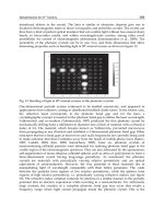
sputtering system in our experiments is shown in Figure 7. Figure 8 shows a photograph of
the typical glow from ZnO target when sputtering.
As-doped ZnO films were grown on glass and SiO2/Si substrates at different substrate
temperatures by sputtering Zn3As2/ZnO or cosputtering ZnO and Zn3As2 targets. Undoped
ZnO films were deposited by sputtering ZnO target. Silicon oxide layer with a thickness of
250 nm was thermally grown in dry oxygen on Si substrate. The substrates were first
cleaned by acetone and ethanol and then rinsed in de-ionized water each for 5 min at room
temperature. The sputtering chamber was evacuated to a base pressure of 10-3Pa. A pure Ar
(99.999%) was used as the working gas. The distance between the targets and the substrate
was 14cm. The targets were presputtered for 20 min to remove contaminants. The As-doped
ZnO targets were prepared by adding Zn3As2 and sintering at 9000C for 3h. The Zn3As2
contents in the targets were 0.5mol%, 1.0mol%,1.5mol%,2mol%, respectively. The pure
Zn3As2 target was sintered in pure Ar (purity: 99.999%; pressure: 0.1MPa) at 8000C for 2h.
The film thickness was measured with ellipsometer.
Fabrication and Characterization of As Doped p-Type ZnO Films Grown by Magnetron Sputtering
399
Fig. 7. Schematic diagram of the magnetron sputtering system.
Fig. 8. Photograph of the typical glow from ZnO target when sputtering.
The structures and morphologies of the as-grown ZnO films were characterized by X-ray
diffraction (XRD, Siemens D-5000, and Cu Ka, λ = 1.5405Å), atomic force microscopy
(AFM, NTD-Pro47) and scan electron microscopy (SEM, JSM-6700F). The composition of
As-doped ZnO film was analyzed by an energy dispersive X-ray (EDX) spectroscopy
(INCA, Oxford) attached to the SEM. The concentration of As in ZnO film was measured
with Secondary ion mass spectroscopy (SIMS, Physical Electronicsmodel 7200). The
bonding state of As in ZnO:As films were studied by x-ray photoelectron spectroscopy
(XPS) using the Mg Kα line (Physical Electronics model5600). The x-ray source and the C
1s line were taken as the standard reference. The electrical properties of the films were
investigated at room temperature in the Van der Pauw configuration using HL5500 Hall
system. The measurement process was the following: ensuring Ohmic contact→the
resistivity measurement→Hall effect measurement→repeating Hall effect measurement.
During the whole measurement, the resistivity was measured once and every sample had
one value of the resistivity and several values of the mobility and carrier concentration.
For one sample, if the results of several Hall effect measurements showed the same
400
Optoelectronics - Materials and Techniques
conduction type, we consider it had stable conduction type. If the results of several Hall
effect measurements were not consistent, and the conduction type of the film was not
confirmed. The optical transmission spectra of the films were measured at room
temperature using an UV–vis double beam spectrometer. Low temperature
photoluminescence (PL) were systematically performed for ZnO films by the excitation
from 325 nm He-Cd laser.
5. Results and discussion
5.1 Undoped ZnO films
First, let us investigate the properties of undoped ZnO films grown by magnetron
sputtering. The undoped ZnO films were deposited on glass substrates at various
temperatures from 250 to 4500C with RF power of 120W. High purity Ar (99.999%) or
mixture of Ar and O2 (Ar:O2 = 3:1) maintained at 0.6 Pa was used as the working gas. In
addition, the ZnO film measured low temperature PL was prepared on SiO2/Si substrate at
3500C with purity Ar maintained at 0.5 Pa.
Figure 9 shows the XRD patterns of ZnO powder and film deposited at 4500C.
Fig. 9. XRD patterns of ZnO powder (a) and film deposited at 4500C (b).
Many diffraction peaks, such as (100), (002), (101) were seen in the pattern of ZnO powder
and the (002) peak was not the strongest one. In the pattern of ZnO film deposited at 4500C,
a strong peak of (002) at about 34.50 and a weak peak of (004) at 72.60 were observed.
Comparison of the patterns shows that the thin film tended to be oriented on the (001)
surface. SEM photograph in Figure 5 showed that the grains of ZnO film were small, around
100nm in diameter, in which exhibited hexagonal form and the powder were composed of
ZnO grains with different diameters.
The optical absorption spectra of ZnO powder and film deposited at 4500C in the visible are
displayed in Figure 10. The fundamental absorption for both powder and film starts from
about 370 nm and the absorption of film in UV region was stronger, obviously. The inset
shows a plot of (αhν)2 against hν for ZnO film and the optical band gap (Eg) value was
obtained by extrapolating the linear portion to photo energy axis. It was found to be about
3.262eV.
Fabrication and Characterization of As Doped p-Type ZnO Films Grown by Magnetron Sputtering
401
Fig. 10. Absorption spectra of ZnO powder (b) and film (a).The film thickness was about
300 nm. Inset shows plot of (ahv)2 against hv for estimation of direct allowed optical gap of
the film. The estimated gap was 3.262eV.
Figure 11 shows XRD patterns of ZnO films grown with different conditions. The growth
parameters of the films were summarized in Table 2. A strong peak of ZnO (002) at about
34.50 was observed for each sample, indicating that the films were c-axis oriented. The fullwidth at half-maximum (FWHM) of (002) peaks were listed in Table 2. (103) peak in the
XRD pattern of the film grown at 2500C (SampleSA) shows that c-axis oriented grains in the
film did mot dominate completely due to the low growth temperature. (103) peak
disappeared in the films deposited at 3500C (SampleSB), indicating the c-axis orientation of
the film became stronger and the crystallinity was improved, which was consist with the
change of (002) FWHM from 0.400 to 0.380. Comparison of the patterns of SamleSB, SC and
SB+annealing shows that the induction of O2 in working gas and post-annealed improved
the quality of ZnO films grown with magnetron sputtering.
Fig. 11. XRD patterns of ZnO films grown different conditions: (a) PAr =0.6Pa, 2500C; (b) PAr
=0.6Pa, 3500C; (c) PAr =0.45Pa, PO2 =0.15Pa, 3500C.
402
Optoelectronics - Materials and Techniques
Table 2. Growth parameters and (002) FWHM of ZnO films.
Fig. 12. XRD patterns of as-grown ZnO film at 3500C and annealed at 450 0C in air for 2h.
The surface morphologies of ZnO films were investigated by AFM. Figure 13 shows AFM
images of ZnO films grown with different conditions. It can be seen that the grains of the
films became larger with the temperature increased from 250 to 3500C and post-annealing
improved the uniform of the film, which indicated the crystallinity of the films improved
and were consisted with the results of XRD.
Figure 14 shows the optical transmittance spectra of ZnO films. The transmittances are over
70% in the visible region for all the films and the fundamental absorptions are at about
370nm. The inset of Figure 14 reveals the relationship between absorption coefficient and
photo energy of ZnO film deposited at 3500C. The Eg value estimated was 3.271 eV.
Low temperature PL was performed for ZnO film grown on SiO2/Si substrate. The near band
edge (NBE) part of the 10 K PL spectrum was shown in Figure 15, which had peaks at 3.355,
3.308, and 3.234eV (Fan, et al., 2009). Similar lines were also observed by Petersen et al., (3.350
and 3.303eV) in n-type ZnO grown by sol-gel process (Petersen, et al., 2008 )and by Zhong et al
(3.357 and 3.309eV) in ZnO tetrapod(Zhong, et al., 2008). The ~3.36 eV was ascribed to the
neutral donor-bound-exciton (D0X) according to D.C.Look 's suggestion about the peak (Look
& Clalin,2004). The 3.31 eV line was associated with the corresponding two-electron-satellite
(TES) and/or exciton-LO phonon emission, therefore, the peaks at 3.355 and 3.308eV in Figure
15 were assigned to be the D0X and the TES/exciton-LO phonon lines, respectively. The 3.234
eV observed in Figure 15 was similar to the ~3.24eV donor-acceptor-pair (DAP) emission
suggested by Peterson et al (Petersen, et al., 2008), and were thus assigned as DAP.
Fabrication and Characterization of As Doped p-Type ZnO Films Grown by Magnetron Sputtering
(a)
403
(b)
(c)
Fig. 13. AFM images of ZnO films prepared with different conditions:(a) PAr =0.6Pa, 2500C;
(b) PAr =0.6Pa, 3500C; (c) SB+annealing.
Fig. 14. Transmittance spectra of as-grown ZnO films prepared with different conditions: (a)
PAr =0.6Pa, Room temperature; (b) PAr =0.6Pa, 2500C; (c)PAr =0.6Pa, 3500C; The inset is the
(αhν)2 vs hν curve for the optical band gap determination in the filmdeposited at 3500C. The
Eg value estimated was 3.271eV.