Solar Cells Silicon Wafer Based Technologies Part 3 ppt
Bạn đang xem bản rút gọn của tài liệu. Xem và tải ngay bản đầy đủ của tài liệu tại đây (352.02 KB, 25 trang )
Epitaxial Silicon Solar Cells
41
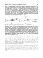
specific boundary conditions when the device is operated under short circuit, concerning
the grain boundary recombination velocity in the active layer S
ng
and the effective back
surface recombination velocity S
eff
at the low / high junction. The simplified relation gives
the expression for effective electron recombination velocity S
eff
, as a function of the
material’s doping concentration of the active layer and the substrate (Ν
Α
, Ν
Α
+
), assumed
constant all over of these regions’ bulk (Eq.7). Moreover the grain boundary recombination
velocity in the front and the active layer is considered the same and symbolized as S
gb
.
The solution of the continuity equations (14) and (16) is obtained in analytical form using the
Green’s function method. This procedure is briefly described in (kotsovos. K & Perraki. V;
2005). The analytical expression of the front layer photocurrent density J
p
is derived, by
differentiating the hole density distribution in the junction edge region z=d
1
-w
n
presented in
the form of infinite series (Halder. N.C, & Williams. T. R., 1983):
22
22
,
(,,) 4
sin( )sin( )
cos( )cos( )
(1)
p
peff x y g g
mn
peff
Jxy qF
LMN mX nY
mx ny
mn L
11
1
1
11
exp( ( )){ cosh( ) sinh( )}
[ exp( ( ))]
sinh( ) cosh( )
nn
ppeff np
peff peff
peff n
nn
p
peff peff
dw dw
NL dwN
LL
Ldw
dw dw
N
LL
(17)
where the variables x and y represent arbitrary points inside the grain and M
x
, N
y
, L
peff,
N
p
are expressed by proper equations as functions of S
pg
,D
p
, X
g
, Y
g
, L
p
, and S
F.
In a similar way the analytical expression of the base region photocurrent density J
n
is given,
in the form of infinite series, by differentiating the electron density distribution in the
junction edge region z=d
2
–w
p
by the relation
1
()
22
22
,
4
sin( )sin( )
cos( )cos( )
(1)
p
dw
n
neff x y g g
kl
neff
JqFe
LKL kX lY
kx ly
kl L
22
() ()
22
22
{cosh( ) ) sinh( )} )
[]
sinh( ) cosh( )
pp
dw dw
pp
nneff
neff neff
neff
pp
n
neff neff
dw dw
Ne Le
LL
L
dw dw
N
LL
(18)
Where K
x
, L
y
, L
neff,
N
n
are expressed as functions of S
eff
, S
ng
,D
n
, X
g
, Y
g
, L
n.
The photogenerated current in the Space Charge Region (equal to the number of photons
absorbed), is derived by the 1D model (Sze. S. M, 1981):
1
()
()
{1 }
np
n
ww
dw
SCR
JqFe e
(19)
Solar Cells – Silicon Wafer-Based Technologies
42
The total photocurrent is given from the sum of all current densities in each region
considering as it has been early referred (Dugas. J.& Qualid. J, 1985) that the substrate
contribution is negligible:
sc
p
nSCR
JJJJ
(20)
A similar analysis might also carried out, for the determination of the dark saturation
current (
J
0
) by solving the continuity equations, for both regions, (Halder. N. C, & Williams.
T. R., 1983). The derived expression of
J
0
is then used for the calculation of open circuit
voltage from Eq 13.
4. Optimization
A computer program has been developed according to the mathematical analysis which
implements the 1D model previously described (3.1) for the optimization of cells
parameters. The values of ref1ection coefficient R(λ) which depends on the wavelength λ
and is related to the anti reflecting coating, as well as the photon flux Ν (λ) defined by a
discretized AM1.5 solar spectrum, are inserted in the program via the modelling procedure.
The grid structure of the cell covering about 13.1% of the front surface and the Back Surface
Field are inserted in a similar way. Material properties are considered as previously
described, however the required data must be inserted by the user manually e.g., data
concerning front layer and substrate (thickness, doping concentration), concentration of the
front layer N
D
, front surface recombination velocity S
F
and effective recombination velocity
S
eff
, e.t.c. This data is then used as the starting point for the optimisation process. The
program calculates the external quantum efficiency of the studied cells in a wavelength
range from 0.4μm to 1.1μm, under 1000 W/m
2
illumination (AM1.5 spectrum). The
optimisation is carried out by introducing the lower and upper bounds of the epilayer
thickness which are 40 and 100 μm respectively (Perraki. V & Giannakopoulos. A.; 2005).
The simulation is then performed in batch mode with respect to the input data, controlling
the input and output of the simulator at the same time.
After completion of this operation, results are interpreted and assessed by the output
interface. The simulated short circuit current density is initially evaluated through
numerical integration for the corresponding spectrum, while efficiency of the cells is
investigated in the next step.
A 3D model is applied (3.2) to the same type of cells in order to optimize their epitaxial layer
thickness, taking into account the structure parameters. The program computes the external
quantum efficiency of the studied cells. It also provides, through numerical integration,
results for the optimum photocurrent density and efficiency for various values of grain size
and grain boundary recombination velocity.
A comparison between the 3D simulated and experimental results of photocurrent, and
efficiency under AM1.5 irradiance is performed, as well as between the quantum efficiency
curves calculated through 3D model and the corresponding 1D results of the studied cells.
5. Influence of structure parameters on cell’s properties
The simulations for n
+
pp
+
type epitaxial silicon solar cells, have been performed under AM
1.5 spectral conditions. The experimental values, of emitter (thickness d
1
, diffusion length L
P
Epitaxial Silicon Solar Cells
43
and doping concentration N
D
), and substrate (thickness d
3
, diffusion length L
n
+
and doping
concentration N
A
+
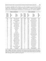
), assigned to the model parameters are shown in Table 3.
Cell d
1
(μm) L
p
(μm) N
D
(cm
-3
) d
3
(μm) L
n
+
(μm) N
A
+
(cm
-3
)
B2 0.4 1 1.5x10
20
300 13 2.9x10
19
T2 0.4 1 1.5x10
20
300 18 1.9 x10
19
Table 3. Experimental values of emitter and substrate characteristics.
The experimental values of epilayer properties (thickness d
2
, base doping concentration N
A
,
diffusion length L
n
) and the best results of measured photocurrent density J
sc
, open circuit
voltage V
oc
and efficiency η for the cells under investigation are shown in table 4.
Cell d
2
(μm) N
A
(cm
-3
) L
n
(μm) J
p
h
(mA/cm
2
) V
oc
(V) η (%)
B2 64 1.5x10
16
64 25.05 542 9.3
T2 64 1.5x10
16
71 26.17 558 10.12
Table 4. Experimental values of epilayer properties.
5.1 One dimensional model
The one dimensional model was utilized to perform simulations that indicate the
dependency of cell’s photovoltaic properties on recombination velocity and doping level,
for the cells (B2, from the bottom of the ingot) as well as for cells (T2, from the top of the
ingot). Optimal photocurrent density and efficiency are calculated as a function of epilayer
thickness for two different values of recombination velocity, and two different values of
doping concentration.
5.1.1 Influence of recombination velocity
Figure 3 shows that the photocurrent density is little influenced (Hoeymissen,J. V; et al 2008)
in cases of low recombination velocity (10
2
cm/sec). On the contrary photocurrent density is
heavily affected by the epilayer thickness in case of high recombination velocity (10
6
cm/sec) and a value ~30 mA /cm
2
is achieved for epilayer thickness values much higher
than 65 μm. The evaluation of these results shows that the epilayer thickness of 50 μm
represents a second best value, in case of low recombination velocity. The gain, for thicker
epilayers than this, is minor with an increment in J
sc
of approximately ~ 0.05 mA /cm
2
,
when the epilayer thickness increases by steps of 5 μm.
The plots of the efficiency with respect to epilayer thickness for two different values of
recombination velocity are illustrated in figure 4.
It is observed that the efficiency of the studied cells, calculated for recombination velocity
values of 100 cm/sec saturates (η~13.8%) for epilayer thickness values higher than ~65μm
where the gain is minimal. However for recombination velocity values of 2.5x10
6
cm/sec the
efficiency is lower enough for thin epilayers and saturates for thickness values higher than
85μm. Higher efficiencies are referred to cells with small grains, in comparison to those of
large grains, because of the presence of fewer recombination centres. Annotating these results
it is found that when the epilayer thickness of these cells decreases to values ≤ 50 μm the
maximum theoretical efficiency decreases by a percentage of 0.03 % to 0.07 % for S
eff
=100 cm/
sec. It is particularly recommended that a second best value of epilayer thickness equals to 50
μm, given that the gain for higher epilayer thickness values is of minor importance.
Solar Cells – Silicon Wafer-Based Technologies
44
24
25
26
27
28
29
30
31
40
50
60
70
80
90
100
Epilayer thickness d2 (μm)
Jsc(mA/cm
2
)
B2,100 T2,100
B2,2.5*10^6 T2,2.5*10^6
Fig. 3. Variation of short circuit current density, J
sc
, of the studied cells (B2 with small grains,
T2 with large grains) versus epilayer thickness d2, calculated for S
eff
=100 cm/sec and 2.5x10
6
cm/sec.
11,5
12
12,5
13
13,5
14
40 50 60 70 80 90 100
Epilayer thickness d2 (μm)
η(%)
B2,100 B2,2.5x10^6
T2,100 T2,2.5x10^6
Fig. 4. Efficiency graph versus base thickness d2 of the cells under investigation, calculated
for S
eff
=100 cm/ sec and 2.5x10^6 cm/sec.
5.1.2 Influence of doping concentration
The same model was used to perform simulations indicating the relation between
photovoltaic properties and doping concentration. When doping concentration increased
from 10
15
to 10
17
cm
-3
simulated data of the short circuit current density, J
sc,
showed a small
decrease, due to Auger recombination and minority charge carriers’ mobility.
Figure 5, illustrates the variation of J
sc
with respect to epilayer thickness for two different
values of doping. Maximum photocurrent densities are delivered from cells with epilayer
thickness equal to 65 and 70 μm (B2 and T2 cells respectively). They vary between 29.6 and
Epitaxial Silicon Solar Cells
45
29
29,5
30
30,5
4
0
5
0
6
0
7
0
8
0
9
0
1
0
0
Epilayer thickness d2 (μm)
Jsc(mA/cm
2
)
B2,10^15 B2,10^17
T2,10^15 T2,10^17
Fig. 5. Variation of the short circuit current density J
sc
of the cells, as a function of base
thickness d2 calculated for doping concentration values of 10
15
cm
-3
,
and 10
17
cm
-3
.
30.47 mA /cm
2
, which are higher than experimental values. According to the calculated
results when the epilayer thickness of B2 cells decreases to values ≤50 μm, photocurrent
density decreases for the different values of doping concentrations by approximately 0.05-
0.08 mA/cm
2
. It can be considered again that 50 μm, represent a second best value, since
little is gained when the epitaxial layer becomes thicker.
Simulated data of cell efficiency, η, present a rise of its maximum value, as shown in figure
6, which is well above from maximum values experimentally obtained, and a shift of the
optimum epilayer thickness to lower values. Higher efficiency has been calculated for cells
with doping concentration of 10
17
cm
-3
compared to the one calculated for cells with doping
11,7
12,2
12,7
13,2
13,7
14,2
14,7
15,2
4
0
5
0
6
0
7
0
8
0
9
0
1
0
0
Epilayer thickness d2(μm)
η %(%)
B2,10^15
B2,10^17
T2,10^15
T2,10^17
Fig. 6. Variation of the cell’s efficiency as a function of epilayer thickness d2 calculated for
doping concentrations of 10
15
cm
-3
,
and 10
17
cm
-3
.
Solar Cells – Silicon Wafer-Based Technologies
46
of 10
15
cm
-3
. It is noticed that solar cell efficiency is insignificantly influenced by epilayer
thickness variations. It is pointed that if the epilayer thickness of the small grain cell is
reduced to values ≤50 μm, the efficiency decrease is less than 0.03%. Similarly a decrease in
epilayer thickness, of T2 cells, to 50 μm results in a decrease of their maximum efficiency by
0.04 %.
The optimized cell parameters J
sc
and η for an optimum value of doping concentration show
that even they are higher compared to the experimental ones, (Perraki. V.; 2010) they do not
present significant differences for the two different types of cells. This is due to the fact that
cell parameters introduced to the model were not very different and diffusion length values
were high in all cases. It must be noted however that the optimum values of photocurrent
density, efficiency and epilayer thickness calculated by this model are different than the
ones corresponding to maximum J
ph
and η and equal the values of saturation. When the
epilayer thickness increases beyond the optimum value in steps of 5 μm, J
sc
and η increase
by a rate lower than 0.05mA/cm
2
and 0.05% respectively. Taking all these into account, we
can consider that the optimum value of efficiency is obtained for epilayer thickness values
equal to or lower than 50 μm, which is much lower than base thickness and base diffusion
length values of any solar cell.
The comparison between the experimental and the optimized quantum efficiency plots of B2
and T2 cells, (calculated by the 1D model) is presented in figure 7. The chosen model
parameters, as shown in tables 3 and 4, provide a good fit to the measured QE data for
wavelength values above 0.8 μm, whereas optimized curves indicate higher response for the
lower part of the spectrum. The response of the experimental devices related to the
contribution of the n
+
heavily doped front region (for low wavelengths of the solar
radiation) is significantly lower than that of the simulated results, due to the non passivated
surface.
Moreover, the spectral response of B2 is significantly higher compared to the one of T2 cell
near the blue part of the solar spectrum, although cell T2 has higher experimental values of
J
sc
, V
oc
, and η. This may be explained by differences of the reflection coefficient between
experimental and simulated devices and /or by the presence of fewer recombination centers
in smaller inter-grain surfaces.
0
20
40
60
80
100
0,4 0,56 0,72 0,88 1,04
Wavelenght λ(μm)
QE(%)
B2opt T2opt
B2exp T2exp
Fig. 7. Optimized external quantum efficiency for cells B2, and T2, evaluated for
experimental values included in tables 3 and 4, and comparison with the experimental ones.
Epitaxial Silicon Solar Cells
47
5.2 Three dimensional model
A 3D model was utilized to perform simulations that show the influence of grain boundary
recombination velocity S
gb
and grain size on cell’s properties. The calculated results indicate
the influence of grain boundary recombination velocity on the photocurrent and on the
efficiency for various values of grain size for the cells B2 (from the bottom of the ingot) as
well as for the cells T2 (from the top of the ingot). The plots are obtained for values of
epilayer thickness maximizing the photocurrent which are not necessarily equal to the
experimental. These optimal values of epilayer thickness used in the graph vary and depend
on grain size and S
gb
The graph of optimal photocurrent as a function of recombination velocity shows, figure 8,
that it is seriously affected by recombinations in the grain boundaries of small grains, given
that a significant amount of the photogenerated carriers recombine in the grain boundaries
when grain’s size is lower or comparable to the base diffusion length.
8
10
12
14
16
18
20
22
24
26
28
10^2 10^3 10^4 10^5 10^6
S
gb
(cm/sec)
Jsc (mA/cm
2
)
grain 10μm
grain100μm
grain500μm
Fig. 8.
Optimal short circuit current dependence on grain boundary recombination velocity
S
gb
of the cell B2, with grain size as parameter.
It is shown that the photocurrent density falls rapidly for grains with size 10 μm and high
values of grain boundary recombination velocities. However, the effect of grain boundary
recombination velocity is not so important for larger grain sizes (100 and 500 μm).
Figure 9 demonstrates the efficiency of the cells B2 in relation with the grain boundary
recombination velocity for different grain sizes, which is
calculated for optimal base
thickness. It can be pointed that for small grain size, the efficiency is largely affected by
grain boundary recombination, with a rapid decrease for recombination velocities greater
than 10
3
cm/sec.
For larger grain sizes (500 μm), there is not so strong decrease with the recombination
velocity, while insignificant decrease is observed in the efficiency for values lower than 10
3
cm/sec.
The graphs of optimal photocurrent as a function of grain boundary recombination velocity
(figure 10) show that it is less affected from recombination in the grain boundaries for large
grain sizes (cells T2), compared to cells with small grain sizes, (cells B2 in figure 8).
Solar Cells – Silicon Wafer-Based Technologies
48
4
2.004
4.004
6.004
8.004
10.004
12.004
14.004
10^2 10^3 10^4 10^5 10^6
S
gb
(cm/sec)
Efficiency η(%)
grain 10μm
grain100μm
grain500μm
Fig. 9.
Variation of efficiency η of the cell B2, as a function of grain boundary recombination
velocity S
gb
, calculated for optimal base thickness and variable grain sizes.
Therefore, for grains with size 5000 μm, and high values of grain boundary recombination
velocities the photocurrent does not fall rapidly. It is evident that, for cells with even larger
grain sizes (10000 μm) the influence of grain boundary recombination velocity is even more
insignificant.
25,8
25,85
25,9
25,95
26
26,05
26,1
26,15
26,2
26,25
26,3
10^2 10^3 10^4 10^5
S
gb
(cm/sec)
Jsc (mA/cm
2
)
grain5000μm
grain10000μm
Fig. 10. Optimal short circuit current dependence on grain boundary recombination velocity
S
gb
of the cell T2, with grain size as parameter.
Epitaxial Silicon Solar Cells
49
12.200
12.250
12.300
12.350
12.400
12.450
10^2 10^3 10^4 10^5
Sgb (cm/sec)
Efficiency η(%)
grain5000μm
grain 10000μm
Fig. 11.
Variation of the efficiency η as a function of grain boundary recombination velocity
S
gb
, calculated for optimal base thickness and variable grain sizes (cell T2).
(a) (b)
Fig. 12. Optimized external quantum efficiency and comparison with 3D model, for the cells
B2 (a) and T2 (b), evaluated for experimental values included in tables 3 and 4.
Figure 11 illustrates the efficiency of the cells T2 as a function of grain boundary
recombination velocity for different grain sizes, which is
calculated for optimal base
thickness. It can be observed that for large grain size, (5000 μm) the efficiency is less affected
for grain boundary recombination for S
gb
values higher than 10
3
cm/sec, compared to the
case of small grain size, Fig. 9. A smoother decrease is observed in case of cells with even
Solar Cells – Silicon Wafer-Based Technologies
50
larger grain sizes (10000 μm). It is obvious that solar cell efficiency saturates if S
gb
is lower
than 10
3
cm/sec and the gain is minimal for smaller values of grain boundary recombination
velocity. In this case, efficiency is limited from bulk recombination, which is directly related
to the base effective diffusion length L
n
. However when grain boundary recombination
velocity is reduced, the optimal layer thickness increases, until it reaches a value close to the
device diffusion length L
n
.This parameter seems to affect the value of optimal epilayer
thickness. For higher S
gb
values the maximum efficiency shifts to thickness values lower
than the base diffusion length. However, for very elevated values of grain boundary
recombination velocities and small grain size, the optimal thickness saturates to a value,
which is the same for cells with thin or thick epilayer. The plots of L
neff
and optimal epilayer
thickness as a function of S
gb
, show similar dependence on S
gb
and grain size, with almost
equal values (Kotsovos. K & Perraki.V, 2005).
The optimized 1D external quantum efficiency and the 3D graphs are demonstrated for the
cells B2 and T2 in figure 12a and b respectively (kotsovos. K, 1996). Since the influence of
grain boundaries has not been taken into account in the 1D model it has shown superior
response compared to the 3D equivalent for wavelength values higher than 0.6 μm (cell T2).
Lower values of spectral response are observed in case of large grains (cell T2) and λ> 0.6
μm, possible due to the presence of more recombination centers in larger intergrain surfaces.
However, very good accordance is observed between 1D and 3D plots for cells B2.
6. Conclusions
The optimal photocurrent and conversion efficiency for epitaxial solar cells are influenced
by the recombination velocity. The best values of epilayer thickness and the effective base
diffusion length are higher for lower values of grain boundary recombination velocities,
resulting to higher efficiency values.
The comparison between the simulated 1D and experimental QE curves indicates
concurrence for wavelengths greater than 0.8 μm. However, the measured spectral response
close to the blue part of the spectrum was considerable lower compared to simulation data.
On the other hand the comparison of the simulated 1D and 3D QE curves shows good
agreement only for wavelengths lower than 0.6 μm for cells T2 and very good agreement for
cells B2.
7. References
Arora. J, Singh. S, and Mathur. P., (1981), Solid State Electronics, 24 (1981), p.739-747.
Blacker. A. W, et al (1989)
Proc. 9
th
EUPVSEC, Freiburg, Germany, p.328.
Card. H.C, and Yang. E., (1977),
IEEE Trans. Electron Devices, 29 (1977) 397.
Carslaw. H.S; and Jaeger .J.C; 1959;
Conduction Heat in Solids, 2
nd
ed, Oxford University
Press, London 1959.
Caymax. M; Perraki. V; Pastol.J. L; Bourée. J.E; Eycmans. M; Mertens. R; Revel. G; Rodot. M;
(1986)“resent results on epitaxial solar cells made from metallurgical grade Si”
Proc.2
nd
Int.PVSE Conf (Beijing1986)171.
Epitaxial Silicon Solar Cells
51
Duerinckh. F; Nieuwenhuysen. K.V; Kim. H; Kuzma-Filipek. I; Dekkers. H; Beaucarne. G;
and Poortmans. J; (2005) “Large –area Epitaxial Silicon Solar Cells Based on
Industrial Screen-printing Processes”
Progress in Photovoltaics 2005,pp673
Dugas.J, and Qualid. J, (1985), “3d modelling of grain size and doping concentration
influence on polycrystalline silicon solar cells”,
6
th
ECPVSEC, (1985) p. 79.
Godlewski. M; Baraona.C.R and Brandhorst.H.W 1973,
Proc 10
th
IEEE PV Specialist Conf.
(1973) P.40
Goetzberger.A, Knobloch. J, Voss. B;
Crystalline Silicon Solar Cells, John willey & Sons 1998.
Halder. N.C, and Williams. T. R., (1983);“Grain Boundary Effects in Polycrystalline Silicon
Solar Cells”,
Solar Cells 8 (1983) 201.
Heavens. O. S, (1991);
The Optical Properties of Thin solid Films, Dover, 1991.
Hoeymissen. J.Van; Kuzma-Filipek. I; Nieuwenhuysen. K. Van; Duerinckh. F; Beaucarne. G;
J. Poortmans. J; (2008) “ Tnin-film epitaxial solar cells on low cost Si substrates:
closing the efficiency gap with bulk Si cells using advanced photonic structures and
emitters”,
Proceedings 23
rd
EUPVSEC 2008 pp 2037.
Hovel. H. J. (1975) Solar cells
Semiconductors and Semimetals vol. II (New York: Academic
Kotsovos. K; 1996,
Final year student Thesis, University of Patras,Greece,1996
Kotsovos. K and Perraki.V; (2005) “Structure optimisation according to a 3D model applied
on epitaxial silicon solar cells :A comparative study
” Solar Energy Materials and Solar
Cells
89 (2005) 113-127.
Luque. A, Hegeduw. S.,(ed) “
Handbook photovoltaic Science and Engineering ‘’ Wiley, 2003.
Mason. N; Schultz. O; Russel. R; Glunz. S.W; Warta. W; (2006) “20.1% Efficient Large
Area Cell on 140 micron thin silicon wafer”,
Proc. 21
st
EUPVSEC, Dresden 2006, pp
521
Nieuwenhuysen. K. Van; Duerinckh. F; Kuzma. I; Gestel. D.V; Beaucarne. G; Poortmans. J;
(2006) ” Progress in epitaxial deposition on low-cost substrates for thin- film
crystalline silicon solar cells at IMEC”
Journal of Crystal Growth (2006) pp 438
Nieuwenhuysen. K.Van; Duerinckx. K; Kuzma. F; Payo. I; Beaucarne. M.R; Poortmans. G;
(2008); Epitaxially grown emitters for thin film crystalline silicon solar cells
Thin
Solid Film
, 517, (2008) pp 383-384.
Overstraeten. R.J.V, Mertens. R, (1986),
Physics Technology and Use of Photovoltaics, Adam
Hilger Ltd 1986.
Perraki. V and Giannakopoulos.A; (2005); Numerical simulation and optimization of
epitaxial solar cells;
Proceedings 20th EPVSEC Barcelona 2005, pp1279.
Perraki.V; (2010) “Modeling of recombination velocity and doping influence in epitaxial
silicon solar cells”
Solar Energy Materials & Solar Cells 94 (2010) 1597-1603.
Peter.K; Kopecer.R; Fath. P; Bucher. E; Zahedi. C;
Sol. Energy Mat. Sol. Cells 74 (2002) pp 219.
Peter. K; R.Kopecek. R; Soiland. A; Enebakk. E; (2008) ″Future potential for SOG-Si
Feedstock from the metallurgical process route″
Proc.23
rd
EUPVSEC (2008) pp 947
Photovoltaic Technology Platform; (2007) “A Strategic Research Agenda for PV Energy
Technology”;
European Communities, 2007
Price J.B.,
Semiconductor Silicon, Princeton, NJ, 1983, p. 339
Runyan. W. R, (1976)
Southeastern Methodist University Report 83 -13 (1976).
Solar Cells – Silicon Wafer-Based Technologies
52
Sanchez-Friera. P;et al;(2006)“Epitaxial Solar Cells Over Upgraded Metallurgical Silicon
Substrates: The Epimetsi Project”
IEEE 4
th
World Conference on Photovoltaic Energy
Conversion
, pp1548-1551.
Sze. S. M;
Physics of Semiconductor Devices, 2nd Ed, 1981, p 802
Wolf H. F.,
Silicon Semiconductor Data, Pergamon Press, 1976.
3
A New Model for Extracting the Physical
Parameters from I-V Curves of Organic
and Inorganic Solar Cells
N. Nehaoua, Y. Chergui and D. E. Mekki
Physics Department, LESIMS laboratory,
Badji Mokhtar University
Algeria
1. Introduction
As worldwide energy demand increases, conventional sources of energy, fossils fuels such
as coal, petroleum and natural gas will be exhausted in the near future. Therefore,
renewable resources will have to play a significant role in the world’s future supply. Solar
energy occupies one of the most important places among these various possible alternative
energy sources. The direct photovoltaic conversion of sunlight into electricity seems to be
extremely promising. Solar cells furnish the most important long-duration power supply for
satellites and space vehicles. They have also been successfully employed in terrestrial
application. A solar cell (also called photovoltaic cell or photoelectric cell) is a solid state
device that converts the energy of sunlight directly into electricity by the photovoltaic effect.
Assemblies of cells are used to make solar modules, also known as solar panels. The energy
generated from these solar modules, referred to as solar power, is an example of solar
energy. photovoltaic system uses various materials and technologies such as crystalline
Silicon (c-Si), Cadmium telluride (CdTe), Gallium arsenide (GaAs), chalcopyrite films of
Copper-Indium-Selenide (CuInSe2) and Organic materials are attractive because of their
light eight, processability, and the ease of designing the materials on the molecular level.
Solar cells are usually assessed by measuring the current voltage characteristics of the device
under standard condition of illumination and then extracting a set of parameters from the
data. The major parameters are usually the diode saturation current, the series resistance,
the ideality factor, the photocurrent and the shunt conduction. The extraction and
interpretation has a variety of important application. These parameters can, for instance, be
used for quality control during production or to provide insights into the operation of the
devices, thereby leading to improvements in devices.
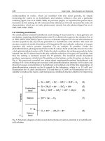
2. Equivalent circuit of solar cells
A solar cell is simply diode of large-area forward bias with a photovoltage. The
photovoltage is created from the dissociation of electron-hole pairs created by incident
photons within the built-in field of the junction or diode. The operating current of a solar
cell is given by:
Solar Cells – Silicon Wafer-Based Technologies
54
exp 1
ph d p
s
ph s s
sh
II I I
VIR
II VIR
nR
(1)
Where, I
ph
, I
s
, n, R
s
and G
sh
(=1/R
sh
) being the photocurrent, the diode saturation current,
the diode quality factor, the series resistance and the shunt conductance, respectively. I
p
is
the shunt current and β=q/kT is the usual inverse thermal voltage. The shunt resistance is
considered R
sh
= (1/G
sh
)>>Rs.
The circuit model of solar cell corresponding to equation (1) is presented in figure (1).
Fig. 1. Equivalent circuit model of the illuminated solar cell.
The single diode model considered here is rather simple, efficient and sufficiently accurate
for process optimization and system design tasks. The single diode model can also be used
to fit solar modules and arrays where the cells are series and/or parallel connected,
provided that the cell to cell variations are not important.
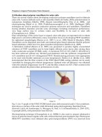
3. Solar cell output parameters
The graph of current as a function of voltage I=f (V) for a solar cell passes through three
significant points as illustrated in figure 2 below.
- The short circuit current, I
sc
, occurs on a point of the curve where the voltage is zero. At
this point, the power output of the solar cell is zero. The current in a device is almost
directly proportional to light intensity and size.
- The open circuit voltage, V
oc
, occurs on a point of the curve where the current is zero.
At this point the power output of the solar cell is zero. The voltage of the cell does not
depend on its size, and remains fairly constant with changing light intensity.
- The fill factor, FF, is the ration of the peak power to the product I
sc
V
oc
oc
mm
scV
IV
FF
I
(2)
A New Model for Extracting the
Physical Parameters from I-V Curves of Organic and Inorganic Solar Cells
55
The fill factor determines the shape of the solar cell I-V characteristics. Its value is
higher than 0.7 for good cells. The series and shunt resistance account for a decrease in
the fill factor. The fill factor is useful parameters for quality control test.
- The conversion efficiency, is the ration of the optimal electric power, P
m
, delivered by
the PV module to the solar insolation, P
0
, received at a given cell temperature, T.
00
sc oc m
FF I V P
PP
(3)
Fig. 2. Solar cell I-V Characteristics.
4. Solar cell parameters extraction
4.1 Previous works
An accurate knowledge of solar cell parameters from experimental data is of vital
importance for the design of solar cells and for the estimates of their performance. The major
parameters are usually the diode saturation current, the series resistance, the ideality factor,
the photocurrent and the shunt conductance.
The evaluation of these parameters has been the subject of investigation of several authors.
Some of the methods use selected parts of the current-voltage (I-V) characteristic (Charles et
al, 1981; 1985) and those that exploit the whole characteristic (Easwarakhanthan et al, 1986;
phang et al, 1986). (Santakrus et al, 2009) presents the use of properties of special trans
function theory (STFT) for determining the ideality factor of real solar cell. (Priyank et al,
2007) method gives the value of series R
s
and shunt resistance R
sh
using illuminated I-V
characteristics in third and fourth quadrants and the V
oc
-I
sc
characteristics of the cell. In the
work of (Bashahu et al, 2007), up to 22 methods for the determination of solar cell ideality
factor (n), have been presented, most of them use the single I-V data set. (Ortiz-Conde et al,
Solar Cells – Silicon Wafer-Based Technologies
56
2006) have proposed an elegant method to extract the five parameters based on the
calculation of the co-content function (CC) from the exact explicit analytical solution of the
illuminated current–voltage characteristics, but this method has only been tested on a plastic
solar cell. An accurate method using the Lambert W-function has been presented by (Jain
and Kapoor, 2004, 2005) to study different parameters of organic solar cells, but it has been
validated only on simulated I–V characteristics. A combination of lateral and vertical
optimization was used ( Haouari-Merbah et al, 2005; Ferhat-Hamida et al, 2002) to extract
the parameters of an illuminated solar cell. (Zagrouba et al, 2010; Sellami et al, 2007) propose
to perform a numerical technique based on genetic algorithms (GAs) to identify the five
electrical parameters (I
ph
, I
s
, R
s
, R
sh
and n) of multicrystalline silicon photovoltaic (PV) solar
cells and modules, but this technique is influenced by the choice of the initial values of
population. A novel parameter extraction method for the one-diode solar cell model is
proposed by (Wook et al, 2010) the method deduces the characteristic curve of an ideal solar
cell without resistance using the I-V characteristic curve measured.
4.2 Proposed method of parameters extraction
The I-V characteristics of the solar cell can be presented by either a two diode model
(Kaminsky et al, 1997) or by a single diode model (Sze et al, 1981). Under illumination and
normal operating conditions, the single diode model is however the most popular model for
solar cells (Datta et al, 1967). In this case, the current voltage (I-V) relation of an illuminated
solar cell is given by Equation 1.
Equation 1 is implicit and cannot be solved analytically. The proper approach is to apply
least squares techniques by taking into account the measured data over the entire
experimental I-V curve and a suitable nonlinear algorithm in order to minimize the sum of
the squared errors. In this section we propose a new technique that uses the measured
current-voltage curve and its derivative (Chegaar et al, 2004; Nehaoua et al 2010). A non
linear least squares optimization algorithm based on the Newton model is hence used to
evaluate the solar cell parameters. The problem, we have, is to minimize the objective
function S with respect to the set of parameters θ:
2
1
(,,)
()
(,,)
N
iii
iii
i
GGVI
S
GVI
(4)
Where Ө is the set of unknown parameters Ө= (I
s
, n, R
s
, G
sh
) and I
i
, V
i
are the measured
current, voltage and the computed conductance /
ii i
GdIdV
respectively at the i
th
point
among N measured data points. Note that the differential conductance is determined
numerically for the whole I-V curve using a method based on the least squares principle and
a convolution. The conductance G can be written as:
1
s
G
R
(5)
Where ψ is given by:
p
h
p
sh s sh
IIIGVRIG
n
(6)
A New Model for Extracting the
Physical Parameters from I-V Curves of Organic and Inorganic Solar Cells
57
The term between brackets is equal to
exp
ss
IVIR
n
and when replaced in equation
6, the conductance G will be independent of the photo-current I
ph
. This equation can be
written as:
exp
sssh
IVIRG
nn
(7)
Consequently, by minimizing the sum of the squares of the conductance residuals instead of
minimizing the sum of the squares of current residuals as in (Easwarakhanthan et al, 1986).
Using this method, the number of parameters to be extracted is reduced from five Ө = (I
s
, n,
R
s
, G
sh
, I
ph
) to only four parameters Ө= (I
s
, n, R
s
, G
sh
). The fifth parameter, the photocurrent,
can be easily deduced using Eq. (1) at V=0, which yield to the following equation (Chegaar
et al, 2001, 2004; Nehaoua et al 2010):
1exp1
sc s
ph sc s sh p
IR
II RG I
n
(8)
Where I
sc
is the short circuit current.
Newton’s method can be used to obtain an approximation to the exact solution. Newton’s
method is given by:
1
1ii
JF
(9)
Where J(Ө) is the Jacobian matrix which elements are defined by:
F
J
(10)
For minimizing the sum of the squares, it is necessary to solve the equations F(Ө)=0, where
F(θ) is described by the equation:
S
F
(11)
Although Newton’s method converges only locally and may diverge under an improper
choice of reasonably good starting values for the parameters, it remains attractive with the
number of variables being limited (four in this case) and their partial derivatives easily. To
illustrate the approach, we have first applied the method to a computer calculated curve
reproducing the same solar cell characteristic used by Eswarakhantan et al. To test the
effects of different initial values on the method, the known exact solutions were multiplied
by the factors [0.5-1.7] respectively and after carrying out the calculations; the extracted
solar cell parameters were almost identical to the theoretical ones. Also noticed is the
obvious and expected fact that the CPU calculation time decreases quickly when the initial
values used are closer to the exact solution. In order to test the quality of the fit to the
experimental data, the percentage error is calculated as follows:
,
100 /
iiical i
eII I
(12)
Solar Cells – Silicon Wafer-Based Technologies
58
Where I
i,cal
is the current calculated for each V
i
, by solving the implicit Eq.(1) with the
determined set of parameters (
I
ph
, n, R
s
, G
sh
, I
s
). (I
i,
V
i
) are respectively the measured current
and voltage at the
ith point among N considered measured data points avoiding the
measurements close to the open-circuit condition where the current is not well-defined
(Chegaar M et al, 2006). Statistical analysis of the results has also been performed. The root
mean square error (RMSE), the mean bias error (MBE) and the mean absolute error (MAE)
are the fundamental measures of accuracy. Thus, RMSE, MBE and MAE are given by:
1/2
2
/
/
/
i
i
i
RMSE e N
MBE e N
MAE e N
(13)
N is the number of measurements data taken into account.
As test examples, the method has been successfully applied on solar cells under illumination
and used to extract the parameters of interest using experimental I–V characteristics of
different solar cells and under different temperatures. It has been successfully applied to the
measured I–V data of inorganic solar cells. These devices are a 57 mm diameter commercial
silicon solar cell at a temperature of 33°C and a solar module in which 36 polycrystalline
silicon solar cells are connected in series at 45°C. It has also been successful when applied to
an illuminated organic solar cell, where the currents are generally 1000 times smaller and
have high series resistances compared to inorganic (silicon) solar cells. The results obtained
are compared with previously published data related to the same devices and good
agreement is reported. Comparisons are also made with experimental data for the different
devices.
4.3 Results and discussion
The experimental current–voltage (I–V) data were taken from (Easwarakhantan et al, 1986)
for the commercial silicon solar cell and module and from (Ortiz-Conde et al, 2006) for the
organic solar cell. The extracted parameters obtained using the method proposed here for
the silicon solar cell and modules are given in Table 1. Satisfactory agreement is obtained for
most of the extracted parameters. Those of the organic solar cell are shown in Table 2. A
comparison with different methods is also given, and good agreement is reported. Statistical
indicators of accuracy for the method of this work are shown in Table 3.
The best fits are obtained for the silicon solar cell and module with a root mean square error
less than 1% and 2% for the organic solar cell. In figures 3, 4 and 5, the solid squares are the
experimental data for the different solar cell and the solid line is the fitted curve derived
from Equation (1) with the parameters shown in Table 1 for the silicon solar cell and module
and Table 2 for the organic solar cell.
Good agreement is observed, especially for the inorganic solar cells. It is therefore necessary
to emphasize that the proposed method is not based on the I-V characteristics alone but also
on the derivative of this curve, i.e. the conductance G. Indeed, it has been demonstrated that
it is not sufficient to obtain a numerical agreement between measured and fitted I-V data to
verify the validity of a theory, but also the conductance data have to be predicted to show
the physical applicability of the used theory. The interesting points with the procedure
described herein is the fact that it has been successfully applied to experimental I–V
A New Model for Extracting the
Physical Parameters from I-V Curves of Organic and Inorganic Solar Cells
59
characteristics of different types of solar cells from inorganic to organic solar cells with
completely different physical characteristics and under different temperatures. In contrast to
other methods that have already been developed for this purpose, the proposed method has
no limitation condition on the voltage. Furthermore, the presented method, tested for the
selected cases, is more reliable to obtain physically meaningful parameters and is
straightforward and easy to use.
Method (Easwarakhantan et
al, 1986)
Method ( Chegaar M et
al ,2006)
Method of
this work
Cell (33°C)
G
sh
(Ω
-1
)
R
s
(Ω)
n
I
s
(µA)
I
ph
(A)
0.0186
0.0364
1.4837
0.3223
0.7608
0.0094
0.0376
1.4841
0.3374
0.7603
0.0114
0.0392
1.4425
0.2296
0.7606
Module (45°C)
G
sh
(Ω
-1
)
R
s
(Ω)
n
I
s
(µA)
I
ph
(A)
0.00182
1.2057
48.450
3.2876
1.0318
0.00145
1.1619
50.99
6.3986
1.030
0.001445
1.2373
47.35
2.4920
1.0333
Table 1. Extracted parameters for commercial silicon solar cell and module.
Co-content
function (Ortiz, 2006)
Method (Chegaar et
al,2006)
Method of
this work
G
sh
(mΩ
-1
)
R
s
(Ω)
n
I
s
(nAcm
-2
)
I
ph
(mAcm
-2
)
5.07
8.59
2.31
13.6
7.94
5.07
8.58
2.31
13.6
7.94
4.88
3.16
2.29
12.08
7.66
Table 2. Extracted parameters for an organic solar cell.
RMSE (%) MBE (%) MAE (%)
Solar cell (33°C) 0.442 -0.016 0.310
Module (45°C) 0.252 -0.008 0.204
Organic solar cell (27°C) 1.806 0.638 1.201
Table 3. Statistical indicators of accuracy for the method of this work.
Solar Cells – Silicon Wafer-Based Technologies
60
Fig. 3. Experimental data (■) and the fitted curve (-) for the commercial silicon solar cell.
Fig. 4. Experimental data (■) and the fitted curve (-) for the commercial silicon solar module.
-0.2 -0.1 0 0.1 0.2 0.3 0.4 0.5 0.6
-0.2
-0.1
0
0.1
0.2
0.3
0.4
0.5
0.6
0.7
0.8
Voltage (V)
Current (A)
I-V characteristics and fitted curves
experiental data
fitted curve
-2 0 2 4 6 8 10 12 14 16 18
-0.2
0
0.2
0.4
0.6
0.8
1
1.2
Voltage (V)
Current (A)
I-V characteristics and fitted curves
experimental data
fitted curve
A New Model for Extracting the
Physical Parameters from I-V Curves of Organic and Inorganic Solar Cells
61
Fig. 5. Experimental data (■) and the fitted curve (-) for the organic solar cell.
4.4 Effects of parameters on the shape of the I-V curve
Figures 6-13 show the effect of the series resistance and shunt resistance on the current-
voltage (I-V), power-voltage (P-V) characteristics and their effect on the fill factor (FF) and
conversion efficiency (η). Change in the shape of the I-V curve due to changes in parameters
values. First, as seen in fig.6, the shape of the I-V curve in the voltage source region is
depressed horizontally with a gradual increase in the value of series resistance from zero,
too, the power conversion decrease with a gradual increase in the value of series resistance.
When shunt resistance decreases from infinity, the shape of the I-V curve in the current
source region is depressed leftward as shown in fig.10, and the power conversion decrease
too. Second, figure 8, 9, 12 and 13 show the effect of the series resistance and shunt
resistance on the fill factor (FF) and conversion efficiency (η). Where the fill factor (FF) and
conversion efficiency (η) values decrease when the values of series and shunt conductance
(G
sh
=1/R
sh
) increase.
0 0.1 0.2 0.3 0.4 0.5 0.6 0.7 0.8
0
1
2
3
4
5
6
7
8
x 10
-3
Voltage (V)
Current (A)
I-V characteristics and fitted curves
experimental data
fitted curve
Solar Cells – Silicon Wafer-Based Technologies
62
Fig. 6. Effect of series resistance on the I-V characteristics of an illumination solar cell.
Fig. 7. Effect of series resistance on the P-V characteristics of an illumination solar cell.
A New Model for Extracting the
Physical Parameters from I-V Curves of Organic and Inorganic Solar Cells
63
Fig. 8. Effect of series resistance on the η and FF.
Fig. 9. Effect of series resistance on the η and FF.
Solar Cells – Silicon Wafer-Based Technologies
64
Fig. 10. Effect of shun resistance on the I-V characteristics of an illumination solar.
Fig. 11. Effect of shun resistance on the P-V characteristics of an illumination solar.
A New Model for Extracting the
Physical Parameters from I-V Curves of Organic and Inorganic Solar Cells
65
Fig. 12. Effect of shunt resistance on the η and FF.
Fig. 13. Effect of shunt resistance on the η and FF.
5. Conclusion
This contribution present and analyse a simple and powerful method of extracting solar cell
parameters which affect directly the conversion efficiency, the power conversion, the fill