Ferroelectrics Applications Part 9 docx
Bạn đang xem bản rút gọn của tài liệu. Xem và tải ngay bản đầy đủ của tài liệu tại đây (1.56 MB, 23 trang )
Ultrahigh Density Probe-based Storage Using Ferroelectric Thin Films
173
Under force modulation of high frequency, this water film can act as a viscoelastic
material, which would further reduce the stress level on such bonds and decrease friction
and wear.
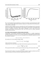
Figures 18b,c show SEM images of the PtIr probe-tip after 2.5 km and 5 km sliding distances
(corresponding to two weeks of continuous sliding) under the conditions mentioned above.
The wear volume is estimated to be 3.32×10
3
nm
3
after 2.5 km and 5.6×10
3
nm
3
after 5 km.
Figures 18d,e show a 3×1 matrix of inverted domain dots written by applying 100 µs wide
pulses of 5V before and after 5 km sliding, with the same domain sizes of 15.6 nm.
Although the tip has shown a small amount of wear, the write and read resolutions were
therefore not lost after 5 km of sliding at 5 mm/s.
Fig. 18. Wear tests on PtIr probe-tips sliding over a PZT surface with 0.17 nm RMS
roughness with force modulation and water lubrication (Tayebi et al., 2010b). (a-c) SEM
images of as received PtIr probe-tip prior to sliding (a), after 2.5 km (b) and 5 km (c) of
sliding at 5 mm/s with an applied normal force F
N
= 7.5 nN that is modulated at 200 kHz.
(d, e) PFM height (top), amplitude (middle) and phase (bottom) images of the PZT-film
surface with 3×1 matrix of 15.6 nm inverted domains formed by applying 100 µs pulses of 5
V using the probe-tip prior to (d) and after (e) the 5 km sliding experiment.
On the other hand, sliding experiments performed without force modulation while
keeping other conditions identical including the 25% RH level, showed a significant tip
blunting after only 500 m sliding with a tip wear volume of 8.2×10
5
nm
3
(Figures 19a,b).
Figures 19c,d show a 4×1 matrix of inverted domain dots written by applying 100 µs wide
pulses of 5V before and after the 500 m sliding. Here the dot size increased by 31.4 nm
from the as-received tip conditions. Therefore sliding under force modulation within the
elastic adhesive wear regime and in the presence of a thin water layer greatly reduces
wear. These results could lead to parallel-probe based data storage devices that exceed
the capabilities of current hard drive and solid state disks given the ultrahigh density
capabilities. It can also allow other scanning probe based systems such as AFM-based
lithograph.
Ferroelectrics - Applications
174
Fig. 19. Wear tests on PtIr probe-tips sliding over a PZT surface with 0.17 nm RMS roughness
without force modulation (Tayebi et al., 2010b). (a, b) SEM images of another PtIr probe-tip
prior (a) and after 500 m (b) of sliding at 5 mm/s with an applied normal force F
N
= 7.5 nN
without force modulation. (c) Height (top), amplitude (middle) and phase (bottom) images of
the film surface with 4×1 matrix of 15.6 nm inverted domains formed under the same
conditions using the PtIr probe-tip prior to the 500 m sliding experiment without modulation.
(d) Height (top), amplitude (middle) and phase (bottom) images of the film surface with 4×1
matrix of 47 nm inverted domains formed under the same conditions after the 500 m sliding
experiment. The size of the inverted domains increased by 31.2 nm after sliding.
6. Conclusions
This chapter reviewed recent progress to address several fundamental issues that have
remained a bottleneck for the development and commercialization of ultrahigh density
probe-based nonvolatile memory devices using ferroelectric media, including stability of
sub-10 nm inverted ferroelectric domains, reading schemes at high operating speeds
compatible with MEMS-based storage systems, and probe-tip wear.
Stable inverted domains less than 10 nm in diameter could be formed in ferroelectric films
when inversion occurred through the entire ferroelectric film thickness. Polarization
inversion was found to depend strongly on the ratio of the electrode size to the ferroelectric
film thickness. This is because full inversion minimized the effects of domain-wall and
depolarization energies by reducing the domain sidewalls and, thus enabling positive free
energy reduction rates. With this understanding, stable inverted domains as small as 4 nm
in diameter were experimentally demonstrated. Moreover, the reduction and suppression
of the built-in electric field, which would enhance the stability of sub-10 nm domains in up
and down-polarized ferroelectric PZT films, could be achieved by repetetive O
2
and H
2
plasma treatments to oxidize/reduce the PZT surface, thereby altering the electrochemistry
of the Pb over-layer. These treatments compensate for the negative charges induced by the
Pb vacancies that are at the origin of the built-in electric field.
Two probe-based reading techniques have shown potential compatibility with MEMS-based
probe storage systems at high speed rates: the charge-based scanning probe and the
Ultrahigh Density Probe-based Storage Using Ferroelectric Thin Films
175
scanning probe charge reading techniques. In the charge-based scanning probe read-back
microscopy, ferroelectric inverted domains are read back destructively by applying a
constant voltage that is greater than the coercive voltage of the ferroelectric film. In this
process, the flow of screening charges through the read-back amplifier provides sufficient
signal to enable the read of inverted domains as small as 10 nm with frequencies read-back
at rates as high as 1.5 MHz and speeds as high as 2 cm/s. For the case of the scanning probe
charge reading technique, the direct piezoelectric effect is used. The applied normal force
excreted by the probe-tip during scanning causes a charge buildup, which generates a
current when the probe tip travels across a domain wall of the inverted domain. Besides
reading at high speeds, this technique has the advantage of being nondestructive.
Lastly, we discussed a wear endurance mechanism which enabled a conductive PtIr coated
probe-tip sliding over a ferroelectric film at a 5 mm/s velocity to retain its write-read
resolution over a 5 km distance, corresponding to 5 years of device lifetime. This was
achieved by sliding the probe-tip at low applied forces on atomically smooth surfaces, with
force modulation, and in the presence of thin water films under optimized humidity. Under
the conditions of low applied forces on atomically smooth surfaces, the adhesive elastic
wear regime was dominant, and the wear rate was reduced by orders of magnitude. In this
regime, the wear volume is inversely dependent on the elastic modulus of the coating rather
than its hardness. Modulating the force in the presence of a thin water layer, which acts as a
viscoelastic film, further reduced the wear volume to insignificant amounts.
The novel solutions summarized in this chapter could lead to parallel-probe based data
storage devices that exceed the capabilities of current hard drive and solid state disks given
the ultrahigh density capabilities this technology possesses. While fundamental issues have
been addressed, the solutions were obtained at the single probe level. Therefore, these
solutions have to be tested and validated in actual devices, such as the Intel’s SSP memory
device (Heck et al., 2010) where 5000 MEMS cantilever-probes can simultaneously perform
write and read operations.
7. References
Ahn, C. H., Tybell, T., Antognazza, L., Char, K.; Hammond, R. H., Beasley, M. R.; Fischer,
Ø., and Triscone J M. (1997). Nonvolatile electronic writing of epitaxial
Pb(Zr
0.52
Ti
0.48
)O
3
/SrRuO
3
heterostructures, Science, Vol. 276, pp. 1100.
Ahn, C. H., Rabe, M. R., and Triscone, J M. (2004). Ferroelectricity at the nanoscale: Local
polarization in oxide thin films and heterostructures, Science, Vol. 303, pp. 488.
Bhushan, B., Kwak, K. J., and Palacio, M. (2008). Nanotribology and nanomechanics of AFM
probe-based data recording technology, Journal of Physics: Condensed Matter, Vol. 20,
pp. 365207.
Bhushan, B. (2002). Introduction to Tribology. New York, NY. John Wiley & Sons.
Cho, Y., Fujimoto, K., Hiranaga, Y., Wagatsuma, Y., Onoe, A., Terabe, K., and Kitamura, K.
(2003). Terabit/inch
2
ferroelectric data storage using scanning nonlinear dielectric
microscopy nanodomain engineering system, Nanotechnology, Vol. 14, pp. 637.
Cho, Y., Hashimoto, S., Odagawa, N., Tanaka, K., and Hiranaga, Y. (2005). Realization of 10
Tbit/in
2
memory density and subnanosecond domain switching time in
ferroelectric data storage, Applied Physics Letters Vol. 87, pp. 232907.
Ferroelectrics - Applications
176
Cho, Y., Hashimoto, S., Odagawa, N., Tanaka, K., and Hiranaga, Y. (2006). Nanodomain
manipulation for ultrahigh density ferroelectric data storage, Nanotechnology, Vol.
17, pp. S137.
Despont, L., Koitzsch, C., Clerc, F.; Garnier, M. G., Aebi, P., Lichtensteiger, C., Triscone, J
M., Garcia de Abajo, F. J., Bousquet, E. and Ghosez, Ph. (2006). Direct evidence for
ferroelectric polar distortion in ultrathin lead titanate perovskite films, Physical
Review B, Vol. 73, pp. 094110.
Fong, D. D., Stephenson, G. B., Streiffer, S. K., Eastman, J. A., Auciello, O., Fuoss, P. H. and
Thompson, C. (2004). Ferroelectricity in ultrathin perovskite films, Science, Vol. 304,
pp. 1650.
Forrester, M. G., Ahner, J. W., Bedillion, M. D., Bedoya, C., Bolten, D. G., Chang, K-C, de
Gersem, G., Hu, S., Johns, E. C., Nassirou, M., Palmer, J., Roelofs, A., Siegert, M.,
Tamaru, S., Vaithyanathan, V., Zavaliche, F., Zhao, T., and Zhao Y. (2009). Charge-
based scanning probe readback of nanometer-scale ferroelectric domain patterns at
megahertz rates, Nanotechnology Vol. 20,pp. 225501.
Garcia, V., Fusil, S., Bouzehouane, K., Enouz-Vedrenne, S., Mathur, N. D., Barthélémy, A.
and Bibes, M. (2009). Giant tunnel electroresistance for non-destructive readout of
ferroelectric states, Nature, Vol. 460, pp. 81.
Gotsmann, B. and Lantz, M. A. (2008). Atomistic wear in a single asperity sliding contact,
Physical Review Letters, Vol. 101, pp. 125501.
Hamann, H., O’Boyle, M., Martin, Y. C., Rooks, M., and Wickramasinghe, H. K. (2006).
Ultra-high-density phase-change storage and memory, Nature Materials, Vol. 5, pp.
383.
Hau, S.K. and Wong, K.H. (1995). Intrinsic resputtering in pulsed−laser deposition of
lead−zirconate−titanate thin films, Applied Physics Letters, Vol. 66, pp. 245.
Heck, J., Adams, D., Belov, N., Chou, T. A., Kim, B., Kornelsen, K., Ma, Q., Rao, V., Severi, S.,
Spicer, D., Tchelepi, G. and Witvrouw, A. (2010). Ultra-high density MEMS probe
memory device, Microelectronic Engineering, Vol. 87, pp. 1198.
Hiranaga, Y., Uda, T. Kurihashi, Y., Tanaka, K. and Cho, Y. (2007). Novel HDD-type SNDM
ferroelectric data storage system aimed at high-speed data transfer with single
probe operation. IEEE Transanctions on Ultrasonnics,.Ferroelectrics and Frequency
Control, Vol. 54, pp. 2523.
Junquera, J. and Ghosez, P. (2003). Critical thickness for ferroelectricity in perovskite
ultrathin films, Nature, Vol. 422, pp. 506.
Hong, S., Shin, H., Woo, J. and No, K. (2002). Effect of cantilever–sample interaction on
piezoelectric force microscopy, Applied Physics Letters, Vol. 80, pp. 1453
Kalinin, V., Karapetian, E. and Kachanov, M. (2004). Nanoelectromechanics of
piezoresponse force microscopy, Physical Review B, Vol. 70, pp. 184101.
Kim, B. M, Adams, D. E., Tran, Q., Ma, Q. and Rao, V. (2009). Scanning probe charge reading
of ferroelectric domains, Applied Physics Letters, Vol. 94, pp. 063105.
Kim, D. J., Jo, J. Y., Kim, Y. S., Chang, Y. J., Lee, J. S., Yoon, J. G., Song, T. K. and Noh, T. W.
(2005). Polarization relaxation induced by a depolarization field in ultrathin
ferroelectric BaTiO
3
capacitors, Physical Review Letters, Vol. 95, pp. 237602.
Knoll, A., Bächtold, P., Bonan, J., Cherubini, G., Despont, M., Drechsler, U., Dürig, U.,
Gotsmann, B., Häberle, W., Hagleitner, C., Jubin, D., Lantz, M.A., Pantazi, A.,
Pozidis, H., Rothuizen, H., Sebastian, A., Stutz, R., Vettiger, P., Wiesmann D. and
Ultrahigh Density Probe-based Storage Using Ferroelectric Thin Films
177
Eleftheriou, E.S. (2006). Integrating nanotechnology into a working storage device,”
Microelectronics Engineering, Vol. 83, pp. 1692.
Kim, Y. S ., Kim, D. H., Kim, J. D., Chang, Y. J., Noh, T. W., Kong, J. H., Char, K., Park, Y. D.,
Bu, S. D., Yoon, J G. and Chung, J S. (2005). Critical thickness of ultrathin
ferroelectric BaTiO
3
films, Applied Physics Letters, Vol. 86, pp. 102907.
Lantz, M. A., Gotsmann, B., Durig, U. T., Vettiger, P., Nakayama, Y., Shimizu, T. and
Tokumoto, H. (2003). Carbon nanotube tips for thermomechanical data storage,
Applied Physics Letter, Vol. 83, pp. 1266.
Lichtensteiger, C., Dawber, M., Stucki, N., Triscone, J M., Hoffman, J., Yau, J B., Ahn, C. H.,
Despont, L. and Aebi, P. (2007). Monodomain to polydomain transition in
ferroelectric PbTiO
3
thin films with La
0.67
Sr
0.33
MnO
3
electrodes, Applied Physics
Letters, Vol. 90, pp. 052907.
Li, X., Mamchik, A. and Chen, I W. (2001). Stability of electrodeless ferroelectric domains
near a ferroelectric dielectric interface, Applied Physics Letters, Vol. 79, pp. 809.
Miura, K. and Tanaka M, (1996). Origin of Fatigue in Ferroelectric Perovskite Oxides,
Japanese Journal of Applied Physics, Vol. 35, pp. 2719.
Nath, R., Chu, Y. –H, Polomoff, N. A., Ramesh, R., and Huey, B. D. (2008). High speed
piezoresponse force microscopy: <1 frame per second nanoscale imaging, Applied
Physics Letters, Vol. 93, pp. 072905.
Pantazi, A., Sebastian, A., Antonakopoulos, T. A., Bächtold, P., Bonaccio, A. R., Bonan, J.,
Cherubini, G., Despont, M., DiPietro, R. A., Drechsler, U., Dürig, U., Gotsmann, B.,
Häberle, W., Hagleitner, C., Hedrick, J. L., Jubin, D., Knoll, A., Lantz, M. A.,
Pentarakis, J., Pozidis, H., Pratt, R. C., Rothuizen, H., Stutz, R., Varsamou, M.,
Wiesmann, D., and Eleftheriou, E., (2008). Probe-based ultrahigh-density storage
technology, IBM Journal of Research and Development, Vol. 52, pp. 493.
Park, H., Jung, J., Min, D. -K., Kim, S., Hong, S. and Shin, H. (2004). Scanning resistive probe
microscopy: Imaging ferroelectric domains. Applied Physics Letters, Vol. 84, pp. 1734.
Petraru, A., Kohlstedt, H., Poppe, U., Waser, R., Solbach, A., Klemradt, U., Schubert, J.,
Zander, W. and Pertsev, N. A. (2008). Wedgelike ultrathin epitaxial BaTiO
3
films for
studies of scaling effects in ferroelectrics, Applied Physics Letters, Vol. 93, pp. 072902.
Tayebi, N., Nauru, Y., Franklin, N., Collier, C. P., Giapis, K. P., Nishi, N., and Zhang, Y.
(2010). Fully Inverted Single-Digit Nanometer Domains in Ferroelectric Films,
Applied Physics Letters
, Vol. 96, No. 2, pp. 023103.
Tayebi, N., Narui, Y., Chen, R. J., Collier, C. P., Giapis, K. P., and Zhang, Y. (2008a).
Nanopencil as a Wear-Tolerant Probe for Ultrahigh Density Data Storage, Applied
Physics Letters
, Vol. 93, No. 10, pp. 103112.
Tayebi, N., Zhang, Y., Chen, R. J., Tran, Q., Chen, R., Ma, Q., Nishi, Y., and Rao, V. (2010b)
An Ultraclean Tip-Wear Reduction Scheme for Ultrahigh Density Scanning Probe-
Based Data Storage, ACS NANO, Vol. 4, No. 10, pp. 5713-20.
Tayebi, N., Kim, S., Franklin, N., Chen, R J., Tran, Q., Ma, Q., Nishi, Y., and Rao, V.
(submitted). Tuning and Suppression of Built-in Electric Field for Long Term
Retention of Single-Digit Nanometer Domains in Ferroelectric Films.
Tybell, T., Ahn, C. H. and Triscone, J. -M. (1998). Control and imaging of ferroelectric
domains over large areas with nanometer resolution in atomically smooth epitaxial
Pb(Zr0.2Ti0.8)O3 thin films. Applied Physics Letters, Vol. 72, pp. 1454.
Ferroelectrics - Applications
178
Vettiger, P., Cross, G., Despont, M., Drechsler, U., Dürig, U., Gotsmann, B., Häberle, W.,
Lantz, M. A., Rothuizen, H. E., Stutz, R., and Binnig G. K. (2002). The ‘Millipede’ −
Nanotechnology entering data storage, IEEE Transactions on Nanotechnology, Vol. 1,
pp.
Wang, B. and Woo, C.H. (2003). Stability of 180° domain in ferroelectric thin films, Journal of
Applied Physics, Vol. 94, pp. 610.
Zhang, Z., Wu, P., Lu, L. and Shu, C. (2006). Study on vacancy formation in ferroelectric
PbTiO
3
from ab initio, Applied Physics Letters Vol. 88, pp. 142902.
Zhang, Z., Wu, P., Lu, L. and Shu, C. (2008). Ab initio study of formations of neutral
vacancies in ferroelectric PbTiO
3
at different oxygen atmospheres, Journal of Alloys
and Compounds Vol. 449, pp. 362.
Zhukovskii, Y. F., Kotominb, E. A., Piskunov, S. and Ellis, D.E., (2009). A comparative ab
initio study of bulk and surface oxygen vacancies in PbTiO
3
, PbZrO
3
and SrTiO
3
perovskites, Solid State Communications, Vol. 149, pp. 1359.
8
Fabrication and Study on One-Transistor-
Capacitor Structure of Nonvolatile Random
Access Memory TFT Devices Using
Ferroelectric Gated Oxide Film
Chien-Min Cheng, Kai-Huang Chen, Chun-Cheng Lin,
Ying-Chung Chen, Chih-Sheng Chen and Ping-Kuan Chang
Department of Electronics Engineering, Tung-Fang Design University,
Department of Electronic Engineering, Southern Taiwan University,
Department of Mathematics and Physics, Chinese Air Force Academy,
R.O.C.
1. Introduction
Recently, non-volatile and volatile memory devices such as static random access memory
(SRAM), dynamic random access memory (DRAM), Flash memory, EPROM and E
2
PROM
were very important for applications in conventional personal computer and micro-
processor, and performance efficiency of hardware improved by their low voltage, high
operation speed, and large storage capacity. The non-volatile memory devices were widely
investigated and discussed among these memory devices. Many kind of the non-volatile
memory device were ferroelectric random access memory (FeRAM), magnetron random
access memory (MRAM), and resist random access memory (RRAM) devices. Up to now,
the non-volatile ferroelectric random access memory (FeRAM) devices were attractive
because of their low coercive filed, large remnant polarization, and high operation speed
among various non-volatile access random memory devices [1].
The non-volatile FeRAM devices were limited by their relative larger one-transistor-one-
capacitor (1T-1C) size. Thus, one-transistor-capacitor (1TC) structure ferroelectric memory was
desirable because of the better sensitivity and small size than 1T-1C structure ferroelectric
memory [2-4]. The operation characteristics and reliability of ferroelectric capacitor structure of
1T-1C memory cell were spending lots cost during the fabrication process.
In addition, electronic devices and system-on-panel (SOP) technology were widely
discussed and researched. For SOP concept, the switch characteristics of various thin-film
transistor (TFT) structures were widely investigated for applications in amorphous silicon
(α-Si) and polycrystal silicon (poly-Si) active matrix liquid-crystal-display (AM-LCD)
displays [5-7]. Integrated electron devices such as memory devices, control devices, and
central processing units (CPU) on transparent conductive thin films will be important in the
future. The excellent electrical, physical, and reliability characteristics of metal-ferroelectric-
metal (MFM) capacitor structures for 1T1C memory cells were enhanced using transparent
conductive thin films on glass substrates.
Ferroelectrics - Applications
180
2. Electrical properties of non-volatile RAM using ferroelectric thin film
S. Y. Wu firstly reported that an MFS transistor fabricated by using bismuth titanate in 1974
[2-3]. The first ferroelectric memory device was fabricated by replacing the gate oxide of a
conventional metal-oxide-semiconductor (MOS) transistor with a ferroelectric material.
However, the interface and interaction problem between the silicon substrate and
ferroelectric films were very important factors during the high temperature processes in 1TC
structure. To overcome the interface and interaction problem, the silicon dioxide and silicon
nitride films were used as the buffer layer. The low remnant polarization and high operation
voltage of 1TC were also be induced by gate oxide structure with double-layer ferroelectric
silicon dioxide thin films. Sugibuchi et al. provided a 50 nm silicon dioxide thin film
between the Bi
4
Ti
3
O
12
layer and the silicon substrate [8].
Silicon Substrate
V
Al Al Al Al
Ferroelectric films
Al
Al
SiO
2
films
Silicon Substrate
Pt
V
Al Al Al Al
Ferroelectric films
Ti
SiO
2
films
Fig. 1. (a) Metal-ferroelectric-insulator-semiconductor (MFIS) structure, and (b) Metal
ferroelectric-metal (MFM) structure.
The ferroelectric ceramic target prepared, the raw materials were mixed and fabricated by
solid state reaction method. After mixing and ball-milling, the mixture was dried, grounded,
and calcined for some time. Then, the pressed ferroelectric ceramic target with a diameter of
two inches was sintered in ambient air. The base pressure of the deposited chamber was
brought down 1×10
-7
mTorr prior to deposition. The target was placed away from the
Pt/Ti/SiO
2
/Si and SiO
2
/Si substrate. For metal-ferroelectric-metal (MFM) capacitor
structure, the Pt and the Ti were deposited by dc sputtering using pure argon plasma as
bottom electrodes. The SiO
2
thin films were prepared by dry oxidation technology. The
metal-ferroelectric-insulator-semiconductor (MFIS) and metal-ferroelectric-metal (MFM)
structures were shown in Fig. 1.
For the physical properties of ferroelectric thin films obtained, the thickness and surface
morphology of ferroelectric thin films were observed by field effect scanning electron
microscopy (FeSEM). The crystal structure of ferroelectric thin films were characterized by
an X-ray diffraction (XRD) measurement using a Ni-filtered CuKα radiation. The
capacitance-voltage (C-V) properties were measured as a function of applied voltage by
using a Hewlett-Packard (HP 4284A) impedance gain phase analyzer. The current curves
versus the applied voltage (I-V characteristics) of the ferroelectric thin films were measured
by a Hewlett-Packard (HP 4156) semiconductor parameter analyzer.
Fabrication and Study on One-Transistor-Capacitor Structure of
Nonvolatile Random Access Memory TFT Devices Using Ferroelectric Gated Oxide Film
181
Additionally, the ferroelectric thin films were used in a one-transistor-capacitor (1TC)
structure of the amorphous-Si TFT device to replace the gate oxide of random access
memory devices. For that, a bottom-gate amorphous thin-film transistor, as shown in Fig.2,
would be fabricated and the characteristics of the fabricated devices were successfully
developed.
Silicon Substrate or ITO Substrate
Silicon Dioxide
Ti seed Layer
Pt bottom gate
Al DrainAl Source
n
+
Regionn
+
Region
Amorphous Silicon Layer
Ferroelectric Layer
Fig. 2. The 1TC FeRAM device fabricated with ferroelectric thin film.
For 1TC FeRAM device fabricated, a one-transistor-capacitor (1TC) structure of the
amorphous-Si (a-Si) TFT device was designed and fabricated. In Fig. 2, the a-Si TFT were
fabricated by depositing ferroelectric ferroelectric thin films gate oxide on bottom gate
Pt/Ti/SiO
2
/Si substrate. A silicon oxide film, acting as a buffer oxide, was deposited on
gate oxide substrate by plasma enhanced chemical vapor deposition (PECVD). A
amorphous silicon film, acting as an active channel, was also deposited by PECVD
method. Additionally, the source and drain regions were doped phosphorous by an ion
implantation method. A aluminum films was deposited as the source and drain
electrodes.
Finally, the a-Si TFT was heat treated for 1h in N
2
ambient for the purpose of alloying. The
a-Si TFT with the dimensions of 40 μm in width and 8 μm in length were designed and
fabricated and the I
D
-V
G
transfer characteristics of 1TC FeRAM devices were measured. The
operation characteristic of 1TC structure for TFT devices was similar to SONOS structure of
non-volatile flash memory device.
2.1 ABO
3
and BLSF
s
structure material
The (ABO
3
) pervoskite and bismuth layer structured ferroelectrics (BLSFs) were excellent
candidate materials for ferroelectric random access memories (FeRAMs) such as in smart
cards and portable electric devices utilizing their low electric consumption, nonvolatility,
high speed readout. The ABO
3
structure materials for ferroelectric oxide exhibit high
remnant polarization and low coercive filed. Such as Pb(Zr,Ti)O
3
(PZT), Sr
2
Bi
2
Ta
2
O
9
(SBT),
SrTiO
3
(ST), Ba(Zr,Ti)O
3
(BZ1T9), and (Ba,Sr)TiO
3
(BST) were widely studied and discussed
for large storage capacity FeRAM devices. The (Ba,Sr)TiO
3
and Ba(Ti,Zr)O
3
ferroelectric
materials were also expected to substitute the PZT or SBT memory materials and improve
the environmental pollution because of their low pollution problem [9-15]. In addition, the
Ferroelectrics - Applications
182
high dielectric constant and low leakage current density of zirconium and strontium-doped
BaTiO
3
thin films were applied for the further application in the high density dynamic
random access memory (DRAM) [16-20].
2.1.1 ABO3 pervoskite structure material system
For ABO
3
pervoskite structure such as, BaTiO
3
and BZ1T9, the excellent electrical and
ferroelectric properties were obtained and found. For SOP concept, the ferroelectric BZ1T9
thin film on ITO substrate were investigated and discussed. For crystallization and grain
grow of ferroelectric thin films, the crystal orientation and preferred phase of different
substrates were important factors for ferroelectric thin films of MIM structures. The XRD
patterns of BZ1T9 thin films with 40% oxygen concentration on Pt/Ti/SiO
2
/Si substrates
from our previous study were shown in Fig. 3 [21-22]. The (111) and (011) peaks of the
BZ1T9 thin films on Pt/Ti/SiO
2
/Si substrates were compared with those on ITO substrates.
The strongest and sharpest peak was observed along the Pt(111) crystal plane. This suggests
that the BZ1T9 films grew epitaxially with the Pt(111) bottom electrode. However, the (111)
peaks of BZ1T9 thin films were not observed for (400) and (440) ITO substrates. Therefore,
we determined that the crystallinity and deposition rate of BZ1T9 thin films on ITO
substrates differed from those in these study [21-24].
2θ de
g
ree
20 30 40 50 60
Intensity
ITO (400)
(011)
(001)
ITO (440)
(011)
(001)
(111)
(002)
(112)
Pt (111)
Electrical Field
-1500 -1000 -500 0 500 1000 1500
Polarization
-20
-10
0
10
20
5V
10V
15V
20V
Fig. 3. (a) XRD patterns of as-deposited thin films on the ITO/glass and Pt substrates, and
(b) P-E curves of thin films.
The polarization versus applied electrical field (P-E) curves of as-deposited BZ1T9 thin films
were shown in Fig. 3(a). As the applied voltage increases, the remanent polarization of thin
films increases from 0.5 to 2.5 μC/cm
2
. In addition, the 2P
r
and coercive field calculated and
were about 5 μC/cm
2
and 250 kV/cm, respectively. According to our previous study, the
BZ1T9 thin film deposited at high temperature exhibited high dielectric constant and high
leakage current density because of its polycrystalline structure [21].
2.1.2 Bismuth layer ferroelectric structure material system
Bismuth titanate system based materials were an important role for FeRAMs applications. The
bismuth titanate system were given in a general formula of bismuth layer structure
ferroelectric, (Bi
2
O
2
)
2+
(A
n-1
B
n
O
3n+1
)
2-
(A=Bi, B=Ti). The high leakage current, high dielectric loss
Fabrication and Study on One-Transistor-Capacitor Structure of
Nonvolatile Random Access Memory TFT Devices Using Ferroelectric Gated Oxide Film
183
and domain pinning of bismuth titanate system based materials were caused by defects,
bismuth vacancies and oxygen vacancies. These defects and oxygen vacancies were attributed
from the volatilization of Bi
2
O
3
of bismuth contents at elevated temperature [25-27].
2θ Degree
20 30 40 50 60
Intensity
STD
500
o
C
600
o
C
700
o
C
Pt (111)
(117)
(006)
(008)
(020)
(220)
(317)
Fig. 4. (a) XRD patterns of as-deposited Bi
4
Ti
3
O
12
thin films, and (b)The SEM morphology of
as-deposited Bi
4
Ti
3
O
12
films.
The XRD patterns of as-deposited Bi
4
Ti
3
O
12
thin films and ferroelectric thin films under
500~700
o
C rapid thermal annealing (RTA) process were compared in Fig. 4. From the results
obtained, the (002) and (117) peaks of as-deposited Bi
4
Ti
3
O
12
thin film under the optimal
sputtering parameters were found. The strong intensity of XRD peaks of Bi
4
Ti
3
O
12
thin film
under the 700
o
C RTA post-treatment were be found. They were (008), (006), (020) and (117)
peaks, respectively. Compared the XRD patterns shown in Fig. 4, the crystalline intensity of
(111) plane has no apparent increase as the as-deposited process is used and has apparent
increase as the RTA-treated process was used. And a smaller full width at half maximum
value (FWHM) is revealed in the RTA-treated Bi
4
Ti
3
O
12
thin films under the 700
o
C post-
treatment. This result suggests that crystal structure of Bi
4
Ti
3
O
12
thin films were improved in
RTA-treated process.
The surface morphology observations of as-deposited Bi
4
Ti
3
O
12
thin films under the 700
o
C
RTA processes were shown in Fig. 4. For the as-deposited Bi
4
Ti
3
O
12
thin films, the
morphology reveals a smooth surface and the grain growth were not observed. The grain
size and boundary of Bi
4
Ti
3
O
12
thin films increased while the annealing temperature
increased to 700
o
C. In RTA annealed Bi
4
Ti
3
O
12
thin films, the maximum grain size were
about 200 nm and the average grain size is 100 nm. As shown in Fig. 4, the thickness of
annealed Bi
4
Ti
3
O
12
thin films were calculated and found from the SEM cross-section images.
The thickness of the deposited Bi
4
Ti
3
O
12
thin films is about 800 nm and the deposited rate of
Bi
4
Ti
3
O
12
thin films is about 14 nm/mim.
2.1.3 The influence of doping effect on the electrical properties of ferroelectric films
In the past, we found that using V
2
O
5
as the addition or substitution would improve the
dielectric characteristics of SrBi
2
Ta
2
O
9
ceramics [28]. Vanadium doped Bi
4
Ti
3
O
12
thin films
were also found to have very large remanent polarization (2Pr) and the coercive field (Ec).
Ferroelectrics - Applications
184
But the leakage current density, the memory window and the changing ratio of memory
window of vanadium doped Bi
4
Ti
3
O
12
thin films measured using the MFIS structure were
not developed before [29-31].
Figure 5(a) shows ferroelectric hysteresis loops of Bi
4
Ti
3
O
12
and as-deposited BTV thin film
capacitors measured with a ferroelectric tester (Radiant Technologies RT66A). The as-
deposited BTV thin films clearly show ferroelectricity characteristics. The remanent
polarization and coercive field were 23 μC/cm
2
and 450 kV/cm. To compare the vanadium
doped and undoped Bi
4
Ti
3
O
12
thin films, the remanent polarization (2Pr) were increased
form 16μC/cm
2
for undoped Bi
4
Ti
3
O
12
thin films to 23 μC/cm
2
for vanadium doped.
However, the coercive field of as-deposited BTV thin films would be increased to 450
kV/cm. These results indicated that the substitution of vanadium was effective for the
appearance of ferroelectricity at 550 °C. The 2Pr value and the Ec value were larger than
those reported in Refs. [9-10], and the 2Pr value was smaller and the Ec value was larger
than those reported in [31]. Based on above results, it was found that the simultaneous
substitutions for B-site are effective to derive enough ferroelectricity by accelerating the
domain nucleation and pinning relaxation caused by B-site substitution [32-35].
Figure 5(b) shows the C-V curves of as-deposited vanadium doped BTV and un-doped BIT
thin films. The applied voltages, which are first changed from -20 to 20 V and then returned
to -20 V, are used to measure the capacitance voltage characteristics (C-V) of the MFIS
structures. For the vanadium doped thin films, the memory window of MFIS structure
increased from 5 to 15 V, and the threshold voltage decreased from 7 to 3 V. This result
demonstrated that the lower threshold voltage and decreased oxygen vacancy in undoped
BIT thin films were improved from the C-V curves measured.
Electrical Field (MV/cm)
-1000 -500 0 500 1000
Polarization (μC/cm
2
)
-30
-20
-10
0
10
20
30
undoped
vanadium doped
Applied Voltage(V)
-20 -15 -10 -5 0 5 10 15 20
Normalization Capacitance (nF)
0.4
0.6
0.8
1.0
vanadium doped
undoped
Fig. 5. (a) The P-E characteristics of vanadium doped and undoped thin films, and (b) The
normalization C-V curves of vanadium doped and undoped thin films.
According to pervious study, the Bi
4
Ti
3
O
12
materials exhibit high leakage current and
domain pinning properties because of the defects such as bismuth and oxygen vacancies.
The BTV thin film was prepared by substituting a bismuth ion with a lanthanum ion at A-
site substitution, and the fatigue endurance characteristics was improved [36]. In addition,
the B-site substitution by high-valent cation was mainly the compensation for the defects.
These defects caused by the fatigue phenomenon and strong domain pinning [37-40].
Fabrication and Study on One-Transistor-Capacitor Structure of
Nonvolatile Random Access Memory TFT Devices Using Ferroelectric Gated Oxide Film
185
Applied Voltage (V)
-30 -20 -10 0 10 20 30
Capacitance (nF)
2.10
2.15
2.20
2.25
2.30
2.35
2.40
2.45
BTV
BLTV
Electrical Field (kV/cm)
-600 -400 -200 0 200 400 600
Polarization (
μ
C/cm
2
)
-20
-10
0
10
20
BTV
BLTV
Fig. 6. (a) The C-V characteristics of as-deposited BTV and BLTV thin films, and (b) The P-E
characteristics of as-deposited BTV and BLTV thin films.
Figure 6(a) shows the change in the C-V curves of the BTV and BLTV thin films in MFM
structure measured at 100 kHz. The applied voltages, which were first changed from -20 to
20 V and then returned to -20 V, were used to measure the capacitance voltage
characteristics (C-V). The BLTV thin films exhibited high capacitance than those of BTV thin
films. We found that the capacitances of the lanthanum-doped BTV thin films were
increased.
Figure 6(b) shows the P-E curves of the different ferroelectric thin films under applied
voltage of 18V from the Sawyer−Tower circuits. The remanent polarization of non-doped,
vanadium-doped, and lanthanum-doped ferroelectric thin films linearly was increased from
5, 10 to 11 μC/cm
2
, respectively. The coercive filed of non-doped, vanadium-doped, and
lanthanum-doped ferroelectric thin films were about 300, 300, and 250 kV/cm, respectively.
The ferroelectric properties of lanthanum-doped and vanadium-doped BIT thin films were
improved and found.
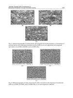
Fig. 7. The surface morphology of as-deposited BTV and BLTV thin films.
In Fig. 7, rod-like and circular-board grains were observed with scanning electron
microscopy (SEM) for as-deposited BTV films. The small grain was gold element in
preparation for the SEM sample. However, the BLTV thin films exhibited a great quantity
rod-like grain structure in Fig. 7. The rod-like grain size of BLTV thin films was larger than
those of BTV. We induced that the bismuth vacancies of BTV thin films compensate for
lanthanum addition and micro-structure were improved in BLTV thin films.
Ferroelectrics - Applications
186
2.2 Improved properties for ferroelectric films using post-treatment technology
The electrical and physical characteristics were affected by defect and oxygen vacancy of
grain boundary in various oxide materials for applications in electrical integrated circuits.
The defects and oxygen vacancies in conventional oxide films were usually filled and
compensated by oxygen gas using different deposition methods in the semiconductor
manufacturing process. The crystal structure of the various oxide films was improved by the
high deposition temperature. However, the oxygen elements in grain boundary of the thin
films were broken and lost above the deposition temperatures of 550
o
C [41–47]. To improve
the properties of various oxide materials under the post-treatment process, the conventional
temperature annealing (CTA) and rapid thermal annealing (RTA) processing were
sometimes essential and indispensable technology for crystallization and quality of thin
films [48-52].
2.2.1 CFA and RTA post-treatment technology
Ferroelectric thin films prepared by rapid temperature annealing (RTA) and conventional
temperature annealing (CFA) processing were reported extensively. Many studies had been
reported that rapid temperature annealing method was successfully to increase the electrical
and physical properties [53-56]. In addition, grain size, electrical properties and surface
roughness are greatly affected by annealing temperature under conventional furnace
annealing.
To study the characteristics of thin films of perovskite oxide BZ1T9, deposited on ITO glass
substrate using the different RTA annealing temperatures were found. In which, the
characteristics of the Al/BZ1T9/ITO glass (MFM) structures, were reported and the
relationship between the electrical properties and different annealing temperature of MFM
structure was investigated. In addition, preferred orientation, crystal phase and dielectric
properties of BZ1T9 thin films by different annealing temperatures were discussion and
evaluated.
Fig. 8. (a) The C-V characteristics of as-deposited and RTA-treated thin films, and (b) The P-
E characteristics of RTA-treated thin films.
Figure 8(a) shows the C-V curves of as-deposited and annealed BZ1T9 films when applied
voltage of ±20V. From the experiments obtained, the capacitance of RTA annealed BZ1T9
films increased while the temperature increased to 650
o
C. Besides, the maximum dielectric
Fabrication and Study on One-Transistor-Capacitor Structure of
Nonvolatile Random Access Memory TFT Devices Using Ferroelectric Gated Oxide Film
187
constant of RTA annealed BZ1T9 films were found. In addition, the larger grain size of
annealed BZ1T9 films were attributed to this reason.
The leakage current density versus applied electrical field (J-E) curves of as-deposited
BZ1T9 films under 650
o
C RTA process were also found. The leakage current densities of as-
deposited BZ1T9 films using RTA process were about 2×10
-6
A/cm
2
under the electrical field
of 0.5 MV/cm. It showed that the leakage current density of annealed-BZ1T9 films was
larger than those of as-deposited BZ1T9.
The P-E curves of as-deposited BZ1T9 thin films at a frequency of 100 kHz was shown in
Fig. 8(b). As the applied voltage increases, the remanent polarization of thin films increases.
In addition, the 2P
r
and coercive field are also calculated and were about 6 μC/cm
2
and 250
kV/cm, respectively. According to our previous study, the BZ1T9 thin film deposited at a
higher temperature exhibits a higher dielectric constant and a higher leakage current density
because of its polycrystalline structure [57].
2.2.2 Oxygen plasma post-treatment technology
The high-temperature process for integrated fabrication on electronic devices was a
serious problem. The gas-like and excellent properties of the oxygen plasma process were
attracted considerable research in efficiently transporting oxygen atom and nodamaging
diffusion into the microstructures of oxide materials at a low-temperature treatment.
Decreased and passivated the traps and defects of oxide materials were the most
advantages.
Figure 9(a) shows the leakage current density versus electrical filed (J-E) curves of as-
deposited BSTZ thin films treated as a function of oxygen plasma treatment times. The
leakage current density of BSTZ thin films was decreased as oxygen plasma treatment times
increased. The leakage current density of treated thin films was lower than those of as-
deposited thin films. We also found that the leakage current density of the BSTZ thin films
for 3 minutes plasma treatment time were similar to those for 6-9 minutes plasma
treatment time. To discuss the defects and oxygen vacancies effect, the leakage current
versus electrical field curves were fitted to the Schottky emission and Poole-Frankel
transport models [58−60]. The fitting curve was straight line, and the J−E curves of as-
deposited thin films after oxygen plasma treatment obey the Schottky emission model in fig.
2. From the experimental results, the low leakage current density of plasma treated thin
films was attributed to less oxygen defects and vacancies.
Figure 8(b) shows the capacitances-voltage (C-V) curves of non-treatment and oxygen
plasma treatment BSTZ thin films. The capacitance of thin films was increased while the
oxygen treatment time increased. The capacitance of thin films was increased. As the results,
the improvement of capacitance of BSTZ thin films were attributed to the oxygen ion
vacancy compensated.
In addition, we found that the wide-scan XPS spectrum of the as-deposited thin film for
oxygen plasma treatment in the binding energy range from 100 to 1keV. From the XPS
spectrum, it revealed that the thin films contained Ba 3d, Sr 3d, Ti 2p, Zr 3d, and O 1s
elements. After oxygen plasma treated, the LBE and HBE were increased to 533.6 and 535.8
eV. These results induced that the oxygen plasma operatively react with the dangling bonds
of thin films and form the stronger O 1s bonding. The O 1s binding energy of the BSTZ thin
film after oxygen plasma treatment was increased.
Ferroelectrics - Applications
188
Electrical Field (MV/cm)
0.00.10.20.30.40.5
Leakage Current Density (A/cm
2
)
10
-10
10
-9
10
-8
10
-7
10
-6
10
-5
10
-4
10
-3
0%
25%
40%
60%
Applied Voltage (V)
-10 -5 0 5 10
Capacitance (pF)
100
150
200
250
300
350
STD
1 min
3 min
6 min
9 min
Fig. 9. (a) The J-E characteristics of as-deposited and plasma-treated BSTZ thin films, and (b)
The C-V characteristics of as-deposited and plasma-treated BSTZ thin films.
For other ferroelectric thin film, the leakage current density versus applied voltage (J-E)
curves of the BZ1T9 thin films was shown in Fig. 5. At an electric field of 0.25 MV/cm, the
oxygen-plasma-treated films exhibit a leakage current density two orders of magnitude
lower than those of the non-oxygen-plasma-treated ones. As mentioned above, the oxygen
plasma treatment decreases the oxygen vacancies and the leakage current density.The
current-field curves were fit to Schottky emission and Poole-Frankel transport models to
determine whether the observed decrease in leakage current of the oxygen plasma treated
films [58-60]. Smyth et al. reported that oxygen escapes during thermal process, and the
oxygen vacancies are subsequently generated according to O
o
<-> V
o
++
+ 2e
-
+ 1/2 O
2
, that
the O
o
, V
o
++
, and e
-
denote the oxygen ion at its normal site, oxygen vacancy, and electron,
respectively. For that, a lot of oxygen vacancies will exist after 9 min the oxygen plasma
treatment.
Electrical Field (MV/cm)
-0.25 0.00 0.25
Polarization (μC/cm
2
)
-20
-10
0
10
20
No plasma treated
Oxygen plasma treated
Electrical Field
(
MV/cm
)
0.00 0.05 0.10 0.15 0.20 0.25 0.30
Leakage Current Density (A/cm
2
)
10
-8
10
-7
10
-6
10
-5
No plasma treated
6 min plasma treated
9 min plasma treated
Fig. 10. (a) The P-E characteristics of as-deposited and plasma-treated BZ1T9 thin films, and
(b) The J-E characteristics of as-deposited and plasma-treated BZ1T9 thin films.
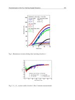
Figure 10(a) shows the P-E curves of the BZ1T9 films observed at a frequency of 100 kHz
under an applied electrical field of 0–0.28 MV/cm from the Sawyer-Tower circuits. After
oxygen plasma treatment, the coercive field does not appear to change; however, the
remnant polarization appears to increase from 6 to 9 μC/cm2. As shown in Fig. 10(b), we
Fabrication and Study on One-Transistor-Capacitor Structure of
Nonvolatile Random Access Memory TFT Devices Using Ferroelectric Gated Oxide Film
189
observed that the saturation polarization decreases slightly when an electrical field of 280
kV/cm was applied. This effect can be caused by the high leakage current density under
stronger electrical fields.
2.2.3 Supercritical carbon dioxide fluid technology
To discuses and investigate the electrical, physical, and ferroelectric properties of as-deposited
thin films, the supercritical carbon dioxide fluid (SCF) process were used by a low temperature
treatment. The ferroelectric thin films were post-treated by SCF process which mixed with
propyl alcohol and pure H
2
O. After SCF process treatment, the remnant and saturation
polarization increased in hysteresis curves, and the passivation of oxygen vacancy and defect
in leakage current density curves were found. Besides, the qualities of as-deposited
ferroelectric thin films using SCF process treatment were carried out XPS, C-V, and J-E results.
Applied Voltage (V)
-8 -6 -4 -2 0 2 4 6 8
Capacitance (nF)
2.6
2.8
3.0
3.2
STD
SCCO
2
treatment
Electrical Field (kV/cm)
-1000 -500 0 500 1000
Polarization (
μ
C/cm
2
)
-30
-20
-10
0
10
20
30
STD
SCCO
2
treatment
Fig. 11. (a) The C-E characteristics of as-deposited and SCCO
2
-treated BZ1T9 thin films, and
(b) The J-E characteristics of as-deposited and SCCO
2
-treated BZ1T9 thin films.
Figure 11(a) compares the change in the capacitance versus the applied voltage (C-V) for the
non-treatment and SCCO
2
fluid treatment BZ1T9 thin films. The applied bias voltage ranges
from -20 to 20 V. The capacitances of the BZ1T9 thin films appear to increase due to the
SCCO
2
fluid treatment. The capacitances increase from 2.65 to 2.95 nF were found after the
post-treatment. As suggested by the XPS analysis result, the improvement in the capacitance
of the BZ1T9 thin films were attributed to the compensation of the oxygen vacancy of the
ABO
3
phase in the BZ1T9 thin films.
Figure 11(b) shows the P-E curves of the thin films observed at a frequency of 500 kHz
under a 20V applied voltage from the Sawyer-Tower circuits. After SCCO
2
fluid treatment,
the 2Pr value and coercive filed of BZ1T9 thin films for MIM structure were about 20
μC/cm
2
and 250kV/cm, respectively. We found that remnant polarization were improved
and increased from 3 to 10 μC/cm
2
.
Figure 12(a) shows the wide-scan XPS spectrum of the BZ1T9 thin film in the binding
energy range from 200 to 900 eV. From the spectrum it is clear that the BZ1T9 film contains
Ba, Zr, Ti, and O elements near its surface, and no other impurity element was detected in
the spectrum up to 900 eV. Quantitative XPS analysis result not only provides the chemical
composition near the sample surface, but also gives the formation on the chemical bonding.
From the spectrum of the chemical bonding observed, the compounds of the surface for
BZ1T9 thin films would be determined. In addition, the narrow-scan XPS spectra of O 1s
peaks for the BZ1T9 thin film were shown in Fig. 12(b).
Ferroelectrics - Applications
190
Binding Energy
300 400 500 600 700 800
Intensity
STD
SCCO
2
treatment
Ba 3d
O 1s
Ti 2p
Zr 3d
Binding Energy
528530532534536
Intensity
STD
SCCO
2
treatment
Fig. 12. (a)Wide-scan XPS spectrum and (b) O 1s energy levels of ferroelectric thin film after
SCCO
2
fluid treatment.
To infer the variation in chemical bonding of BZ1T9 thin films during processing with
SCCO
2
fluid treatment, a doublet structure was observed in the XPS spectrum of O 1s peak
were found. Its component peak in the spectrum was fitted to a Guassian type distribution
with lower binding energy (LBE) and higher binding energy (HBE) peaks at 529.62 eV and
531.68 eV, respectively. The LBE peak was due to the oxide and the HBE peak was due to
the hydroxide/absorbed oxygen. These results induced that indicating that the H
2
O
molecules indeed can operatively react with the thin films dangling bonds (or traps) and
form the stronger O 1s bonding.
2.3 Fabrication ferroelectric random access memory device on bottom-gated
amorphous silicon thin-film transistors
Recently, the ferroelectric BZ1T9 composition was used in a one-transistor-capacitor (1TC)
structure of the amorphous-Si TFT device to replace the gate oxide of random access
memory devices. For that, a bottom-gate amorphous thin-film transistor, as shown in
Fig. 13, was fabricated and the characteristics of the fabricated devices were developed.
The counter clockwise current hysteresis and memory window of n-channel thin-film
transistor property were observed, and that were be used to indicate the switching of
ferroelectric polarization of BZ1T9 thin films. Additionally, the ferroelectric random access
memory device using bottom-gate amorphous silicon thin-film transistor with channel
width=40 μm and channel length=8 μm has been successfully fabricated and the I
D
-V
G
transfer characteristics were also investigated.
Fig. 13. The top view of the 1TC FeRAM device fabricated with BZ1T9 as the bottom-gate
oxide.
Fabrication and Study on One-Transistor-Capacitor Structure of
Nonvolatile Random Access Memory TFT Devices Using Ferroelectric Gated Oxide Film
191
After the optimum characteristics of BZ1T9 thin films were deposited, then the BZ1T9 thin
films obtained at the optimum parameters were used to fabricate the one-transistor-capacitor
(1TC) structure of the amorphous-Si TFT device, and the top view of the fabricated 1TC
FeRAM device with BZ1T9 gate oxide was shown. The measured transfer characteristics of
drain current and gate voltage (I
D
-V
G
) of the fabricated ferroelectric gate oxide 1TC FeRAM
device were shown in Fig. 14. The a-Si TFT device using BZ1T9 gate oxide measured from the -
5 to 20 V and then from 20 return to -5 V at drain voltage from 0.1 to 5V.
Gate Voltage (V)
-10-5 0 5 101520
Drain Current (A)
10
-7
10
-6
10
-5
10
-4
VD=0.1 V
VD=1.5 V
VD=4.5 V
Drain Volta
g
e (V)
0246810
Drain Current (A)
10
-7
10
-6
10
-5
10
-4
10
-3
Fig. 14. I
D
-V
G
transfer characteristics of the fabricated 1TC FeRAM devices.
The counterclockwise current hysteresis and memory window of n-channel thin-film
transistor property as indicated by arrows were observed, and the I
D
-V
G
transfer
characteristics were used to indicate the switching of ferroelectric polarization of BZ1T9 thin
films. From the measured results, the drain current is less than 1×10
-7
A around V
G
=-1V and
larger drain current of 4×10
-5
A as V
G
=10V were found. It was interesting to note that the
memory windows are 12 and 20V, respectively, when the drain voltages are increased from
0.1 to 5V. As Fig. 14 shows, the threshold voltage and sub-threshold characteristics were
obtained, and threshold voltage was about -4V. Besides, the on/off drain current ratio was
about the magnification of two orders. The on/off current ratio obtained from the fabricated
1TC FeRAM device in this study was much smaller than that of the most reported bottom-
gated TFTs devices by using different ferroelectric materials as gate oxide.
Figure. 14 shows the measured drain current versus drain voltage (I
D
–V
D
) characteristics of
1TC FeRAM devices with a channel length of 30 μm. The 1TC FeRAM device has properties
typical of n-channel transistors and exhibits clear current saturation. In addition, the (I
D
–V
D
)
current window was found at V
G
= 10 V. This was because the ferroelectric gate insulator can
induce a considerably large charge. As shown in Fig. 14, we obtained an on-current of 5×10
–5
A
for the 1TC FeRAM devices with a channel length of 30 μm.
3. Conclusion
The post-treatment technology, such as CTA, RTA, SCCO
2
and oxygen plasma treatment
was an effective method to remove the vacancies and defects for as-deposited ferroelectric
thin films. The post-treatment technology was developed to take the oxygen molecules to
terminate the traps for as-deposited thin films. The improvement effect in the leakage
current mechanism of the as-deposited thin film using post-treatment technology was
discussed. The capacitance increased for reduction of interface states and passivation of
traps in the as-deposited thin films treated by post-treatment technology was observed.
Ferroelectrics - Applications
192
Besides, the one-transistor-capacitor (1TC) structure of ferroelectric random access memory
(FeRAM) with the gate oxide of BZ1T9 thin films on the amorphous-Si TFT structure were
investigated and fabricated. The on/off drain current ratio was two orders (10
2
), and the
value was much smaller than those of the most reported bottom-gated TFTs devices by
using different ferroelectric materials as gate oxide. From these results in our study, the
BZ1T9 thin film for bottom-gate amorphous-Si thin-film transistor was an excellent
candidate to fabricate higher storage capacitance ferroelectric random access memory
devices.
4. Acknowledgment
The authors will acknowledge to Prof. Ting-Chang Chang and Prof. Cheng-Fu Yang.
Additionally, this work will acknowledge the financial support of the National Science
Council of the Republic of China (NSC 99-2221-E-272-003) and (NSC 97-2221-E-272-001).
5. References
[1] J. M. Kim, D. S. Yoon, and K. No: J. Mater. Sci. 29 (1994) 6599.
[2] S. Y. Wu: IEEE Trans. Electron Devices 21 (1974) 499.
[3] S. Y. Wu: Ferroelectrics 11 (1976) 379.
[4] H. Buhay, S. Sinharoy, W. H. Kasner, M. H. Francombe, D. R. Lampe, and E. Stepke:
Appl. Phys. Lett. 58 (1991) 1470.
[5] P. T. Liu, Y. T. Chou, L. F. Teng, F. H. Li, H. P. Shieh: Appl. Phys. Lett. 98 (2011) 052102.
[6] J. S. Park, T. S. Kim, K. S. Son, W. J. Maeng, H. S. Kim, M. Ryu, and S.g Y. Lee: Appl.
Phys. Lett. 98 (2011) 012107.
[7] M. Kimura, T. Kamiya, T. Nakanishi, K. Nomura, and H. Hosono: Appl. Phys. Lett. 96
(2010) 262105.
[8] K. Sugibuchi, Y. Kurogi and N. Endo: J. Appl. Phys., 46 (1975) 2877.
[9] I. G. Ismailzade, V. I. Nesterenko, Sov. Phys. Crystallogr. 12 (1968) 625.
[10] M. Kimura, T. Sawada, A. Ando, Y. Sakabe, Jpn, J. Appl. Phys. 38 (1998) 5557.
[11] J. F. Scott and C. A. Paz de Araujo, Science 246, 1400 (1989).
[12] D. J. Taylor, R. E. Jones, P. Zurcher, P. Chu, Y. T. Lii, B. Jiang, and S. J. Gillespie, Appl.
Phys. Lett. 68, 2300 (1996).
[13] J. F. Scott and C. A. Paz de Araujo, Science 246, 1400 (1989).
[14] C. A. Araujo, J. D. Cuchiaro, L. D. McMillian, M. C. Scott, and J. F. Scott, Nature
(London) 374, 627 (1995).
[15] B. H. Park, B. S. Kang, S. D. Bu, T. W. Noh, J. Lee, and W. Jo, Nature (London) 401, 682
(1999).
[16] C. C. Leu, L. R. Yao, C. P. Hsu, and C. T. Hu, J. Electrochem. Soc., 157, 3, (2010) G85.
[17] K. H. Chen, Y. C. Chen, C. F. Yang, and T. C. Chang, J. Phys. Chem. Solids, vol. 69,
(2008) 461.
[18] C. F. Yang, K. H. Chen, Y. C. Chen, and T. C. Chang, IEEE Trans. Ultrason. Ferroelectr.
Freq. Control, 54 (2007) 1726.
[19] C. F. Yang, K. H. Chen, Y. C. Chen, and T. C. Chang, Appl. Phys. A, 90 (2008) 329.
[20] K. H. Chen, Y. C. Chen, Z. S. Chen, C. F. Yang, and T. C. Chang, Appl. Phys. A, 89
(2007) 533.
[21] G. Velu, C. Legrand, O. Tharaud, A. Chapoton, D. Remiens, and G. Horowitz, Appl.
Phys. Lett. 79 (2001) 659.
Fabrication and Study on One-Transistor-Capacitor Structure of
Nonvolatile Random Access Memory TFT Devices Using Ferroelectric Gated Oxide Film
193
[22] K. H. Chen, Y. C. Chen, C. F. Yang, and T. C. Chang: J. Phys. Chem. Solids 69 (2007) 461.
[23] K. H. Chen, C. F. Yang, C. H. Chang, Y. J. Lin : J. Jap. Appl. Phys., 48 (2009) 091401.
[24] J. Miao, J. Yuan, H. Wu, S. B. Yang, B. Xu, L. X. Cao, and B. R. Zhao, Appl. Phys. Lett. 90
(2001) 022903.
[25]C. F. Yang, K. H. Chen, Y. C. Chen, and T. C. Chang: Appl. Phys. A 90 (2008) 329.
[26] T. Kijima and H. Matsunaga, Jpn. J. Appl. Phys. 38, (1999) 2281.
[27] T. Watanabe, H. Funakubo, M. Osada, Y. Noguchi and M. Miyayama, Appl. Phys. Lett.
80, No.1 (2002).
[28] S. S. Kim, T. K. Song, J. K. Kim and J. Kim, J. Appl. Phys. 92, No.4 (2002)
[29] Y. Noguchi and M. Miyayama, Appl. Phys. Lett. 78, No.13 (2001).
[30] E. K. Choi, S. S. Kim, J. K. Kim, J. C. Bae, W. J. Kim, Y. I. Lee, T. K. Song, Jpn. J. Appl.
Phys,Part 1. 43 (1) (2004 ) 237.
[31]B. H. Park, B. S. Kang, S. D. Bu, T. W. Noh, L. Lee, and W. Joe, Nature (London) 401, 682
(1999).
[32] Y. Noguchi, I. Miwa, Y. Goshima, and M. Miyayama, Jpn. J. Appl. Phys., Part 2 39,
L1259 (2000).
[33] Y. Noguchi and M. Miyayama, Appl. Phys. Lett. 78, 1903 (2001).
[34] T. Friessnegg, S. Aggarwal, R. Ramesh, B. Nielsen, E. H. Poindexter, and D. J. Keeble,
Appl. Phys. Lett. 77, 127 (2000).
[35] W. Takayuki, F. Hiroshi, O. Minoru, N. Yuji, M. Masaru, Appl. Phys. Lett. 80, (2002) 100.
[36] B. H. Park, B. S. Kang, S. D. Bu, T. W. Noh, L. Lee, and W. Joe, Nature (London) 401,
(1999) 682.
[37] X. J. Meng, J. H. Ma, J. L. Sun, T. Yu, J. Lin, G. S. Wang, J. H. Chu, Appl. Phys. Lett. 78,
(2004) 1089.
[38] B. H. Park, B. S. Kang, S. D. Bu, T. W. Noh, L. Lee, and W. Joe, Nature (London) 401,
(1999) 682.
[39] Y. Noguchi, I. Miwa, Y. Gosima, and M. Miyayama, Jpn. J. Appl. Phys., Part 2 39, (2000)
L1259.
[40] Y. Noguchi and M. Miyayama, Appl. Phys. Lett. 78 (2001) 1903.
[41] T. Friessnegg, S. Aggarwal, R. Ramesh, B. Nielsen, E. H. Poindexter, Jpn. J. Appl. Phys.,
Part 1 40 (2001) 5572.
[42] P. Orgiani, R. Ciancio, A. Galdi, S. Amoruso, and L. Maritato, Appl. Phys. Lett. 96 (2010)
032501.
[43] W. Lim, E. A. Douglas, D. P. Norton, S. J. Pearton, F. Ren, Y. W. Heo, S. Y. Son, and J. H.
Yuh, Appl. Phys. Lett. 96, (2010) 053510.
[44] D. Y. Wang, S. Li, H. L. W. Chan, and C. L. Choy, Appl. Phys. Lett. 96, (2010) 061905.
[45] C. C. Lin and C. C. Lee, J. Electrochem. Soc., 157, 2, (2010) A230.
[46] K. Tajima, Y. Yamada, S. Bao, M. Okada, and K. Yoshimura, J. Electrochem. Soc., 157, 3,
(2010) J92.
[47] N. C. Su, S. J. Wang, and Albert Chin, Electrochem. Solid-State Lett., 13, 1, (2010) H8.
[48] O. Tuna, Y. Selamet, G. Aygun and L. Ozyuzer, J. Phys. D, 43 (2010) 055402.
[49] K. F. Chiu, C. C. Chen, M. H. Chiang, and W. H. Ho, J. Electrochem. Soc., 157, 2, (2010)
A130.
[50] C. C. Chen, K. F. Chiu, K. M. Lin, H. C. Lin, C. R. Yang, F. M. Wang, and M. H. Chiang,
J. Electrochem. Soc., 157, 3, (2010) A289.
[51] M. Furuta, T. Nakanishi, M. Kimura, T. Hiramatsu, T. Matsuda, H. Furuta, T.
Kawaharamura, C. Li, and T. Hirao, Electrochem. Solid-State Lett., 13, 4, (2010)
H101.
Ferroelectrics - Applications
194
[52] S. J. Won, S. S. Sang, W. Lee, G. J. Choi, C. S. Hwang, and H. J. Kim, Electrochem. Solid-
State Lett., 13, 2, (2010) G13.
[53] C. L. Sun, P. C. Juan, Y. W. Hsu and Y. W. Liu, Thin Solid Films, 518, 24, (2010) 7433.
[54]C. F. Yang, K. H. Chen, Y. C. Chen, and T. C. Chang, Appl. Phys. A, 90, 2, (2008) 329.
[55] A. D. Li, D. Wu, H. Q. Ling, M. Wang, Z. Liu and N. Ming, J. Cryst. Growth, 235 (2002)
394.
[56] V. R. Palkar, S. Chattopadhyay, S. C. Purandare, S. G. Lokhre, R. Pinto and M. S.
Multani, Mater. Lett.33 (1997) 1.
[57] J. Li, L. Zhang, X. Yao and J. Wang, Ceram. Int., 30 (2004) 1509.
[58] M. L. Calzada, A. Gonzalez, R. Jimenez, C. Alemany and J. Mendiola, J. Euro. Ceram.
Soc. 21 (2001) 1517.
[59] Y. Wang, L. Li, J. Qi and Z. Gui, Ceram. Int. 28, 6 (2002) 657.
[60] K. H. Chen, Y. C. Chen, C. F. Yang, and T. C. Chang: J. Phys. Chem. Solids 69 (2007) 461.
[61] S. Fleischer, P. T. Lai, and Y. C. Cheng, J. Appl. Phys. 73 (1994) 8353.
[62] T. Mihara and H. Watanabe, Part I, Jpn. J. Appl. Phys. 34 (1995) 5664.
[63] Y. B. Lin and J. Y. Lee, J. Appl. Phys. 87 (2000) 1841.
[64] T. A. Rost, H. Lin and T. A. Rabson, Appl. Phys. Lett., 59 (1991) 3654.
[65] M. Yoshimoto, M. Anami, H. Shinohara, T. Yoshihara, H. Takagi, S. Nagao, S. Kayano
and T.Nakano: IEEE Trans., Solid State Circuits, 18 (5) (1983) 479.
[66] T. Matsuda, K. Miyoshi, R. Yamaguchi, S. Moriya and T. Hosoya, K. Harada: IEEE
Trans., Solid State Circuits, 20 (1) (1985) 88.
[67] J. Welser, S. Tiwari, S. Rishton, K. Lee and Y. Lee: IEEE Trans., Electron Device Lett., 18
(6)(1997) 278.
[68] N. Young, G. Harkin, R. Bunn, D. McCulloch and I. French: IEEE Trans., Electron
Device,43 (11) (1991) 1930.
[69] S. Y. Wu: IEEE Trans., Electron Devices, (1974) 499.
[70] S. Y. Wu: Ferroelectr., 11 (1976) 379.
[71] H. Buhay, S. Sinharoy, W. H. Kasner, M. H. Francombe, D. R. Lampe and E. Stepke,
Appl. Phys. Lett., 58 (1991) 1470.
[72] K. Sugibuchi, Y. Kurogi and N. Endo: J. Appl. Phys., 46 (1975) 2877.
[73] T. A. Rost, H. Lin, T. A. Rabson, R. C. Baumann and D. C. Callahan, IEEE Trans.
Ultrason. Ferroelectr. Freq. Control, 38 (1991).
[74] S. R. Shannigrahi and H. M. Jang, Appl. Phys. Lett., 79 (2001)1051.
[75] S. K. Hong, C. W. Suh, C. G. Lee, S. W. Lee, E. Y. Hang and N. S. Kang: Appl. Phys.
Lett., 77 (2000) 76.
[76] S. B. Xiong and S. Sakai: Appl. Phys. Lett., 75 (1999) 1613.
[77] J. S. Kim and S. G. Yoon: J. Vac. Soc. Technol., B 18 (1) (2000) 216.
[78] T. B. Wu, C. M. Wu and M. L. Chen: Appl. Phys. Lett., 69 (1996) 2659.
[79] M. She, H. Takeuchi and T. J. King: IEEE Trans., Electron Device Lett., 25 (5) (2003) 309.
[80] Y. K. Lee, J. S. Sim, S. K. Sung, C. J. Lee, T. H. Kim and J. D. Lee: IEEE Trans., Electron
Device Lett., 23 (11) (2002) 664.
[81] M. W. J. Prins, K. O. Grosse-Holz, G. Muller, J. F. M. Cillessen, J. B. Giesbers, R. P.
Weening and R. M. Wolf: Appl. Phys. Lett., 68 (1996) 3650.
[82] T. Miyasako, M. Senoo and E. Tokumitsu: Appl. Phys. Lett., 86 (2005).
1. Introduction
Flexible electronic devices and systems fabricated on bendable, rollable, and stretchable
plastic substrate define important application fields of novel paradigm for next-generation
”consumer electronics”. In these fields, such features as good design, ultra-low cost, and
unique functionality would be primarily demanded, which is totally different from the case
of conventional Si-based electronics. Recently, many types of interesting approaches have
been actively researched and developed. Flexible displays (Gelinck & Leeuw, 2004; Park
J. S. et al., 2009), radio-frequency flexible identification tags (Forrest, 2004; Jung M. et al.,
2010), flexible and stretchable sensor arrays (Lin K. & Jain, 2009; Someya et al., 2005), flexible
electronic circuit systems (Graz & Lacour, 2009; Zschieschang et al, 2010), stretchable lightings
(Sekitani et al., 2009a), printable devices (Ishida et al., 2010), and sheet-type communication
and power-transmission system (Sekitani et al., 2009b) are the feasible examples. In order
to develop the practical systems using these devices, an embeddable nonvolatile memory is
strongly required as one of the core devices. The employment of suitable memory device into
the systems can effectively reduce their power consumption (Chu et al., 2010; Ueda et al., 2010)
as well as enhance their functions by storing the information. Therefore, if the nonvolatile
memory devices having features of mechanical flexibility, lower power operation, higher
device reliability, and simpler fabrication process at lower temperature would be successfully
realized, it would make great impacts on the related fields.
So far, various methodologies using different operating origins and material combinations
have been tried to realize the nonvolatile memory functions on the flexible plastic substrates.
They can be roughly classified into several types according to the active materials and device
structures. Reversible resistance change in organic layer has been exploited for the plastic
memory applications, which is operated by reduction-oxidation reaction of the organic layer
(Novak et al., 2010), charge-trapping/detrapping within the organic composite (Cho B. et al.,
2010) or conductive filament formation between the top and bottom electrodes sandwiching
Ferroelectric Copolymer-Based Plastic
Memory Transistos
Sung-Min Yoon
1
et al.
*
1
Dept. Advanced Materials Engineering for Information & Electronics,
Kyung Hee University
Korea
*
Shinhyuk Yang
2
, Soon-Won Jung
3
, Sang-Hee Ko Park
4
, Chun-Won Byun
5
, Min-Ki Ryu
6
,
Himchan Oh
7
, Chi-Sun Hwang
8
, Kyoung-Ik Cho
9
and Byoung-Gon Yu
10
2,3,4,5,6,7,8,9,10
Convergence Components & Material Research Lab., Electronics and Telecommuncation Research
Institute (ETRI), Korea
9