Ferroelectrics Material Aspects Part 4 potx
Bạn đang xem bản rút gọn của tài liệu. Xem và tải ngay bản đầy đủ của tài liệu tại đây (3.54 MB, 35 trang )
Growth and Characterization of Single Crystals
of Potassium Sodium Niobate by Solid State Crystal Growth
95
During growth of the single crystal in the conventional furnace, single crystal growth,
matrix grain growth and matrix densification take place simultaneously. During crystal
growth, pores in the matrix can be picked up by the moving single crystal/matrix interface.
If the pores then separate from the interface, they will become trapped in the single crystal.
The size of the trapped pores increases with crystal growth distance. This is probably due to
pore coalescence in the matrix before the crystal/matrix interface reaches them. Application
of an external pressure during crystal growth has two benefits. Firstly, during the first stage
(975°C/50 MPa for 2 h), the polycrystalline matrix is densified. Application of an external
pressure promotes densification without promoting grain growth (Chiang et al., 1997). The
sintering temperature can therefore be reduced, allowing the matrix to be densified without
much grain growth or single crystal growth. Growing the single crystal in an already dense
matrix increases the density of the crystal (Fisher et al., 2007a). Secondly, during the second
stage (1100°C/50 MPa for 100 h), the K
4
CuNb
8
O
23
liquid phase sintering aid melts and
penetrates the grain boundaries, leaving behind pores which must be eliminated. The
applied pressure increases the driving force for shrinkage of these pores within the matrix
and also of pores that become trapped within the crystal (Kang and Yoon, 1989).
4.3 Effect of sintering aid on crystal growth and composition
The effect of the amount of sintering aid on single crystal growth, matrix grain growth and
single crystal composition was investigated (Fisher et al., 2008b). Single crystals were grown
from (K
0.5
Na
0.5
)NbO
3
powders with additions of 0, 0.5 and 2 mol % K
4
CuNb
8
O
23
, using
<001>-oriented KTaO
3
seed crystals. Before the crystal growth experiments, samples were
pre-densified by hot-pressing at 975°C / 50 MPa for 2 h. Crystals were then grown in air
under atmospheric pressure at 1100°C for 1-20 h.
Fig. 6. Single crystals grown from (K
0.5
Na
0.5
)NbO
3
powders with additions of (a) 0, (b) 0.5
and (c) 2 mol % K
4
CuNb
8
O
23
. Crystals were grown at 1100°C for 10 h. (d) Backscattered
electron image of crystal shown in Fig.6 (c) (Fisher et al., 2008b)
Ferroelectrics – Material Aspects
96
Secondary electron SEM images of crystals which had been grown at 1100°C for 10 h are
shown in Fig.6 (a) – (c). In the sample with 0 mol % K
4
CuNb
8
O
23
, the crystal/matrix
interface is very irregular. Addition of 0.5 mol % K
4
CuNb
8
O
23
causes the interface to become
regular but reduces the single crystal growth distance. Addition of 2 mol % K
4
CuNb
8
O
23
causes the crystal growth distance to increase again. Fig.6 (d) is a backscattered electron
image of the sample with 2 mol % K
4
CuNb
8
O
23
. It can be seen that there is a second phase
trapped within the crystal. EDXS analysis revealed this phase to be the K
4
CuNb
8
O
23
sintering aid. This phase was not present within the crystals grown from samples with 0.5
mol % K
4
CuNb
8
O
23
.
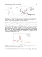
Fig.7 shows the growth distance of the single crystals and mean matrix grain sizes vs.
growth time. For the samples with 0 and 0.5 mol % K
4
CuNb
8
O
23
, crystal growth is initially
rapid but tails off with growth time (Fig.7a). Addition of 0.5 mol % K
4
CuNb
8
O
23
causes a
reduction in single crystal growth distance at all annealing times. For the sample with 2 mol
% K
4
CuNb
8
O
23
, the crystal growth rate decreases after 1 hour and then remains
approximately constant up to 20 h. For the samples with 0 and 0.5 mol % K
4
CuNb
8
O
23
,
matrix grain growth is initially rapid but then tails off with annealing time (Fig.7b). For the
samples with 2 mol % K
4
CuNb
8
O
23
, after initial growth for 1 h, the matrix grain size remains
almost constant up to 20 h.
Fig. 7. (a) growth distance of single crystal and (b) mean matrix grain radius vs. growth time
at 1100°C (Fisher et al., 2008b)
This behaviour is explained by considering the effect of the liquid phase on both single
crystal growth and matrix grain growth. Because the seed crystal acts as a very large grain,
for the single crystal equation [2] can be approximated to:
1
2
sl
Y
r
(5)
Therefore, the single crystal growth rate is inversely proportional to the mean matrix grain
size. In the samples with 0 and 0.5 mol % K
4
CuNb
8
O
23
, matrix grain growth causes the
driving force for single crystal growth to decrease with annealing time and the single crystal
Growth and Characterization of Single Crystals
of Potassium Sodium Niobate by Solid State Crystal Growth
97
growth rate to slow down. Addition of 0.5 mol % K
4
CuNb
8
O
23
liquid phase sintering aid can
further reduce both the crystal and matrix grain growth rates, as the thickness of the
solid/liquid interface across which atoms must diffuse increases (Kang, 2005). With
addition of 2 mol % K
4
CuNb
8
O
23
, matrix grain growth effectively ceases after 1 h. This
means that the driving for single crystal growth remains constant after 1 h, allowing the
crystal to keep growing even for extended annealing times.
Table 1 gives EDXS analyses of single crystals and matrix grains of samples with different
amounts of K
4
CuNb
8
O
23
. Again, single crystals of KNbO
3
and NaNbO
3
were used as
standards. For the samples with 0 and 0.5 mol % K
4
CuNb
8
O
23
, both the single crystal and
matrix grains have compositions close to the nominal composition. For the sample with 2
mol % K
4
CuNb
8
O
23
, the matrix grains have the nominal composition but the single crystal is
Na-rich. According to the KNbO
3
-NaNbO
3
phase diagram, (K
0.5
Na
0.5
)NbO
3
at 1100°C lies
just below the solidus line (Jaffe et al., 1971). It is possible that addition of 2 mol %
K
4
CuNb
8
O
23
lowered the solidus temperature to below 1100°C. This would then cause the
equilibrium solid phase to be Na-rich. Indeed, the growing single crystal is Na-rich. The
matrix grains retain their original composition as their growth rate is very slow. Therefore,
care must be taken when adding a liquid phase sintering aid to promote single crystal
growth in this system.
Amount of K
4
CuNb
8
O
23
(mol %) K (at. %) Na (at. %) K/Na ratio
0 (single crystal) 10.34 ± 0.58 10.82 ± 0.64 0.96 ± 0.04
0 (matrix) 10.64 ± 0.62 10.53 ± 0.58 1.01 ± 0.05
0.5 (single crystal) 10.41 ± 0.44 10.39 ± 0.41 0.99 ± 0.05
0.5 (matrix) 10.48 ± 0.63 10.42 ± 0.96 1.02 ± 0.13
2 (single crystal) 8.46 ± 0.54 13.35 ± 0.65 0.64 ± 0.06
2 (matrix) 10.58 ± 0.32 10.79 ± 0.99 0.99 ± 0.10
Nominal composition for (K
0.5
Na
0.5
)NbO
3
10 10 1
Table 1. EDXS analyses of single crystals and matrix grains of samples annealed at 1100°C
for 10 h (Fisher et al., 2008b).
4.4 Growth of [(K
0.5
Na
0.5
)
0.97
Li
0.03
](Nb
0.8
Ta
0.2
)O
3
single crystals by SSCG.
The SSCG method was successfully applied to the growth of (Li, Ta)-KNN modified
single crystals (Fisher et al., 2007b). Powder of a nominal [(K
0.5
Na
0.5
)
0.97
Li
0.03
](Nb
0.8
Ta
0.2
)O
3
composition was prepared in a similar way as before, but with a higher calcination
temperature of 900°C. 0.5 mol % of K
4
CuNb
8
O
23
was added as a liquid phase sintering
aid. A <001>-oriented KTaO
3
single crystal was used as a seed. The sample was pre-
densified by hot pressing at 975°C / 50 MPa for 2 h. The crystal was grown by annealing
in air at 1135°C for 50 hours under atmospheric pressure. A single crystal 100m thick
grew on the seed (Fig.8). SEM-EDXS analysis showed that the single crystal and the
matrix grains have the same composition; however, it was not possible to analyse Li
content by means of EDXS.
Ferroelectrics – Material Aspects
98
Fig. 8. SEM micrograph of [(K
0.5
Na
0.5
)
0.97
Li
0.03
](Nb
0.8
Ta
0.2
)O
3
Single Crystal grown by SSCG
(Fisher et al., 2007b)
5. Dedicated structural and compositional study of a (K
0.5
Na
0.5
)NbO
3
single
crystal
The studies of structure and composition were performed on the hot-pressed KNN single
crystals (see Fig. 5a). For the single crystal XRD setup, the size of the single crystals after
their removal from the matrix was not sufficient. Therefore, the obtained crystals were
crushed and a powder XRD setup was used.
In Fig. 9, experimental XRD powder diffraction patterns of the crushed KNN single crystal
and a polycrystalline KNN ceramic, as well as calculated a XRD diffraction pattern are
shown. The inset in Fig. 9 shows an enlarged view of the 100/001 and 010 diffraction peaks
for the KNN single crystal and ceramic. Both the single crystal and ceramic have narrow and
well defined peaks. No secondary phases were detected (Benčan et al., 2009). In previous
work, different workers have refined KNN unit cell parameters using perovskite unit cells
with orthorhombic symmetry (Attia et. al., 2005), monoclinic symmetry (Shiratori et. al.,
2005) and also triclinic symmetry (Shiratori et. al., 2005). Our experimental data was fitted
using the monoclinic symmetry given by Tellier et al. (Tellier et al. 2009), with unit cell
parameters a=4.0046Å, b=3.9446 Å, c=4.0020 Å, and β=90.3327º.
A precise chemical analysis of the KNN single crystal was performed by WDXS and semi-
quantitative EDXS analysis in the SEM at twelve selected points across the KNN single
crystal. For WDXS analysis, KNbO
3
and NaNbO
3
single crystals were used as standards.
Table 2 shows the determined elemental composition of the KNN single crystal, which is
very close to the nominal one. The small variations in the values of standard deviation for
both WDXS and EDXS analysis serve as proof of the crystal’s homogeneity. The latter makes
it possible to use these crystals as reference standards for the quantitative analysis of sodium
and potassium in other materials (Benčan et al., 2009).
Growth and Characterization of Single Crystals
of Potassium Sodium Niobate by Solid State Crystal Growth
99
Fig. 9. XRD powder diffraction patterns of the crushed KNN single crystal and
polycrystalline KNN ceramic. A calculated XRD pattern using a monoclinic KNN unit cell is
added (Benčan et al., 2009)
Element Nominal composition WDXS EDXS
at% at% STDEV at% STDEV
K 10 10.06 0.08 9.5 0.1
Na 10 10.03 0.07 9.8 0.2
Nb 20 19.89 0.10 20.3 0.3
O 60 60.02 0.15 60.4* 0.5
Table 2. Elemental composition in at% of the KNN single crystal, determined by WDXS and
EDXS, with standard deviation (STDEV). Nominal composition is shown for comparison.
Oxygen (*) is calculated from the stoichiometry (Benčan et al., 2009)
The domain structure of KNN single crystals at micro- and nano-scales was analysed using
the techniques of optical, scanning and transmission electron microscopy (Benčan et al.,
2009). A polarized light optical micrograph of the KNN single crystal is shown in Fig. 10a.
The crystal is still embedded in the KNN ceramic matrix. Large ferroelectric domains from
50 to 100 microns in size are revealed by dark/bright contrast oscillations in the micrograph.
These large domains in turn contain smaller domains with dimensions from tens of microns
down to hundreds of nm. The smaller domains have a herring bone 90º arrangement, as
shown in the inset. in Fig. 10a. The larger domains in the single crystal were also probed by
electron backscattered diffraction (EBSD). The EBSD image (Fig. 10b) shows the distribution
of the orientations in the crystal and surrounding matrix. Differences in colour inside the
single crystal are attributed to the differently oriented ferroelectric domains. From the
colour-key inverse-pole-figure it can be seen that the orientation inside the single crystal is
Ferroelectrics – Material Aspects
100
changing by 90
o
and that there are three different orientations rotated to each other by 90
o
angles.
Fig. 10. Optical microscope micrographs of the KNN single crystal and its domain
microstructure. The inset shows a herring bone 90º arrangement of smaller domains (a)
EBSD orientation map of the KNN single crystal and the corresponding color-key inverse-
pole-figure (b) (Benčan et al., 2009)
In order to determine the domain structure at the nanometer scale, the specimen was
investigated by TEM (Benčan et al., 2009). Smaller saw-like domains with a size of about
50nm were arranged within the larger ones (Fig.11).
Fig. 11. TEM-BF image of the KNN single crystal with corresponding SAED patterns
showing the presence of 180 º domains. Due to the very small difference in a and c unit cell
parameters, a and c axes were chosen arbitrarily (Benčan et al., 2009)
The overlapping of these domains is represented by the selected area diffraction (SAED)
pattern in the [010] zone axis, taken from the area of ~1.5 μm. Splitting of the {h00} or {00l}
reflections parallel to the <001> or <100> directions is seen. This is due to the β angle (~
90.3º). Such patterns can be experimentally observed only in the case where the [100] or
a)
b)
Growth and Characterization of Single Crystals
of Potassium Sodium Niobate by Solid State Crystal Growth
101
[001] direction of one domain is parallel to the [-100] or [00-1] direction of the other one,
meaning that these are 180º domains.
6. Dielectric, ferroelectric, piezoelectric and electrostrictive properties of
K
0.5
Na
0.5
NbO
3
single crystals
The dielectric properties of a hot-pressed KNN single crystal (see Fig. 5a for reference) were
measured on the as-cut piece of crystal in two perpendicular orientations. These were
determined from EBSD analysis and described as [1
3
1] and the [
323
]. Fig. 12 shows the
temperature dependence of the dielectric constant (ε) and the dielectric losses (tan δ)
measured for the KNN single crystal in the above mentioned directions and also for the
surrounding polycrystalline KNN matrix. The highest value of ε was obtained for the [1
3 1]
direction of the KNN single crystal across whole temperature range. At the same time, two
phase transitions from the monoclinic to the tetragonal phase (T
1
) at around 193°C, and from
the tetragonal to the cubic phase (T
2
) at around 410°C were measured (Ursič et al, 2010). The
latter are in accordance with the transitions observed in the surrounding polycrystalline
KNN ceramic, which is another indication of the obtained crystal compositional
homogeneity. Table 3 summarizes the dielectric properties obtained for the KNN single
crystal in both directions and for the surrounding polycrystalline KNN matrix, and gives a
comparison with the dielectric properties of KNN-based single crystals reported in the
literature.
0 100 200 300 400 500
0
2000
4000
6000
8000
10000
12000
14000
tg
KNN s.c. - [131] direction
KNN s.c. - [323] direction
KNN surrounding ceramics
T (°C)
0.0
0.1
0.2
0.3
0.4
0.5
0.6
0.7
0.8
0.9
1.0
1.1
Fig. 12. Comparison of ε (thick lines) and tanδ (thin lines) as a function of the temperature
for the KNN single crystal in [1
3 1] and the [ 323 ] directions and for KNN surrounding
ceramics measured at 100 kHz (Uršič et al., 2010).
Due to the high dielectric constant, the [1
3 1] direction of KNN single crystal was chosen for
further measurements of the ferroelectric, piezoelectric and electrostrictive properties. The
ferroelectric properties, i.e. the remnant polarization (Pr) and coercive field (Ec) measured
for the KNN single crystal and surrounding polycrystalline KNN matrix, are compared to
the literature and shown in Table 4.
Ferroelectrics – Material Aspects
102
System Freq. (kHz) ε
Troom
tg δ
Troom
T
1
(°C)
T
2
(°C)
KNN s.c. [1 3 1]
this study
100 1015 0.01 192 410
KNN s.c. [ 323 ]
this study
100 650 0.01 193 409
KNN ceramics
this study
100 750 0.01 193 411
K
0.5
Na
0.5
NbO
3
s.c. [001]
Lin et al., 2009
100 240 0.02 205 393
K
0.47
Na
0.53
NbO
3
s.c. [100]
c
Kizaki et al., 2007
1000 600 below 0.1 190 390
K
0.53
Na
0.47
Mg
0.004
Nb
0.996
O
y
s.c.
[100]
c
Kizaki et al., 2007
1000 740 below 0.1 160 390
0.95(K
0.5
Na
0.5
)NbO
3
-0.05LiNbO
3
s.c. [001]
Chen et al., 2007
100 185 0.01 192 426
Li
0.02
(Na
0.5
K
0.5
)
0.98
NbO
3
s.c. [001]
c
Davis et al.,
2007
1 205 0.33 177 /
Table 3. The ε, tgδ and monoclinic - tetragonal (T
1
) and tetragonal - cubic (T
2
) phase
transition temperatures for KNN single crystal in the [1
3 1] and the [ 323 ] directions and for
KNN ceramics. For comparison the dielectric properties obtained on KNN based single
crystals by different groups are added (Uršič et al., 2010)
System
Freq.
(Hz)
P
r
(µC/cm
2
)
E
c
(kV/cm)
KNN s.c. [1
3
1]
this study
50 17 24
KNN ceramics
this study
50 15 24
K
0.47
Na
0.53
NbO
3
s.c. [100]
c
Kizaki et al., 2007
1 / /
K
0.53
Na
0.47
Mg
0.004
Nb
0.996
O
y
s.c. [100]
c
Kizaki et al., 2007
1 40 12
0.95(K
0.5
Na
0.5
)NbO
3
-0.05LiNbO
3
s.c. [001]
Chen et al., 2007
10 9 22
Table 4. Ferroelectric properties of KNN single crystalsin the [1 3 1] direction and for KNN
ceramics. For comparison the ferroelectric properties obtained on KNN based single crystals
by different groups are added (Uršič et al., 2010)
The displacement signal versus the applied voltage of the KNN single crystal in the [1
3 1]
direction and of the surrounding KNN ceramic were measured using an atomic force
microscope (AFM). Prior to the analysis, an AFM measurement was performed as a
reference on glass under the same experimental conditions as used for the KNN single
crystal and ceramics. No strain was observed for the non-piezoelectric glass, confirming that
strains observed during AFM analysis of the KNN crystal and ceramics are piezoelectric in
nature. The KNN single crystals were not poled before the AFM measurement.
The obtained displacement signal consists of two components. The first component has the
same frequency as the applied voltage, i.e., this is the linear piezoelectric component (see
Fig. 13). The second component is the pronounced quadratic component with the double
frequency (see inset in Fig. 14). The piezoelectric coefficients d
33
, shown in Fig. 13, were
determined from the slopes of the linear fits of the linear component of displacement versus
the applied voltage (Uršič et al., 2010).
The d
33
piezoelectric coefficients for the KNN single crystal and for the surrounding ceramic
are approximately 80 pm/V at a measurement frequency of 2 Hz. As frequency increases,
Growth and Characterization of Single Crystals
of Potassium Sodium Niobate by Solid State Crystal Growth
103
the d
33
value for the KNN single crystal decreases (see Fig.13). Although very small applied
electric fields (up to 0.1 kV/mm) were used to measure the piezoelectric coefficient for the
KNN single crystal, the obtained d
33
value (80 pm/V) was in the same range as for the poled
KNN ceramic. The explanation of such behaviour can be given by the domain structure of
the KNN single crystal. As shown in Section 5 the KNN single crystal consists of large 90°
domains with widths of up to 100 microns, and smaller 180° domains with widths ranging
between a few tens of nms to 300 nm. Since the contact area of the AFM tip is around 20 nm,
it is likely that only the smaller 180° domain walls are moving during the AFM
measurements. These small 180° domains probably contribute to the obtained linear
response of the KNN single crystal. The inability of the 180° domains to reorientate quickly
enough at higher frequencies explains the decrease in d
33
with increasing measurement
frequency. It has been previously demonstrated by McKinstry et al. (McKinstry et al., 2006)
that if the mobility of 90
o
domains is limited, then the 180° domains can contribute to the
piezoelectric linear response.
0 20 40 60 80 100 120 140
0
2
4
6
8
10
12
d
33
ceram.
=78 pm/V
d
33
s.c.
= 67 pm/V
d
33
s.c.
=40 pm/V
Displacement (nm)
Voltage (V)
2 Hz s.c.
Fit of data at 2 Hz
20 Hz s.c.
Fit of data at 20 Hz
200 Hz s.c.
Fit of data at 200 Hz
2 Hz ceramics
Fit of data for ceramics
d
33
s.c.
=79 pm/V
Fig. 13. The linear part of displacement versus voltage amplitude of KNN single crystal in [1
3 1] direction measured at 2 Hz, 20 Hz and 200 Hz. The measurement for KNN surrounding
ceramics at 2 Hz is added for comparison (Uršič et al., 2010)
The electrostrictive coefficients (M
33
) were determined from the slope of the linear fit of the
relative strain versus the square of the amplitude of the electric field, as shown in Fig. 14.
The M
33
for the surrounding KNN ceramic was lower than that of the KNN single crystal.
The measured values M
33
for the KNN single crystal are significantly higher than values of
M
33
for PMN-based single crystals. The highest obtained electrostrictive coefficient for a
0.65Pb(Mg
1/3
Nb
2/3
)O
3
-0.35PbTiO
3
single crystal was in the range 1.3 to 4x10
-15
m
2
/V
2
at 0.01
Hz; a 90
o
domain wall contribution to electrostriction was reported (Bokov&Ye, 2002). Such
a high M
33
value for the KNN single crystal can arise from the intrinsic electrostrictive
behaviour as well as the extrinsic contribution, i.e., the strain from the domain-wall motion.
Most probably in the KNN single crystal, the main contribution to electrostrictive strain
arises from the contribution of 180° domain walls. Our results agree with the findings
obtained by McKinstry et al. (McKinstry et al., 2006), who showed that 180° domains walls
Ferroelectrics – Material Aspects
104
can contribute to the linear response as well as to electrostrictive strain response in
ferroelectric materials. Although the pure electrostrictive response should be frequency
independent, they observed in (111) Pb(Zr
0.45
Ti
0.55
)O
3
thin films a decrease of the second-
order strain with frequency by 20%, as was also the case for our KNN single crystal.
0.00E+000 8.00E+008 1.60E+009 2.40E+009 3.20E+009
0.00000
0.00001
0.00002
0.00003
0.00004
0.00005
0.00006
0.00007
0.00008
0 10203040506070
0
20
40
60
80
100
M
33
cer.
=1.58 10
-14
m
2
/V
2
M
33
=2.39 10
-14
m
2
/V
2
M
33
=2.08 10
-14
m
2
/V
2
M
33
=2.59 10
-14
m
2
/V
2
2 Hz s.c.
Fit of data at 2 Hz
20 Hz s.c.
Fit of data at 20 Hz
200 Hz s.c.
Fit of data at 200 Hz
2 Hz ceramics
Fit of data for ceramics
E
2
0
(V
2
/m
2
)
Displacement (nm)
Voltage (V)
Strain (relative strain)
Fig. 14. Relative strain versus square of the amplitude of the electric field of KNN single
crystal in the [1
3 1] direction at 2 Hz, 20 Hz and 200 Hz. Inset shows the quadratic part of
displacement versus voltage for KNN single crystal. The measurement for KNN
surrounding ceramics at 2 Hz is added for comparison (Uršič et al., 2010)
7. Conclusions
In this chapter the principles of the SSCG technique and its application to the growth of
K
0.5
Na
0.5
NbO
3
(KNN) and Li,Ta-modified KNN single crystals were presented. With the use
of the complementary analytical characterization techniques, i.e. XRD, optical microscopy
and electron microscopy (SEM, EDXS, WDXS, EBSD, TEM, SAED), the precise
compositional and structural analysis of KNN single crystals was performed and the
correlation with its electrical properties was given.
There are several possible directions for future work. First, it would be useful to grow larger
single crystals. This will enable crystals to be cut in controlled orientations e.g along the
[001] or [110] directions and their properties measured and compared with KNN crystals
grown by solution-based methods. Furthermore, alternative seed crystals need to be found.
Although KTaO
3
single crystals make excellent seeds, they are rather expensive and to grow
large single crystals, large seed crystals are needed. If cheaper alternatives could be found,
this would reduce the cost of growing large KNN single crystals. Work needs to be done in
growing single crystals from seeds placed on top of the ceramic substrate. Finally, growth of
other compositions such as Li-doped KNN should be carried out.
Growth and Characterization of Single Crystals
of Potassium Sodium Niobate by Solid State Crystal Growth
105
8. Acknowledgments
Dr. Daniel Rytz, from FEE GmbH, Germany is acknowledged for the preparation of KTaO
3
seeds. The authors wish to acknowledge the financial support of the Slovenian Research
Agency (P2-105) and the 6FP project IMMEDIATE.
9. References
Arndt, U.W. & Willis, B.T.M. (1966).Single Crystal Diffractometry (1
st
edition), Cambridge
University Press, ISBN:978-0-521-04060-0, New York
Attia, J., Bellaiche, M., Gemeiner, P., Dkhil, B. & Malič, B. (2005). Study of potassium-
sodium-niobate alloys: A combined experimental and theoretical approach.
Journal
de Physique IV (Proceedings), Vol. 128, No.1, (September 2005), pp. 55–60, ISSN:1155-
4339
Bauser, E. & Strunk, H. (1982).Dislocations as Growth Step Sources in Solution Growth and
Their Influence on Interface Structure.
Thin Solid Films, Vol. 93, Nos. 1-2, (July 1982),
pp. 185-94,ISSN:0040-6090
Benčan, A., Tchernychova, E., Godec, M., Fisher, J. & Kosec M. (2009).Compositional and
Structural Study of a (K
0.5
Na
0.5
)NbO
3
Single Crystal Prepared by Solid State Crystal
Growth.
Microscopy and Microanalysis, Vol.15, No.5, (October 2009), pp. 435-440,
ISSN:1431-9276
Benčan, A., Tchernychova, E., Šturm, S., Samardzija, Z., Malič, B. & Kosec, M. (2011).
Approches for a reliable compositional analysis of alkaline-based lead-free
perovskite ceramics using microanalytical methods.
Journal of Advanced
Dielectrics,Vol.1, No.1, (January 2011), pp. 41-52, ISSN:2010-1368
Bennema P. (1993). Growth and Morphology of Crystals. In:Handbook of Crystal Growth 1
Fundamentals Part A: Thermodynamics and Kinetics, D. T. J. Hurle (Ed.), pp. 481–
581,ISBN: 0444889086, North-Holland, Amsterdam
Bokov, A. & Ye, Z. G. (2002). Giant electrostriction and stretched exponential
electromechanical relaxation in 0.65Pb(Mg
1/3
Nb
2/3
)O
3
-0.35PbTiO
3
crystals, Journal
of Applied Physics, Vol. 91,No. 10 (May 2002),pp. 6656- 6661, ISSN:0021-8979
Bomlai, P.,Wichianrat, P.,Muensit, S. & Milne, S.J. (2007). Effect of Calcination Conditions
and Excess Alkali Carbonate on the Phase Formation and Particle Morphology of
Na
0.5
K
0.5
NbO
3
Powders. Journal of American Ceramic Society,Vol. 90, No. 5, (May
2007),pp. 1650-1655, ISSN:0002-7820
Burton, W. K., Cabrera, N. & Frank, F. C. (1951). The Growth of Crystals and the
Equilibrium Structure of Their Surfaces.
Philosophical Transactions of the Royal Society
of London Series A, Vol. 243, (June 1951), pp.299-358, ISSN: 0962-8428
Chen, K., Xu, G., Yang, D. ,Wang, X. & Li J. (2007). Dielectric and piezoelectric properties of
lead-free 0.95(K
0.5
Na
0.5
)NbO
3
–0.05LiNbO
3
crystals grown by the Bridgman method.
Journal of Applied Physics,Vol. 101,No. 4, (February 2007), pp. 0441031-4,ISSN:0021-
8979
Chiang, Y. M., Birnie III, D. & Kingery, W. D. (1997).
Physical Ceramics: Principles for Ceramic
Science and Engineering, John Wiley & Sons, Inc., ISBN 0-471-59873-9, New York
Choi, J.J., Ryu, J. & Kim, H. E. (2001). Microstructural Evolution of Transparent PLZT
Ceramics Sintered in Air and Oxygen Atmospheres.
Journal of the American Ceramic
Societ,.Vol. 84, No. 7 (July 2001), pp. 1465-1469, ISSN:0002-7820
Ferroelectrics – Material Aspects
106
Davis, M., Klein, N.,Damjanovič, D. & Setter, N. (2007). Large and stable thickness coupling
coefficients of [001]
c
oriented KNbO
3
and Li-modified (K,Na)NbO
3
single crystals.
Applied Physics Letters.Vol. 90, No. 6 (February 2007), pp.062904 1-3,ISSN:0003-6951
DeVries.R.C. (1964). Growth of Single Crystals of BaTiO
3
by Exaggerated Grain
Growth.
Journal of the American Ceramic Society, Vol. 47, No. 3 (March 1964), pp. 134-
136,ISSN:0002-7820
Fisher, J. G., Benčan, A., Holc, J., Kosec, M., Vernay, S. & Rytz, D. (2007a). Growth of
Potassium Sodium Niobate Single Crystals by Solid State Crystal Growth.
Journal of
Crystal Growth, Vol. 303, No. 2 (May, 2007), pp. 487-492, ISSN:0022-0248
Fisher, J. G., Benčan, A., Bernard, J., Holc, J., Kosec, M., Vernay, S. & Rytz, D. (2007b).
Growth of (Na,K,Li)(Nb,Ta)O
3
Single Crystals by Solid State Crystal Growth.
Journal of the European Ceramic Society, Vol. 27, Nos. 13-15 (2007), pp. 4103-
4106,ISSN:0955-2219
Fisher, J. G., Benčan, A., Kosec, M., Vernay, S. & Rytz, D. (2008a).Growth of Dense Single
Crystals of Potassium Sodium niobate by a Combination of Solid-State Crystal
Growth and Hot Pressing.
Journal of the American Ceramic Society, Vol. 91, No. 5
(May 2008), pp. 1503-1507,ISSN:0002-7820
Fisher, J. G., Benčan, A., Godnjavec, J. & Kosec, M. (2008b). Growth Behaviour of Potassium
Sodium Niobate Single Crystals Grown by Solid-State Crystal Growth Using
K
4
CuNb
8
O
23
as a Sintering Aid. Journal of the European Ceramic Society, Vol. 28, No.
8 (2008), pp. 1657-1663,ISSN:0955-2219
Goldstein, J., Lyman, C.E., Newbury, D.E.,Lifshin, E., Echlin, P., Sawyer, L., Joy D.C. &
Michael, J.R. (2003).
Scanning Electron Microscopy and X-Ray Microanalysis, (3
rd
edition), Kluwer Academic and Plenum Publishers, ISBN:0-306-47292-9, New York
Gorzkowski, E. P., Chan, H. M. & Harmer, M. P. Effect of PbO on the Kinetics of {001}
Pb(Mg
1/3
Nb
2/3
)O
3
- 35mol%PbTiO
3
Single Crystals Grown into Fully Dense
Matrices.
Journal of the American Ceramic Society, Vol.89, No.3, (March 2006) pp. 856-
862,ISSN:0002-7820
Greenwood, G. W. (1956). The Growth of Dispersed Precipitates in Solutions.
ActaMetallurgica,Vol. 4, No. 3 (May 1956), pp. 243-348, ISSN:0001-6160
Hennings, D. F. K., Janssen, R. & Reynen, P. J. L. (1987). Control of Liquid-Phase- Enhanced
Discontinuous Grain Growth in Barium Titanate.
Journal of the American Ceramic
Society, Vol. 70, No. 1 (January 1987), pp.23-27,ISSN:0002-7820
Hirth, J. P. & Pound, G.M. (1963). Condensation and Evaporation.
Progress in Materials
Science.Vol. 11, (1963), pp. 17-192,ISSN:0079-6425
Jaffe, B., Cook Jr., W. R. & Jaffe, H. (1971). Perovskite niobates and tantalates and other
ferroelectric and antiferroelectric perovskites, In:
Piezoelectric Ceramics, Eds.
J.P.Roberts & P.Popper, Academic Press, pp. 185-212, ISBN 0123795508, London
Jenko, D., Benčan, A., Malič, B., Holc, J. & Kosec, M. (2005). Electron microscopy studies of
potassium sodium niobate ceramics.
Microscopy and microanalysis, Vol. 11, No.6
(December 2005), pp. 572-580, ISSN:1435-8115
Kang, S. J. L. & Yoon, K. J. (1989). Densification of Ceramics Containing Entrapped Gases.
Journal of the European Ceramic Society, Vol. 5, No. 2 (1989), pp. 135-139, ISSN:0955-
2219
Kang, S. J. L. (2005). Chapter 15, Grain Shape and Grain Growth in a Liquid Matrix, In:
Sintering: Densification, Grain Growth and Microstructure, pp. 205-26, Elsevier,
ISBN:07506 63855, Oxford
Khan, A., Meschke, F. A., Li, T., Scotch, A. M., Chan, H. M. & Harmer, M. P. (1999). Growth
of Pb(Mg
1/3
Pb
2/3
)O
3
– 35 mol% PbTiO
3
Single Crystals from (111) Substrates by
Growth and Characterization of Single Crystals
of Potassium Sodium Niobate by Solid State Crystal Growth
107
Seeded Polycrystal Conversion.Journal of the American Ceramic Society,Vol. 82,
No.11, (November 1999), pp. 2958-62,ISSN:0002-7820
Kim, M. S., Fisher, J. G., Kang, S. J. L. & Lee, H. Y. (2006). Grain Growth Control and Solid-
State Crystal Growth by Li
2
O/PbO Addition and Dislocation Introduction in the
PMN-35 PT System.
Journal of the American Ceramic Society, Vol. 89, No. 4 (April
2006), pp. 1237–1243,ISSN:0002-7820
Kizaki, Y., Noguchi, Y. & Miyayama, M. (2007). Defect control for Superior Properties in
K
0.5
Na
0.5
NbO
3
Single Crystals. Key Engineering Materials, Vol. 350, (October 2007),
pp. 85-88, ISSN:1013-9826
Kosec, M., Malič, B., Benčan, A. & Rojac, T. (2008). KNN-based piezoelectric ceramics.
In:
Piezoelectric and Acoustic Materials for Transducer Applications,Eds.: A. Safari and
E. K. Akdogan,pp. 81-102, Springer, ISBN: 978-0-387-76538-9., New York
Kosec, M., Malič, B., Benčan, A., Rojac, T. & Tellier, J. (2010). Alkaline niobate-based
piezoceramics: crystal structure, synthesis, sintering and microstructure.
Functional
materials letters Vol. 3, No.1, (March 2010), pp. 15-18, ISSN:1793-6047
Kosec, M. &Kolar, D. (1975).On Activated Sintering and Electrical Properties of NaKNbO
3
.
Material Research Bulletin, Vol. 10, No. 5, (May 1975), pp. 335–40,ISSN: 0025-5408
Kugimiya, K., Hirota, K. & Matsuyama, K. (1990). Process for Producing Single Crystal
Ceramics. US Pat. No. 4900393, 1990.
Kwon, S. K., Hong, S. H., Kim, D. Y. & Hwang, N. M. (2000). Coarsening Behavior of
Tricalcium Silicate (C
3
S) and Dicalcium Silicate (C
2
S) Grains Dispersed in a Clinker
Melt.
Journal of the American Ceramic Society, Vol. 83, No. 5, (May 2000), pp. 1247-
1252,ISSN:0002-7820
Lee, B. K., Chung, S. Y. & Kang, S. J. L. (2000). Grain Boundary Faceting and Abnormal
Grain Growth in BaTiO
3
. Acta Materialia, Vol. 48, No. 7, (April 2000), pp. 1575-
1580ISSN:1359-6454
Lee H. Y. (2003). Solid-State Single Crystal Growth (SSCG) Method: A Cost-effective Way of
Growing Piezoelectric Single Crystals. In: P
iezoelectric Single Crystals and their
Applications, S. Trolier-McKinstry, L. E. Cross and Y. Yamashita (Eds.), pp. 160-177,
Pennsylvania State University, State College, PA
Lin, D., Li, Z., Zhang, S., Xu Z. & Yao, X. (2009). Dielectric/piezoelectric properties and
temperature dependence of domain structure evolution in lead free K
0.5
Na
0.5
/NbO
3
single crystal. Solid State Communications, Vol. 149, No.39-40, (October 2009), pp.
1646- 1649, ISSN:0038-1098
Malič, B., Benčan, A., Rojac, T. & Kosec, M. (2008a). Lead-free Piezoelectrics Based on
Alkaline Niobates: Synthesis, Sintering and Microstructure.
Acta Chimica Slovenica,
Vol. 55, No.4, (December 2008),pp. 709-718, ISSN: 1318-0207
Malič, B., Jenko, D., Holc, J., Hrovat, M. & Kosec, M. (2008b). Synthesis of sodium potassium
niobate: a diffusion couples study
. Journal of the American Ceramic Society, Vol. 91,
No.6, pp. 1916-1922, ISSN: 0002-7820
Matsubara, M., Yamaguchi, T., Sakamoto, W., Kikuta K., Yogo, T. & Hirano, S. I. (2005).
Processing and Piezoelectric Properties of Lead-Free (K,Na)(Nb,Ta)O
3
Ceramics.
Journal of the American Ceramic Society, Vol. 88, No. 5, (May 2005), pp. 1190-
1196,ISSN:0002-7820
McKinstry, T. S., Gharb N. B. & Damjanovic, D. (2006). Piezoelectric nonlinearity due to
motion of 180°domain walls at subcoercive fields: A dynamic poling model.
Applied
Physics Letters, Vol. 88, No.20, (May 2006) pp. 202901-3, ISSN:0003-6951
Ferroelectrics – Material Aspects
108
Park, S.E. & Shrout, T.R. (1997). Ultrahigh strain and piezoelectric behavior in relaxor based
ferroelectric single crystals.
Journal of Applied Physics, Vol. 82, No.4, (August 1997)
pp. 1804-1811,ISSN:0021-8979
Rehrig, P. W., Park, S. E., Trolier-McKinstry, S., Messing, G. L., Jones, B. & Shrout, T.
R.(1999). Piezoelectric Properties of Zirconium-doped Barium Tiotanate Single
Crystals Grown by Templated Grain Growth.
Journal of Applied Physics, Vol. 86,
No.3 (August 1999), pp. 1657-1661, ISSN:0021-8979
Rödel, J., Jo, W., Seifert, K., Anton, E. M., Granzow, T. & Damjanovič, D. (2009). Perspective
on the Development of Lead-free Piezoceramics,
Journal of the American Ceramic
Society, Vol. 92, No.6, (June 2009), pp. 1153- 1177, ISSN:0002-7820
Saito, Y., Takao, H., Tani, T., Nonoyama, T., Takatori, K., Homma, T., Nagaya, T. &
Nakamura, M., (2004). Lead-free piezoceramics,
Nature, Vol. 432, No. 7013, pp. 84-
87 (November 2004), ISSN: 0028-0836
Samardžija, Z., Bernik, S., Marinenko, R. B., Malič, B. & Čeh, M. (2004). An EPMA Study on
KNbO
3
and NaNbO
3
Single Crystals–Potential Reference Materials for Quantitative
Microanalysis.
Microchimica Acta, Vol. 145, Nos. 1-4, (2004), pp. 203–208, ISSN:0026-
3672
Seo, C. E. & Yoon, D. Y. (2005).The Effect of MgO Addition on Grain Growth in PMN-
35PT.
Journal of the American Ceramic Society, Vol. 88, No. 4, (April 2005), pp. 963-967,
ISSN:0002-7820
Shiratori, Y., Magrez, A. & Pithan C. (2005). Particle Size Effect on the Crystal Structure
Symmetry of K
0.5
Na
0.5
NbO
3.
Journal of the European Ceramic Society, Vol. 25, No. 12
(2005), pp. 2075-2079, ISSN:0955-2219
Tellier, J., Malič, B., Dkhil, B., Jenko, D., Cilensek, J. & Kosec, M. (2009). Crystal structure and
phase transition of sodium potassium niobateperovskite.
Solid State Science,Vol. 11,
No. , (February 2009),pp. 320–324, ISSN:1293-2558
Uršič, H., Benčan, A., Škarabot, M., Godec, M. & Kosec, M. (2010). Dielectric, ferroelectric,
piezoelectric, and electrostrictive properties of K
0.5
Na
0.5
NbO
3
single crystals. Journal
of Applied Physics, Vol.107, No. 3, (February 2010), pp. 033705-5, ISSN:0021-8979
van der Eerden, J. P. (1993). Crystal Growth Mechanisms, In:
Handbook of Crystal Growth. 1
Fundamentals Part A: Thermodynamics and Kinetics, D. T. J. Hurle (Ed.), pp. 311-475,
North-Holland, ISBN: 2- 88074-246-3, Amsterdam
Wada, S., Muraoka, K., Kakemoto, H., Tsurumi, T. & Kumagai, H. (2004). Enhanced
Piezoelectric Properties of Potassium Niobate Single Crystals by Domain
Engineering.
Japanese Journal of Applied Physics, Vol.43, No. 9B, (September 2004)
pp.6692-6700, ISSN:0021-4922
Yamamoto, T. & Sakuma, T. (1994). Fabrication of Barium Titanate Single Crystals by Solid-
State Grain growth.
Journal of the American Ceramic Society, Vol. 77, No. 4, (April
1994), pp.1107-1109, ISSN:0002-7820
Yoon, D.Y., Park, C.W.& Koo, J.B. (2001).The Step Growth Hypothesis for Abnormal Grain
Growth.In:
Ceramic Interfaces 2, S.J.L. Kang (Ed.), pp. 2-21, Institute of Materials,
ISBN:978 1 861251 18 3, London
Zhang, S., Lee, S. M., Kim, D. H., Lee, H. Y. & Shrout, T. R. (2007). Electromechanical
Properties of PMN–PZT Piezoelectric Single Crystals NearMorphotropic Phase
Boundary Compositions.
Journal of the American Ceramic Society Vol. 90, No. 12
(December 2007), pp.3859-3862,ISSN:0002-7820
6
Deposition of CoFe
2
O
4
Composite
Thick Films and Their Magnetic,
Electrical Properties Characterizations
W. Chen and W. Zhu
Microelectronics Center, School of Electrical and Electronic Engineering,
Technological University Nanyang
Singapore
1. Introduction
In recent years, spinel ferrites have been shown to exhibit interesting electrical conductivity
and dielectric properties in their nanocrystalline form compared with that of the micrometer
size grains (Ponpandian & Narayanasamy, 2002; Sepelak et al., 2000; Dias & Moreira, 1999).
Typical examples of Ni-Zn ferrites and Co-ferrites have been extensively investigated: the
former suggests that dielectric constant of nanostructured Ni-Zn ferrite is smaller than that
of bulk ceramics (Sivakumar et al., 2008), but the situation is reversed for the Co-ferrites
(Sivakumar et al., 2007). Fortunately the dielectric loss of nanostructured ferrites is hence
reduced for both of them compared to their bulks. Furthermore, a non-Debye type of
dielectric relaxation is observed in these ferrites, which is extensively expressed by electrical
modulus (Sivakumar et al., 2008; Sivakumar et al., 2007; Perron et al., 2007). However, the
detailed reports on cobalt ferrite, which is one of the potential candidates for magnetic and
magneto-optical recording media (Kitamoto et al., 1999; Fontijin et al., 1999), have not drawn
enough interests so far. Much attention has been paid on the synthesis of nanostructured
cobalt ferrite particles as well as bulk ceramics or thin films (Toksha et al., 2008; Komarneni
et al., 1998; Sathaye et al., 2003; Paike et al., 2007; Bhame & Joy, 2008; Gul et al., 2008) and
characterizations of their magnetic properties. As for their dielectric properties, which can
provide important information on the behavior of localized electric charge carriers, giving
rise to a better understanding of the mechanism of dielectric polarization, have attracted
little attention except few reports on nanostructured CoFe
2
O
4
powder (Sivakumar et al.,
2007; George et al., 2007). Recently, more attention has been paid to the electric properties of
the double-phase multiferroic composites, such as CFO-PZT, and CFO-BTO (Chen et al.,
2010; Zhong et al., 2009), or its doping systems (Gul et al., 2007). While pure CoFe
2
O
4
,
especially its thick film structure, which is a critical scale range for micro-electro-mechanical
systems (MEMS) design, has not been found in the literatures.
In order to explore the processing of cobalt ferrite thick film and its electrical properties for
potential MEMS development, the present work has adopted a similar fabrication to typical
PZT ferroelectric thick films (Chen et al., 2009). 10 µm of cobalt ferrite composite thick films
is successfully prepared via a hybridized sol-gel processing. The influence of annealing
temperature on the phase structures, microstructures, Raman shift, magnetic and electrical
Ferroelectrics – Material Aspects
110
properties are well characterized. Furthermore, Ac conductivity spectra analysis is
employed to investigate the ion motion nature of CoFe
2
O
4
composite thick films. The
detailed electrical investigations were conducted in the frequency range of 100 Hz-1MHz
and temperature range between 25 and 200
o
C. Real and imaginary parts of impedance (Z’
and Z’’) in the above frequency and temperature domain suggested the coexistence of two
relaxation regimes: one was induced by electrode polarization; while the other was
attributed to the co-effect of grains and grain boundaries, which was totally different from
its counterpart of bulks and also not reported in other ferrites. Electrical modulus (M’ and
M’’) further showed the crossover from grains effect to grain boundaries effect with
increasing measured temperature under the suppression of electrode polarization. A non-
Debye relaxation behavior and two segments of frequency independent conductivity were
observed in dielectric spectra, which was also consistent with the results of ac conductivity
spectra. In the conductivity spectra, double power law and single power law were
separately applied to the co-effect from grains and grain boundaries and electrode
polarization effect. Moreover, the dc conductivity from both effects well obeyed the
Arrhenius law and their activation energies were matching to the ones calculated from
imaginary impedance peaks, the detailed physical mechanisms on them were finally
discussed.
2. Deposition of CoFe
2
O
4
composite thick films
2.1 Experimental procedural
CoFe
2
O
4
(abbreviated as CFO) sol-gel solution was prepared by mixing cobalt acetate, ferric
nitrate, and polyvinylpyrrolidone together at 60
o
C according to the molar ratio of 1: 2: 2 till
a clear solution was obtained. Then 40 ml of 2-methoxyethanol was added to get 0.125 M of
CFO sol-gel solution. The pH value of resultant dark-red CFO sol-gel solution was 4.2. In
addition, modified CFO particles were prepared by a high energy ball milling method as
reported previously (Chen et al., 2009), which showed an average particle size of 233 nm.
Next, the modified CFO particles were dispersed in the CFO solution with a mass ratio of
2:3, which is similar to the fabrication of hybridized PZT slurry (Chen et al., 2010), to get the
uniform CFO slurry via an agate ball milling for 15 hours. The collected CFO slurry showed
a black color and was immediately spin coated onto the Pt/Ti/SiO
2
/Si substrate
alternatively with CFO sol-gel solution to obtain the dense CFO film. After each coating
layer, the film was baked at 140
o
C for 3 minutes to dry the solvent and then held at 300
o
C
for another 3 minutes to burn up the organic components. The resulting thick films were
annealed in air at various temperatures from 550
o
C to 700
o
C for 1 hour each, and their
thicknesses were measured via a surface profiler to be around 10 µm.
TGA and DTA were performed using a Thermal Analyzer (TA-60WS) with a heating rate of
2
o
C/min. Phase structures were evaluated using an X-ray diffractometer (2400, Rigaku,
CuK
radiation). Raman spectroscopic measurements were carried out with a WITEC
CRM200 confocal Raman system. The excitation source is 532 nm laser (2.33 eV). Surface
and cross-sectional morphologies of the thick films were obtained using a Scanning Electron
Microscope (JSM-5600LV). Magnetic properties were detected by a Lakeshore Vibration
Sample Magnetometer (7404). After deposition of gold top electrodes with the size of 0.8
mm × 0.8 mm on the surface of thick films using E-beam, impedance spectroscopy was
measured by using a Solartron SI1260 impedance/gain-phase analyzer from 0.1 Hz to 1
MHz at room temperature. In addition, the detailed electrical properties of the thick films
Deposition of CoFe
2
O
4
Composite
Thick Films and Their Magnetic, Electrical Properties Characterizations
111
were measured by an Agilent 4294A precision impedance analyzer over 100 Hz-1MHz and
25-200
o
C at the ac oscillation level of 100 mV. Each measured temperature was kept
constant with an accuracy of ±1
o
C.
2.2 Characterizations
TGA/DTA analysis of the dried CFO slurry, dried at 110
o
C for 24 hours, is shown in Fig. 1.
Fig. 1. DTA/TGA curves of the dried CFO slurry.
TGA yields a weight loss of 21 wt% before 300
o
C, and then nearly keeps stable until 800
o
C.
In the DTA curve, two exothermic peaks are observed: one at 126
o
C which is due to the
organic solvent evaporation; the other at 300
o
C symbols the decomposition and combustion
of the bound organic species in the CFO slurry. Since that the CFO powder has been
presintered at a high temperature of 1200
o
C before high energy ball milling, it has almost
no effect on TGA/DTA analysis. The observations of weight loss and exothermic peak in
DTG can be presumed to be occurring from the sol-gel part of the composite film. That is
why 140
o
C and 300
o
C are selected after each coating processing.
X-ray diffraction patterns of the resultant CFO thick films annealed at different
temperatures are exhibited in Fig. 2.
Fig. 2. XRD patterns of CFO composite thick films annealed at different temperatures.
Although major peaks due to CoFe
2
O
4
are observed for the film annealed at 550
o
C,
additional peaks (marked) assignable to Fe
2
O
3
are also observed indicating the process of
Ferroelectrics – Material Aspects
112
CFO formation is not complete. With the rise of the annealing temperature, complete
formation of spinel phase is observed for films annealed above 600
o
C. Furthermore, these
characteristic peaks of CFO phase become narrow, indicative of an increase of their grain
size with increasing annealing temperature.
In order to further verify the chemical impurity in the composite thick films, micro-Raman
spectroscopy is performed in Fig. 3.
Fig. 3. Micro-Raman spectra of CFO composite thick films annealed at different
temperatures.
It can be seen that three main peaks (298 cm
-1
, 459 cm
-1
, and 677 cm
-1
) of the spinel CFO are
clearly observed for all the films without any Raman shift (Ortega et al., 2008; Yu et al.,
2002).
Films annealed below 600
o
C show the presence of a peak at 600 cm
-1
, which can be
assigned to CFO, supporting the inference that below 600
o
C, formation of CFO does not go
to completion.
In addition, these mode peaks are gradually becoming sharp with the rise of
annealing temperature, suggesting a harden process of CFO modes.
Typical surface morphology and cross-sectional picture of CFO composite thick film
annealed at 700
o
C are shown in Fig. 4.
Fig. 4. Typical surface morphology (a) and cross-sectional image (b) of CFO composite thick
films annealed at 700
o
C.
Deposition of CoFe
2
O
4
Composite
Thick Films and Their Magnetic, Electrical Properties Characterizations
113
It can be seen from Fig. 4(a) that the thick films have rough, dense microstructure due to
agglomeration as is the case for synthesized CFO thin films reported in the literature
(Pramanik et al., 2005). The roughness can be attributed to the overlarge thickness,
evidenced by its cross-sectional picture in Fig. 4(b), which also indicates a thickness closing
to 10 µm. It is far beyond the currently reported ferrite films (Sathaye et al., 2003; Gul &
Maqsood, 2008).
In-plane magnetic hysteresis loops are shown in Fig. 5.
Fig. 5. Magnetic hysteresis loops of CFO composite thick films annealed at different
temperatures.
It can be seen that all the films reach saturation below 8 kOe due to the CFO ferrite thick
film being in a quasi-free state with negligible shear stress from the substrate compared to
chemical synthesized CFO thin film (Sathaye et al., 2003) or pulse laser deposited CFO
epitaxial thin film (Lisfi & Williams, 2003). Furthermore, the present composite thick films
show an annealing temperature dependent saturation magnetization (Ms) and magnetic
coercivity (Hc). With increasing annealing temperature, both Ms and Hc values exhibit a
monotone enhancement. The enhanced Ms values from 79 to 225 emu/cm
3
are due to the
enlargement of average cobalt ferrite grains, which has been demonstrated in CFO bulks
and thin films (Sathaye et al., 2003; Wang et al., 2008). In the CFO thin films (Sathaye et al.,
2003), the Ms value was reported as 300 emu/cm
3
. Compared with the present composite
thick films, the higher Ms value in CFO thin film was mainly caused by higher annealing
temperature.
The particles used in CFO composite thick films include two parts: one is the sol-gel
synthesized particles with a small particle size of dozens of nanometer; the other is high
energy ball milling modified CFO particles with a large average particle size of about 233
nm. Since the latter has been presintered at 1200
o
C, the growth rates of both kinds of CFO
particles under 700
o
C of annealing temperature are different, resulting in non-uniform
segregation causing the rough surface, which increases the coercivity of CFO composite
thick films from 1130 to 1434 Oe. Generally speaking, high coercivity can be obtained in
systems with a nanostructure or preferred orientation, such as thin films with preferred
crystal texture or nanoparticles with a single domain diameter (Yin et al., 2006; Lee et al.,
1998). The single domain diameter of the present CFO is about 40 nm, which is much
smaller than the average diameters of our CFO composite thick films (above 100 nm), plus
Ferroelectrics – Material Aspects
114
the polycrystalline state of the present thick films, evidenced by X-ray diffraction. Thus, the
lower Hc value is mainly attributed to the magnetic multi-domain configuration of the CFO
particles in the composites (Lee et al., 1998).
Room temperature impedance spectroscopy for the CFO composite thick films is exhibited
in Fig. 6 for frequencies of 0.1 Hz to 1 MHz.
Fig. 6. Frequency dependence of real (a) and imaginary impedance (b) of CFO composite
thick films at room temperature from 0.1 Hz to 1 MHz.
Fig. 6(a) shows the frequency dependence of impedance real part (Z’). A step-like
decreasing trend is observed in real impedance spectra for all the samples from 10 Hz to 10
kHz, and their specific impedance values are reduced by nearly three orders of magnitude.
An apparent imaginary impedance peak appears in all the samples and becomes strong
with increasing annealing temperature, as can be seen in Fig. 6(b). It can be seen that the
peak frequency is around 100 Hz, which is in the middle point of the step-like decreasing
curve in real impedance spectra, indicative of a relaxation behavior. This phenomenon has
not been reported in the literatures on CFO ferrite but recent studies on multiferroic BiFeO
3
thin films and BiFeO
3
/CoFe
2
O
4
bilayered thin films show a similar behavior (Srivastava et
al., 2009; Wu & Wang, 2009). The relaxation peak was initially observed in BiFeO
3
thin films
at 150
o
C of measured temperature (Srivastava et al., 2009), but only 100
o
C for
BiFeO
3
/CoFe
2
O
4
bilayered thin films (Wu & Wang, 2009), indicating that CFO is beneficial
to shift this relaxation peak to low temperature side. This is also why we observe the present
relaxation behavior at room temperature. Furthermore, the present composite thick films
show a similar characteristic frequency maxima (f
max
), indicating the relaxation time is
independent on annealing temperature. Additionally, above 10 kHz, both real and
Deposition of CoFe
2
O
4
Composite
Thick Films and Their Magnetic, Electrical Properties Characterizations
115
imaginary curves merge together independent of annealing temperature; while apparent
annealing temperature dependent diffusion phenomena is observed below 10 Hz. Normally,
grain effects are attributed to the high frequency impedance behavior, while grain boundary
effects are responsible for the low frequency phenomena (Nirose & West, 1996). Annealing
temperature independent impedance spectroscopy at high frequency side for the present
composite thick films reveals that CFO grains are insensitive to the fast switch of applied
alternate electric field. However, low frequency diffusion behavior indicates a remarkable
grain boundaries effect, which should be attributed to the increased aggregation caused by
higher annealing temperature.
In order to further investigate the effect of grains and grain boundaries of CFO composite
thick films. Nyquist plots (relation between real and imaginary impedance) at room
temperature for all samples are shown in Fig. 7.
Fig. 7. Nyquist plots of CFO composite thick films annealed at different temperatures,
measured in the frequency range from 0.1 Hz to 1 MHz.
The irregular shape of CFO thick film annealed at 550
o
C should be attributed to the mixture
of the second phase. For the sample above 600
o
C of annealing temperature, it can be seen
that an approximate semicircle arc is formed at the high frequency side. This semicircle arc
is gradually expanded with increasing annealing temperature until 650
o
C, where it is
almost unchanged any more compared with the one annealed at 700
o
C, and the absolute
value of impedance also reaches the maximum, indicating that CFO grains effect reach a
stable state. On the other hand, the “spur” which appeared at low frequency side is almost
unchanged when annealing temperature is increased from 600 to 650
o
C, but when the
sample is annealed at 700
o
C, this “spur” becomes very large, indicating an increased grain
boundaries effect caused by more aggregation as mentioned above. From the impedance
spectroscopy analysis, we can expect that 650
o
C is an optimized temperature for promising
electric properties. However, to further learn the ion motion nature of three different regions
in Fig. 6, AC conductivity spectra is presented below.
It is known that AC conductivity of a composite thick film can be estimated from its
impedance and phase angle through the following relationship,
∗
=
∗
=
(
")
=
(
")
|
|
(1)
Ferroelectrics – Material Aspects
116
=
|
|
(2)
where d and A are the sample’s thickness and its effective area, θ is the impedance phase
angle and
|
Z
|
is the absolute value of impedance, Z’ and Z” are real and imaginary
impedance, and σ
*
and σ’ are complex conductivity and real conductivity with the latter
usually known as the AC conductivity. In terms of equation (2), we can obtain the frequency
dependence of AC conductivity in the whole measured frequency.
As can be seen in Fig. 8, three different regions are observed in ac conductivity spectra
which is consistent with the three zones mentioned in impedance spectra.
Fig. 8. AC conductivity spectra of CFO composite thick films annealed at different
temperatures, the inset is the estimated DC conductivity dependence on annealing
temperature.
They are corresponding to the three effects that contribute to the ac conductivity (Jame et al.,
2006): (1) low frequency electrode effects; (2) intermediate frequency dc plateau; (3) high
frequency ac conductivity effect. It is clearly seen that low frequency electrode effects,
represented by the deviation from flat conductivity, are especially remarkable for the thick
film annealed at 700
o
C, but very faint for the thick films annealed at 600 and 650
o
C. In
addition, for the ac conductivity spectra at intermediate and high frequency range, the
difference in the trend decreases with increasing annealing temperature due to the increased
impedance values. This can be attributed to improved crystallization of composite thick
films. Furthermore, the dc conductivity estimated from the power law (George et al., 2007)
also indicates a decrease trend with increasing annealing temperature, as can be seen the
inset picture of Fig. 8. More detailed investigations on ac conductivity spectra are conducted
in the following section.
Since there is a lack of detailed impedance spectroscopy analysis of CFO thin films and
bulks in the literature, data of BiFeO
3
/CoFe
2
O
4
bilayered thin films is introduced for
comparison to our results (Wu & Wang, 2009), where DC plateau and NCL regime are also
observed and both of them move to high frequency with increasing measured temperature.
This is similar to the present case of CFO composite thick films. However, the decrease in
dependence on measured temperature of BiFeO
3
/CoFe
2
O
4
bilayered thin films at high
frequency side is attributed to the introducing of low conductive BiFeO
3
, which can be also
confirmed in PZT/CFO multilayered thin films (Ortega et al., 2008) where insulated PZT is
Deposition of CoFe
2
O
4
Composite
Thick Films and Their Magnetic, Electrical Properties Characterizations
117
combined together with CFO. As for the electrode polarization effect on conductivity
spectra, there are no reports in the literature.
Detailed analysis for the CFO composite thick films annealed at 600
o
C reveals the
complicated ion motion process in this typical ferrite (Chen et al., 2010). In order to further
learn the electrical behavior of this magnetic thick film, the film annealed at 600
o
C is
specifically studied as followed.
3. Electrical properties
3.1 Impedance spectra
Fig. 9(a) and (b) show the variation of real and imaginary parts of impedance (Z’ and Z’’,
respectively) with frequency from 100 Hz to 1 MHz and temperature between 25 and 200
o
C.
Fig. 9. Frequency dependent of real impedance (a) and imaginary impedance (b) for
CoFe
2
O
4
composite thick film from 100 Hz to 1 MHz and between 25 and 200
o
C.
A temperature dependent Z’ plateau is observed initially from low frequency side at 50
o
C
followed by a nearly negative slope at high frequency side, indicating a crossover from low
frequency relaxation behavior to high frequency dispersion phenomenon. Furthermore, this
segment of nearly constant real impedance becomes predominated with increasing
temperature, suggesting a strengthened relaxation behavior. This is similar to the behavior
observed in multiferroic BiFeO
3
thin films above 150
o
C, where a clear relaxation behavior
was smoothing into the frequency window from low frequency side due to the rising
temperature (Srivastava et al., 2009). When the measured temperature is above 100
o
C,
another step-like impedance behavior is smoothing into the frequency window from the low
frequency side; in the meanwhile, it pushes the previous high frequency dispersive behavior
Ferroelectrics – Material Aspects
118
out of the frequency window, both remarkably relaxations are hence coexisted above 100
o
C.
This phenomenon has been never reported in ferrites, but an extremely weak impedance
relaxation and another strong one were separately observed in different temperature ranges
for recent PZT/CFO layered thin films, the strong relaxation found in high temperature was
attributed to the thermal activation mechanism (Ortega et al., 2008). Fig. 9(b) shows a broad
imaginary impedance peak initially at 50
o
C and moves to high frequency side with
increasing temperature and finally disappears at 200
o
C; meanwhile, another broad peak is
also appearing above 100
o
C and moves to high frequency side, which corresponds to both
plateau relaxations observed in real impedance spectra. The Arrhenius law is hence applied
for both relaxations,
=
exp−
, = 1/2
(3)
where
is the characteristic relaxation time,
is the activation energy for the relaxation
process,
is the Boltzmann constant, T is the absolute temperature and f
p
is the peak
frequency of imaginary impedance. The estimated activation energies from their respective
imaginary peaks are 0.675eV and 0.483eV, and the characteristic relaxation times
are
8.01*10
-15
s and 4.16*10
-10
s, respectively.
Nyquist plots of impedance data at different temperatures are exhibited in Fig. 10.
Fig. 10. Nyquist plots of Z’ and Z’’ for CoFe
2
O
4
composite thick film at all measured
temperatures.
At 25
o
C, a semicircle arc is observed and it becomes a whole semicircle till 75
o
C, which
should be attributed to the grains effect in CFO thick film. Beginning with 100
o
C, a slight
segment of arc is appeared from low frequency side which is connecting to this semicircle.
Furthermore, with further increasing temperature, the second arc is gradually spreading till
150
o
C, where the original semicircle is degenerated and this arc continues to strengthen,
which is corresponding to the situation of imaginary impedance spectra, where two peaks
are coexisted. When the temperature finally reaches 200
o
C, it can be seen that the second arc