Ferroelectrics Material Aspects Part 5 pptx
Bạn đang xem bản rút gọn của tài liệu. Xem và tải ngay bản đầy đủ của tài liệu tại đây (2.02 MB, 35 trang )
Ferroelectrics – Material Aspects
130
quality films to diffusion of constituent elements. The diffusion between the ferroelectric
film and insulator layer has given damages to interface layers, such as the formation of high-
density electron or hole surface traps and charge injection into the ferroelectric layer, which
seriously degrade device performance because of increases in leakage current and
depolarization field [Takahashi, M. (2001)]. In addition, the element diffusions between
layers in MFIS stack during fabrication process cause mainly stoichiometric composition
change, and lead to quality degradation of insulator and ferroelectric films.
Among potential candidates of gate structure for MFIS-type FET, Pt/SBT/SiO
2
/Si stack is
the simplest structure, good matching with complementary metal-oxide-semiconductor
(CMOS) process [Paz de Araujo, C.A., etc., (1995), Hai, L. V., etc. (2006 b)] and low-cost
production. SiO
2
buffer layer was grown simply by thermal oxidation method directly on Si
substrate, and did not need a special buffer layer of high-k material which requires a
complicate process and unfamiliar with the convenience silicon manufacturing process. It
made Pt/SBT/SiO
2
/Si stack give advantage in comparison with the other MFIS structures.
But the SiO
2
buffer layer has a small dielectric constant and is not good as diffusion barrier
layer in comparison with high-k material (Si
3
N
4
, Al
2
O
3
, HfO
2
, HfAlO, etc.) [Aizawa, K., etc.
(2004), Sakai, S. etc. (2004), Youa, I K., etc., (2001)]. To overcome these challenges, We have
suggested a novel method of using nitrogen radical irradiation to treat the SiO
2
buffer layer
in MFIS structure [Hai, L. V., etc. (2008)]. The SiO
2
layer shows enhancements of dielectric
constant and thermal stability, and becomes a good buffer layer for suppressing the
constituent element diffusion problem. These achievements were demonstrated through our
experiment results.
Furthermore, nitrogen and oxygen radical irradiation treatments were employed to modify
surfaces of ferroelectric layer for the first time [Hai, L. V., etc. (2006 a)]. We found that
ferroelectric interface layers have been formed and demonstrated promising properties of
barrier layers. Furthermore, dielectric constant of buffer layer increases, and so
depolarization field will be suppressed. It is reported that it could significantly suppress the
diffusion of ferroelectric components or chemical reactions with nitrogen treatment [Hai, L.
V., etc. (2006 a)]. As a result, the nitrogen radical irradiation treatment is a significant
candidate for improving memory retention characteristic of the Pt/SBT/SiO
2
/Si MFIS.
Fig. 1. Schematic of ferroelectric gate FET on n-Si substrate
The goal of this work is to solve the main problems of MFIS structure, namely large leakage
current and short retention time, to realize ferroelectric memory applications with the
feature of non-destructive readout [Hai, L. V., etc. (2010), Hai, L. V., etc.(2006 a), Tarui Y, ect.
(1997), Scott, J. F. (2000), Sakai, S. & Ilangovan, R. (2004), Ishiwara, H. (2001)]. The study
results include: demonstrations of the simplest MFIS structure with good characteristics for
ferroelectric memory application; using a novel method of radical irradiation to enhance
p
p
n-Si
Meta
Ferroelectri
Insulator
Source
Gate
Drain
Studies on Electrical Properties and Memory Retention Enhancement
of Metal-Ferroelectric-Insulator-Semiconductor with Radical Irradiation Treatments
131
electrical characteristics of MFIS structures such as, decrease of leakage current and
improvement of retention property from 3 hours to 23 days.
Fig. 2. a) Schematic of fabrication steps for MFIS structure and b) cross-section of and
parameters of MFIS stack.
2. Structure and Fabrication processes of Metal-ferroelectric-insulator-
semiconductor
2.1 Structure of MFIS devices
The present FeFET structures like the metal-oxide-semiconductor field effect transistor
(MOSFET), in which a ferroelectric layer was inserted between top metal gate and an
insulator layer, as shown in Fig. 1. The principal structure of the FeFETs are composed from
a MFIS stack of metal, ferroelectric, insulator, semiconductor layer, as in Fig. 2b . In a FeFET,
polarization direction of the ferroelectric layer depends on application voltages of the gate
and drives the drain current between the source and drain regions.
The SiO
2
insulator of thickness 7.5nm was prepared directly from the n-Si semiconductor
substrate by thermal oxidization method beforehand. Substrate with SiO
2
layer on surface
was cleaned by high purity acetone, propanol and deionized-water in ultra-sonic cleaner
before treating by radical irradiation, which will be described in more detail in next
section.
2.2 Fabrication of the MFIS stack
First, SBT ferroelectric thin film was prepared on the substrate by metal-organic
decomposition method (MOD). The SBT solution used for the MOD was Y-1 type0 (Sr:Bi:Ta
= 0.9:2.2:2.0) manufactured by Kojundo Chemical Lab. Co. Ltd. Si substrate with SiO
2
buffer
Ferroelectrics – Material Aspects
132
layer was coated with SBT solution by spin-coating method, at 500 rpm for 5 s and
subsequently rotated at 4000 rpm for 30 s. Then, the films were dried at 160
o
C for 3 min by
hot plate in atmosphere and subsequently annealed in O
2
by rapid thermal annealing (RTA)
for 3 min at 700
o
C for. This step was repeated 10 times to achieve 480-nm thickness of SBT
thin film. Finally, the SBT thin film was atreated at 750
o
C by furnace annealing in O
2
ambience for 60 min to crystallize SBTs. To enhance basic property of thin film, the SBT
were treated in vacuum chamber by nitrogen or oxygen radical irradiation which will be
described in more detail in the next section. The Pt circle electrodes were prepared by Ar
plasma sputtering method on the SBT thin films with diameter of 150 m. The Al substrate
contact on the back-side of the n-Si substrate was prepared by thermal evaporation.
Fig. 3. X-ray diffraction pattern for SBT film grown on SiO
2
/n-Si substrate by MOD method
and treated by furnace annealing in oxygen ambience at ate 750
o
C for 60 min.
Fig. 4. Schematic diagram of radical irradiation system.
20 30 40 50 60 70
0
500
1000
1500
2000
2500
Si(400)
SBT (200)
Intensity (cps)
2/(deg)
SBT (115)
Studies on Electrical Properties and Memory Retention Enhancement
of Metal-Ferroelectric-Insulator-Semiconductor with Radical Irradiation Treatments
133
2.3 X-ray diffraction characterization of SBT thin films
X-ray diffraction (XRD) pattern of SBT thin films deposited on SiO
2
/n-Si substrates is shown
in Fig. 3. The SBT thin film was treated at 750
o
C by furnace annealing in O
2
ambience for 60
min. The thickness of the SBT is about 480 nm. It can be observed that SBT film deposited on
SiO
2
/n-Si shows a highly textured (115) orientation and a minor textured (200) orientation.
Some reports of SBT thin films have revealed that typical peak of SBT(115) at 2=29.00 is Bi-
layered peroskite structure and (222) peak of the pyrochlore SBT is at 2=29.45 [J.C.Riviere
(1983)]. The figure shows no diffraction peaks from pyrochlore phase.
3. Treatments of nitrogen and oxygen radical irradiation
The nitrogen and oxygen radical irradiation systems employed in this study is shown in Fig.
4. Nitrogen/oxygen radical was generated within a small tube of pyrolytic boron nitride
(PBN) by an RF radical gun. When pure nitrogen/oxygen was introduced to the tube with a
leak valve into the radical gun, Nitrogen/oxygen plasma was formed and the
nitrogen/oxygen radicals were injected into treatment chamber due to the pressure
difference between the treatment chamber and radical gun inside. The RF source operates at
13.56 kHz with a typical maximum power of 600 W.
The nitrogen or oxygen radical beam was injected the into the main chamber through an
ion trap, which repels ions with a strong voltage of -650V. Ions are almost bent in way to
treatment chamber wall when travelling through the ion trap space and never approaching
sample. As a result only neutral species of nitrogen or oxygen can go straight and approach
at surface of substrate, because they are not Affect by electric field. The substrate was
attached on a holder and its surface is perpendicular to the radical beam. Temperature of
back-side of substrate was controlled and kept constant during treatment by a heater source.
Fig. 5. Optical emission spectrum of RF plasma source operating with 400 W, and using 0.56
Sccm nitrogen at chamber pressure of
7x10
-3
Pa
Fig. 5 shows emission spectrum of the radical source monitored from a quartz window at
the end of the radical source. The nitrogen radicals supplied by the radical source are mainly
composed of excited molecular neutral (N
2
*) and atomic neutral (N*) nitrogen with a small
Ferroelectrics – Material Aspects
134
amount of molecular N
2
and atomic N ions. The intensity of N* and N
2
* drastically depends
on nitrogen flow rate, chamber pressure and the power applied to the radical gun. In this
study, we optimized optical emission spectra of nitrogen radical as show in Fig.5. Neutral
elements were dominated by optimized parameters in Table 1. Better nitrogen treatment
performance can be obtained with high intensity ratios of N* and N
2
*.
Parameters Nitrogen radical
irradiation
Oxygen radical
irradiation
RF power 400 W 300 W
Reflected power 1 W 3 W
Chamber pressure 7x10
-3
Pa 8x10
-3
Pa
Substrate temperature 400
o
C 400
o
C
Gas flow 0.56 Sccm 1 Sccm
Table 1.Typical conditions of nitrogen and oxygen radical irradiation treatments
4. Nitrogen radical irradiation treatments for enhancement of property of SiO
2
thin film
4.1 Chemical composition of SiO
2
with nitrogen radical irradiation treatments
After nitrogen treatment, the SiO
2
/n-Si substrates were annealed for 30 min at 950
o
C in
nitrogen ambience in furnace to remove fixed charges which were generated during
irradiation of SiO
2
surface. Nitrogen incorporated on surface of SiO
2
film were confirmed by
surface chemical analysis from x-ray photoelectron spectroscopy (XPS) spectrum.
405 400 395 390
16.0k
24.0k
32.0k
Count(cps)
Binding energy(eV)
Without treat
Nitrogen treat 60min
N 1s
Fig. 6. XPS spectra of N1s state of SiO
2
surface with and without radical treatment for 60min.
Studies on Electrical Properties and Memory Retention Enhancement
of Metal-Ferroelectric-Insulator-Semiconductor with Radical Irradiation Treatments
135
Figure 6 shows XPS spectra near N1s state of SiO
2
surface with and without radical
treatment. The distribution of the nitrogen concentration near surface of nitrided SiO
2
layer
was obviously observed by comparing the intensity of N1s peaks near 398 eV. It was one of
evidence to prove incorporation of nitrogen in SiO
2
. Nitrogen radicals make bonding with
SiO
2
surface and form SiON
x
[Hai, L. V. etc., (2006)].
Fig. 7. Electronic properties of Pt/SiO
2
/Si MIS diodes with top electrode size of 7x10
4
m
2
,
a) C-V curves of MIS withwith nitrogen treatment 60 min, 30 min and without the
treatment, and b) I-V curves of MIS with 60 min and without nitrogen treatment.
4.2. Electrical characteristics of MIS diodes with nitrogen radical treatment
Figure 7 shows C-V and I-V characteristics of MIS diodes which have 7.5-nm SiO
2
insulator
layer with and without nitrogen radical. Fig. 7 a) shows capacitance of the MIS structure
with different nitrogen treatment period of SiO
2
film. It is confirmed that dielectric constant
of insulator layer increases also due to treatment process.
Besides C-V curve improvements, Fig. 7 b) shows the I-V characteristic of sample
improved by 60min nitrogen treatment in comparison with sample without treatment. It
is believed that neutral nitrogen is incorporated with SiO
2
forming SiON and improves
the electrical properties of the insulator layer. All C-V curves of samples with nitrogen
treatment show steep transition region and a small hysteresis, while sample without
nitrogen treatment has gently sloping and hysteresis in C-V curve which is induced by
carrier injection. Furthermore, it was also confirmed that SiO
2
without treatment
generates promotion of positive-shift in C-V curve, compared with MIS structures using
SiO
2
with nitrogen treatment for 30min or 60min. It is well known that the positive-shift
of the flat-band voltage in SiO
2
-MOS systems can result from the negative charge trapping
in the oxide layer. We believed nitrogen radical treatment is helpful to reduce negative
charge trapping in SiO
2
layer. That means the improvements of the Si/SiO
2
interface
properties and decrease of negative charge density in the Si/SiO
2
were a primary cause of
C-V curve improvements.
Ferroelectrics – Material Aspects
136
5. Nitrogen and oxygen radical irradiation treatment for SBT ferroelectric
layer
5.1 Surface morphologies of SBT thin films with nitrogen irradiation treatments
During treatment decrease of oxygen vacancies density in the surface of Si/SiO
2
were
primary causes of C-V curve improvements. The decrease of oxygen vacancies density could
help to suppress the Bi and other elements from SBT layer in to SiO
2
insulator layer in MFIS
structure. Because they react with vacancies in the SiO
2
, forming fast-moving complexes
[Klee, M. and Macken, U. ( 1996) ; Tanaka, M. ect. 1998].
Fig. 8 shows SEM micrographs of SrBi
2
Ta
2
O
9
thin films with and without nitrogen
treatment. Voids are observed all over the surfaces of the films as there appear different
density and size. Surface morphology of as-deposited SBT was not satisfied with many deep
voids. However surface morphologies of treated SBT have been remarkably improved by
the radical irradiation and the deep voids disappear from the film surfaces, resulting in
smooth surfaces. In particular, the film surface morphologies which were investigated by
AFM images have confirmed the roughness improvement (Fig. 9). This figure shows the
roughness rapidly reduces with the nitrogen radical for 10 min and slowly reduces with
increasing irradiation time.
a) SBT without treatment b) SBT with 20min treatment
c) SBT with 40min treatment d) SBT with 60min treatment
Fig. 8. SEM micrographs of surface SBT thin films a) as-deposited , after nitrogen treatment
b) for 20min, c) for 40min, and d) for 60min.
Studies on Electrical Properties and Memory Retention Enhancement
of Metal-Ferroelectric-Insulator-Semiconductor with Radical Irradiation Treatments
137
Fig. 9. Surface morphology roughness of SBT thin films and versus treatment time of
nitrogen radical irradiation
5.2 Chemical modification of surface SBT thin films induced by nitrogen irradiation
Fig. 10 shows XPS spectra of N1s state of the SBT surfaces with and without radical
treatments. As N1s peak intensity which corresponds to nitrogen density of in SBT surface,
reaches the maximum value and then reduces with treatment time. The highest nitrogen
density can be obtained when irradiation time is around 20 min.
It is suggested that nitrogen is initially incorporated with (Bi
2
O
2
)
2+
oxide layer, and
replaced oxygen vacancy in defect (Bi
2
O
2
)
2+
layer, and even oxygen in Bi-O bonding. If
SBT surface was irradiated for long time, it will be damaged by irradiation beam.
Appearance of nitrogen on SBT films perhaps modifies energies of Bi-O bonds and N1s
state in comparison with general states of them. Binding energy of O and Bi slightly shifts
toward lower energy, as XPS spectra of O1s and Bi4f states of the SBT surface shown in
Fig. 11. Authors suggested that is due to electro negativity of N-bond (3.04) is smaller
than that of O-bond (3.44) and in surface of the SBT layer a small amount of nitrogen atom
replace for oxygen atom in Bi-O bond. We found production of oxygen vacancies or free
Bi in (Bi
2
O
2
)
+2
layer induces a problem in SBT films after thermal crystallization and some
interested effects in SBT layer treated by nitrogen radical [Hai, L. V., Kanashima, T.,
Okuyama, M. (2006 b)]. Work-function and band gap of the SBT surface layer were
modified. Barrier energy heights for hole in M-F junction increased, and so the electronic
properties of the SBT layer were improved. Composition of SBT surface was changed with
decrease of free Bi
0
density. It is considered that oxygen vacancies can be suppressed by
nitrogen treatment, because neutral nitrogen radical forms stronger bonding than oxygen
and easily reacts with free Bi that remains after crystallization in oxygen. In this study, we
found maximum work-function energy of 6.6 eV belongs to SBT film after 20 min nitrogen
treatment.
0 102030405060
2.0
2.5
3.0
3.5
4.0
Rms Rough(nm)
Irradiation time(min)
Ferroelectrics – Material Aspects
138
Fig. 10. XPS spectra of N1s state of the SBT surface without and with radical treatment in 30
and 60 min.
Fig. 11. XPS spectra of SBT before and after irradiation treatment. a) O1s spectra peaks and
b) Bi 4f spectra peaks.
5.3 Effect of radical treatments on SBT band gap
X-ray photoelectron spectroscopy (XPS) was used to investigate the binding and
composition states of SBT before and after radical treatment. Figure 13 a) shows electron
energy levels explaining a typical photo-emission. The binding energies are decided by
comparison with carbon peak. The range is concerned with Bi binding, particularly the
peaks near 160 eV and 165 eV are attributed to the oxidized Bi
3+
of -Bi-O binding, 157 and
163 eV are attributed to the metallic Bi
0
of Bi-metal binding. From the Bi 4f XPS spectra of
Fig. 12, it is clear that the Bi metallic peaks are affected by nitrogen and oxygen irradiation
a
)
b
)
159 156
90.0k
180.0k
without treatment
40min treatment
C
oun
t(
cps
)
Binding energy(eV)
Bi4f
535 530 525
50.0k
100.0k
150.0k
Without treatment
40min treatment
Count(cps)
Binding energy(eV)
O1s
402 396 390
39.0k
42.0k
45.0k
30min treatment
Without treatment
Count(cps)
Binding energy(eV)
60min treatment
N1s
Energy N1s.
in N
2
Studies on Electrical Properties and Memory Retention Enhancement
of Metal-Ferroelectric-Insulator-Semiconductor with Radical Irradiation Treatments
139
time, and disappear after 10 min or 20 min treatment, respectively. This behavior indicates
that the metallic ion can be reduced by nitrogen or oxygen irradiation. Owning to decrease
of metallic Bi atom and Bi defect ion on the surface of thin film, the Bi diffusion - the main
reasons of poor metal-ferroelectric interface, should be suppressed. During treatment, a
series of chemical reactions took place on the surface of SBT and modified chemical bonding
of surface layer.
Fig. 13 b), c) and d) show the O1s XPS peak of both SBT thin films with radical treatment.
The O1s XPS signal includes two peaks of oxygen in perovskite structure on the right side
with a smaller energy binding and oxygen in the bismuth-deficient (Bi
x
O
y
) layers on the left
side with a larger binding energy. In this figure, the O1s spectra of perovskite structure
shifts toward smaller binding energy and O1s spectra of oxygen in bismuth-deficient (Bi
x
O
y
)
become smaller with the treatment. That means the oxygen vacancy in the defected (Bi
x
O
y
)
layers is reduced by nitrogen or oxygen irradiation.
The energy loss spectra of O1s peaks for SBT films have been analyzed to estimate their
band gaps between the valence bands and conduction bands. H. Itokawa, et al, discussed
on determinations of band gap by analyzing XPS spectral of O 1s core levels for several
insulators. The band gap of 4.20 eV is assumed for as-deposited SBT film [Takahashi, M.
etc., (2001)]. Fig.s 13 show XPS spectra to estimate band gap of the surface layer of the SBT
treated by nitrogen, oxygen irradiation and as-deposited. In results, band gap of 4.20 eV
of as-deposited SBT film was confirmed, Fig. 13 b). After 20 min oxygen irradiation band
gap energies of SBT of was increased from 4.20 eV to of 4.52 eV, Fig. 13 c) After 10 min
nitrogen irradiation band gap energies of SBT of was increased from 4.20 eV to of 4.72 eV,
Fig. 13 d).
Fig. 12. XPS spectrum near the Bi 4f peaks of SBT film surface with and without radical
treatments.
165 160 155
10k
20k
30k
Bi
+3
without treatment
10 min oxygen treatment
20 min oxygen treatment
10 min nitrogen treatment
60 min nitrogen treatment
Count(Cps)
Binding energy(eV)
Bi
0
Oxygen treatment
Nitro
g
en treatment
Ferroelectrics – Material Aspects
140
Fig. 13. a) Electron energy levels explaining a typical photo-emission, and XPS spectra of
SBT before and after irradiation treatment near O1s spectra peak for b) as-deposited film, c)
20-min oxygen treated and d) 10-min nitrogen radical treated films. Band gap width of SBT
were calculated from O 1s core levels
5.4 Effect of radical treatments on Fermi level of SBT thin films
Fermi level energies could be estimated for all nitrogen-treated, oxygen-treated and as-
deposited SBT thin films by analyzing their ultraviolet-ray photoyield spectroscopy (UV-
PYS) spectra [Takahashi, M., (2003)]. From Fig. 14, Fermi level energy of 5.24 eV was
obtained for the as-deposited SBT thin film and it increases due to nitrogen and oxygen
irradiation treatments. In estimation, the Fermi level energy of the SBT thin films treated by
oxygen and nitrogen radicals are about 5.50 eV and 5.60 eV, respectively. The barrier height
of the SBT surface with other layers depends on Fermi level energy of the SBT so absolutely
the leakage current through Pt/SBT/SiO
2
will be affected. A detail of this problem will be
explained in the nextdiscussion.
538 536 534 532 530538 536 534 532 530538 536 534 532 530
Binding energy(eV)
Count(Cps)
E
G
=4.52eV
Background line
SBT surface after oxygen treatment for 20 min
Aproximated line
Center of O1s peak
538 536 534 532 530538 536 534 532 530538 536 534 532 530
Binding energy(eV)
SBT surface without treatment
Center of O1s peak
E
G
=4.20 eV
Count(Cps)
538 536 534 532 530538 536 534 532 530538 536 534 532 530
Binding energy(eV)
Count(Cps)
E
g
=4.72 eV
Background line
Aproximated line
Center of O1s peak
SBT surface after nitrogen treatment for 10 min
c) d)
a
)
b
)
Studies on Electrical Properties and Memory Retention Enhancement
of Metal-Ferroelectric-Insulator-Semiconductor with Radical Irradiation Treatments
141
Fig. 14. UV-PYS spectra and estimation of Fermi level in as-deposited and irradiated SBT
thin films irradiate by oxygen and nitrogen radicals.
Fig. 15. Band diagrams considered formed-SBT surface before and after irradiation
treatment, (a) As-deposited, (b) oxygen radical treatment, and (c) nitrogen radical treatment.
5.5 Calculation of energy diagrams formed-SBT surface with irradiation treatment
From the results of UV-PYS and XPS measurements, we can suggest that a new and very
thin layer was formed on surface of the SBT thin film after nitrogen or oxygen irradiation
treatment. The composition states of this layer were modified and different from that of the
as-deposited SBT thin film. It is considered that both metallic Bi and oxygen vacancy in
defected layer (Bi
x
O
y
) were reduced, that are major causes for modifying the band gap and
Fermi level. Band diagrams are considered for SBT surfaces before and after nitrogen
irradiation, shown in Fig. 15. If electron affinity of 3.5 eV is assumed for SBT [Klee, M. and
Macken, U. ( 1996).], differences in energy between the Fermi-level and the conduction band
3
6
9
567
As-deposited SBT
Photoyield(Cps/nW)
2/5
Oxygen irradiation SBT
Photo Energy (eV)
5.24eV
5.50eV
5.60eV
Nitrogen irradiation SBT
Ferroelectrics – Material Aspects
142
minimum, which is considered to be the barrier height for electrons at the metal–
ferroelectric interface, are estimated at 1.74 eV for the as-deposited film, 2.00 eV for the
oxygen-treated film and 2.10 eV for the nitrogen- treated film. On the other hand, the hole
barrier heights are estimated at 2.46 eV for the as-deposited film, 2.52 and 2.62 eV for
oxygen and nitrogen irradiation treatment films, respectively.
Fig. 15 suggested barrier versus both electrons and holes that describes the effect of the
radical treatment on the SBT surface. Both band offsets for electrons and holes are increased
slightly, that means the leakage current will be suppressed.
Fig. 16. C-V characteristics of MFIS structures using SBT films with and without irradiation
treatments
5.6 Improvements of electrical characteristics of Pt/SBT/SiO
2
/n-Si MFIS by application
of nitrogen and oxygen radical treatment to SBT layer
Fig. 16 shows the C-V hysteresis characteristics of the Pt/SBT/SiO
2
/n-Si structure with as-
deposited SBT film, or SBT film after oxygen treatment for 20 min and nitrogen treatment 10
min, which were measured by sweeping the gate voltage from inversion to accumulation
region and then sweeping back. The sweeping voltage changes between ±6V with a scan rate
of 0.1V/s and frequency of 100 kHz. To separate the effects of the radical treatments on
insulator and ferroelectric layer, the SiO
2
used in this experiment was not treated beforehand.
The memory window was slightly were increased about 0.3 V by the nitrogen and oxygen
radical treatment. But capacitance of the MFIS in accumulation region was increased with
oxygen radical treatment and reduced with nitrogen radical treatment due to the radical
treatment processes. It is clear that the good memory window hysteresis are observed,
which indicates that the charge injection, the charge trapping, and the ion drift effect are
suppressed in the Pt/SBT/SiO
2
/n-Si structure with the treated SBT.
The current density through Pt/SBT/SiO
2
/n-Si structure, J, using as-deposited and the
nitrogen-treated or oxygen-treated SBT thin films were measured as a function of applied
voltage V. As shown in Fig. 17, the nitrogen and oxygen treatment succeeded in decreasing
the current density. The decreases of currents are considered to be attributed to property of
surface of SBT thin films. In after SBT suffering the irradiation treatment, the roughness of
-6 -4 -2 0 2 4 6
0.0
20.0p
40.0p
60.0p
O
2
treatment
As-deposited
N
2
treatment
Capacitance(F)
Bias voltage(V)
Studies on Electrical Properties and Memory Retention Enhancement
of Metal-Ferroelectric-Insulator-Semiconductor with Radical Irradiation Treatments
143
surface morphology reduces. The difference barrier height of the SBT surface with SiO
2
and
Pt also increase so absolutely the leakage current through Pt/SBT/SiO
2
will be reduced. It is
found that the nitrogen radical treatments are more efficient than oxygen radical treatments
in term of reduce leakage current. The current density through SBT films were analyzed into
two main contributions, from the Schottky and the Frenkel–Poole conduction Fig. 18.
-6 -4 -2 0 2 4 6
10
-11
10
-10
10
-9
10
-8
As-deposited SBT
Oxygen treatment SBT
Nitrogen treatmentSBT
Leakage Current (A/cm
2
)
Bias Voltage (V)
Fig. 17. I-V characteristics of Pt/SBT/SiO2/n-Si with and without radical irradiation
treatments
Fig. 18. The leakage current characteristics of MFIS structure, representing Schottky
emission at low field and Poole–Frenkel emission at high field, with SBT a) as-deposition
and oxygen 10min and b) nitrogen treatment 10 min. E is electric field.
It is found that the Schottky conduction played a key role in total conduction in the nitrogen
and oxygen treatment SBT, and consists of carrier transport brought about by thermionic
emission across the metal–ferroelectric interface at a low electric field, whereas the Frenkel–
0.5 1.0 1.5 2.0 2.5
-28
-26
-24
-22
-26
-25
Pool-Frenkel
current
As-deposited SBT
Oxygen treatment 10 min SBT
Schottky current
ln(J)
V
1/2
ln(J/E)
0.00.51.01.52.02.5
-26.5
-26.0
-25.5
-25.0
-24.5
Pool-Frenkel current
Without treatment
Nitrogen treatment 10 min
ln(J/E)
V
1/2
a)
b)
Ferroelectrics – Material Aspects
144
Poole conduction is dominant in the as-deposited SBT, and brought about by field-enhanced
thermal excitation of trapped carriers into the band [Takahashi, M. etc., (2001)]. Therefore,
reduction of the current density shown in Fig. 17 is attributed to the fact that after the
nitrogen and oxygen treatment the SBT have increased the barrier height of the ferroelectric
in both accumulate and depletion states. Fig. 18 shows phenomenon of the Frenkel–Poole
conduction reduced, became an insignificant minority in modified SBT and so the trap
density in the ferroelectric layer may be decreased in the irradiation processes.
6. Improvements of Pt/SBT/SiO
2
/n-Si MFIS characteristics with SiO
2
and SBT
layers treated by nitrogen radical
To understand more about effects of nitrogen treatments on improve characteristics of
Pt/SBT/SiO
2
/n-Si MFIS structures, two samples of A and B were investigated by C-V and I-
V curves and retention time properties. The first sample was fabricated without using any
improvement for reference. The other sample were treated by the nitrogen radical
irradiation to the SiO
2
insulator and SBT ferroelectric thin film in fabrication processes to
improve MFIS‘s characteristics. The second sample was treated by nitrogen radical with 60
min for SiO
2
and 20 min for SBT.
6.1 Nitrogen radical treatment to improves MFIS’s electrical properties
Fig. 19 a) shows the C-V characteristics of MFIS structures with and without nitrogen
treatment, and show counter-clockwise hysteresis loops controlled by polarization of
ferroelectric SBT. They were measured at 100 kHz by sweeping the gate voltage from
inversion to accumulation region and then sweeping back. The sweeping voltage changes
between ±6V with a scan rate of 0.1 V/s. The memory window is about 1.3 V of sample A
without nitrogen treatment and 1.8 V of sample B with nitrogen treatment for SiO
2
and SBT.
It is found that a larger memory window and flatter depletion capacitance of sample B in
comparison with that of sample A. It is believed that suppression of charge injection, charge
trapping, and ion drift effect phenomenon are cause of the improvements.
The leakage current density through Pt/SBT/SiO
2
/n-Si structures was investigated to verify
contribution of the nitrogen treatment to both buffer and ferroelectric layers. As shown in
Fig. 19 b), the samples of SiO
2
with the nitrogen treatment for 60 min and SBT with
treatment for 20 min succeeded in decreasing the leakage current density in comparison
with sample without the treatment. But the measurements exhibits a distinct difference
between samples with and without 20 min nitrogen treatment for SBT, and the leakage
current reduced one order of magnitude. The currents are considered to be attributed to
property of SBT thin films as they are very sensitive to the nitrogen treatment.
In our previous report [Hai, L. V., etc. (2008)], the current density through deposited-SBT
films were analyzed into two main contributions, those are the Schottky and the Frenkel–
Poole conduction. It is also found that only the Schottky conduction played a key role in
total conduction in the nitrogen treatment SBT, and consists of carrier transport brought
about by thermionic emission across the metal–ferroelectric interface at a low electric field,
whereas the Frenkel–Poole conduction is dominant in the as-deposited SBT, and brought
about by field-enhanced thermal excitation of trapped carriers into the band. Therefore, the
decreased contributions from the current density shown in Fig. 19 b) suggest that the SBT
Studies on Electrical Properties and Memory Retention Enhancement
of Metal-Ferroelectric-Insulator-Semiconductor with Radical Irradiation Treatments
145
with the nitrogen treatment have increased the barrier height of the ferroelectric in both
accumulation and depletion states.
Fig. 19. Pt/SBT/SiO
2
/n-Si MFIS structures with and without nitrogen treatment for SiO
2
and SBT thin films, a) C-V characteristics and b) I-V characteristics.
All the results in above part of this study indicated that the chemistry incorporation of
nitrogen in the interlayer of both SiO
2
and SBT play a key role in determining electron
characteristics of MIS and MFIS structure.
6.3 Memory retention characteristics of capacitance of the MFIS structures
For checking non-volatility of the MFISs, retention characteristics were measured. Fig. 20
shows memory retention characteristics of capacitance of the Pt/SBT/SiO
2
/n-Si diodes,
which were measured at room temperature. The write pulses of ±6.0V amplitude and 0.1s
width were initially applied to the gate, and changes in capacitance versus time were
measured. Fig. 20 a) shows retention characteristic of MFIS without treatment, that shows
the ON/OFF states can be kept in constant no longer than 3 hours after the write operation
in MFIS without treatment. Fig. 20 b) shows retention characteristic of MFIS with using
nitrogen treatment SiO
2
and oxygen treatment SBT that shows the ON/OFF states were
measured for 7 days after the write operation. Fig. 20 c) shows retention characteristic of
MFIS with using nitrogen treatment SiO
2
and SBT that shows the ON/OFF states were
measured for 23 days after the write operation.
We believe that the retention is strongly correlated to the magnitude of leakage current density
through the stacked gate insulator and ferroelectric layers. The first sample A without the
treatment processes exhibited the leakage current larger about 10 times than that of sample B.
As we know, nitrogen treatment not only improved surface of SBT but also improved interface
layer of SBT and buffer layer. The Ferroelectric SBT films gather many advantage in
characteristics over other ferroelectric compounds, for application in ferroelectric memory
which include a fatigue-free behavior, good retention properties and low leakage currents [Paz
de Araujo, C.A., etc., (1995)]. But they require a high temperature annealing (700
o
C~800
o
C) for
crystallization that is main cause of constituent- element diffusion from the ferroelectric film
into and the insulator layer in Pt/SBT/SiO
2
/n-Si MFIS structure [Kim, W. S., (2002), Li, Y.,
Electrode diameter: 150m
a)
-6 -4 -2 0 2 4 6
0.0
10.0p
20.0p
30.0p
40.0p
50.0p
60.0p
Without nitrogen treatment
Nitrogen treatments
60 min for SBT and
20 min for SBT
Capacitance (F)
Bias voltage (V)
1.3 V
1.7 V
-6 -4 -2 0 2 4 6
10
-11
10
-10
10
-9
10
-8
10
-7
10
-6
Without nitrogen treatment
Nitrogen treatment 60 min for SiO
2
and 20 min for SBT
Leakage current density(A/cm
2
)
Bias voltage(V)
b)
Ferroelectrics – Material Aspects
146
(2007)]. Damage of the SiO
2
buffer layer seriously degrades device performance [Kim, W. S.,
etc., (2002), Li, Y., etc., (2007), Aguilar, G. G., etc., (2006)]. Therefore, Pt/SBT/SiO
2
/n-Si MFIS
structure could not give good characteristics without any treatment processes and be used for
any ferroelectric memory devices.
Fig. 20. Retention characteristics of the Pt/SBT/SiO
2
/n-Si MFIS structures, a) without using
radical irradiation, b) with 60-min nitrogen treatment for SiO
2
and 20-min oxygen treatment
for SBT and c) with treatment for SiO
2
and SBT layers by nitrogen radical irradiation for 60
min and 20min, respectively.
With the nitrogen radical treatments the SiO
2
layer was become a stronger barrier to limit
the diffusion problem of the Pt/SBT/SiO
2
/n-Si structure [Hai, L.V., etc., (2009)]. Damage of
SiO
2
by diffusion problems was also suppressed. Both the oxygen radical treatment and
nitrogen radical treatment can improve the interface layer of SBT and SiO
2
gate by reducing
the interface trap density [Hai, L.V., etc., (2006 a)]. The improvement of C-V hysteresis loop
with larger memory window, steep switching were proofs of interface trap density decrease
after treatment s.
Although, the oxygen radical irradiation treatment could be effective method to enhance the
retention time of Pt/SBT/SiO
2
/n-Si MFIS structure, but the nitrogen irradiation treatment is
absolutely better. The C-V retention measurement shown in fig. 20 c) revealed that the
capacitance ratio of ON/OFF stage does not undergo any significant change after 23 days of
measurement. A good retention property of MFIS capacitor indicated 10 year retention
times by their extrapolated lines.
7. Conclusions
In summary, we have successfully investigated the characterization of the Pt/SBT/SiO
2
/n-
Si MFIS structures and demonstrated a novel method to improve their retention properties.
10
0
10
1
10
2
10
3
10
4
10
5
10
6
10
7
5.0p
10.0p
15.0p
20.0p
25.0p
Vg hold at 0.75 V
ON stage
1week
Capacitance(F)
Hold time(Sec)
23days
OFF stage
Pt/SBT (480 nm)/SiO
2
(7 nm)/n-Si
SiO
2
layer was treated by nitrogen radical (60 min)
SBT layer was treated by nitrogen radical (20 min)
10
2
10
3
10
4
10
5
25.0p
30.0p
35.0p
40.0p
ON stage
Vg hold at 0.75V
Capacitance (F)
Hold time (s)
3 hours
Pt/SBT (480 nm)/ SiO
2
(7 nm)/Si
OFF stage
10
2
10
3
10
4
10
5
10
6
10
7
5.0p
10.0p
15.0p
20.0p
25.0p
ON stage
OFF stage
Vg hold at 0.7 V
Capacitance (F)
Hold time (s)
7 days
SiO
2
layer was treated by nitrogen radical (60min)
SBT layer was treated by oxygen radical(20min)
Pt/SBT (480 nm)/SiO
2
(7nm)
a)
b)
c)
Studies on Electrical Properties and Memory Retention Enhancement
of Metal-Ferroelectric-Insulator-Semiconductor with Radical Irradiation Treatments
147
The nitrogen and oxygen radical irradiation treatments applied for the SiO
2
and SBT were
analyzed and evaluated about their efficiency and effect on the Pt/SBT/SiO
2
/n-Si MFISs’
characteristics.
Investigations of treated-SiO
2
and SBT surfaces reveal that nitrogen radicals are
incorporated on thin films and modified chemical composition of surface layer. With
nitrogen radical treatment SiON
x
was formed and is beneficial to the suppression of
elemental interdiffusion of the SBT/SiO
2
interface. Chemical bonding of SBT surface layer
were by the nitrogen and oxygen radical irradiation treatment modified and become
stronger. It is cause of improvement electrical properties of SBT layer.
When nitrogen radical treatment was applied for the SiO
2
and SBT films, the retention and
electrical characteristics of Pt/SBT/SiO
2
/n-Si was enhanced remarkably. The memory
window of C-V hysteresis increased about from 1.3 V to 1.8V when V
g
is swept between
6V. The leakage current is reduced more than one order of magnitude. The retention
characteristic show good behavior for a long retention time, and was measured for 23 day
with no significant change.
It is concluded that nitrogen and oxygen radical irradiation treatments contribute to
enhance performance of the Pt/SBT/SiO
2
/n-Si. Furthermore, These methods can be applied
for improving SBT thin films using in various structures of ferroelectric memory devices.
8. References
Paz de Araujo, C.A., Cuchiaro J.D., Mcmillan, L.D., Scott, M.C., Scott, J.F. (1995), Nature 374
(1995) 627.
Riviere, J. C. (1983). Practical Surface Analysis by Auger and X-ray Photoelectron
Spectrocopy, John Wiley&Sins, Ltd., chap 2, p.48-53.
Klee, M. and Macken, U. ( 1996). Integrated Ferroelectric, 12, 11
Park, Y B., Lee, J K., Jung, H J., Park, J W.,(1999), Bismuth composition control of
SrBi
2
TaNbO
9
thin films by heat treating Bi
2
O
3
-inserted heterostructure J. Mater.
Res. 14 (1999) 2986.
Tanaka, M., Watanabe, K., Katori, K, Yamoto, H., Yagi, H. (1998). J. Korean Phys. Soc. 32 : S1504.
Hai, L. V., Kanashima, T., Okuyama, M. (2006 a). Improvement of electrical properties and
memory retention in MFIS structure by nitrogen radical irradiation of SiO
2
buffer
layer, Proceedings of The 6th Japan-Korea Conference on Ferroelectricity, Tohoku
University, Sendai, Japan.
Hai, L. V., Kanashima, T., Okuyama, M. (2006 b). Improvement of memory retention in
metal-ferroelectric-insulator-semiconductor structure by SrBi
2
Ta
2
O
9
surface
modification induced by nitrogen and oxygen radical irradiation, Integrated
Ferroelectrics, Volume 84, Issue 1, pages 179 –186.
Takahashi, M., Kodama, K., Nakaiso, T., Noda,M. and Okuyama, M.,(2001). Effect of leakage
current through ferroelectric and insulator on retention characteristics of metal-
ferroelectric-insulator-semiconductor structure, Integrated Ferroelectrics, 40 (2001) 125.
Takahashi, M., Noda, M. and Okuyama, M. (2003). Photoyield and x-ray-photoelectron
spectroscopic studies of O
2
-annealing effects on SrBi
2
Ta
2
O
9
thin films prepared by
pulsed laser deposition, J. Appl. Phys. 94, 1912 (2003) .
Hai, L. V., Kanashima, T., Okuyama, M. (2008). Enhancement Of Memory Retention Time Of
MFIS With SBT Ferroelectric And SiO2 Buffer Layers Treated By Nitrogen Radical
Irradiation, Integrated Ferroelectrics , Vol. 96, Issue 1, 2008, Pages 27-39.
Ferroelectrics – Material Aspects
148
Sakai, S. & Takahashi, M. (2010). Recent Progress of Ferroelectric-Gate Field-Effect
Transistors and Applications to Nonvolatile Logic and FeNAND Flash Memory,
Materials 2010, 3, 4950-4964.
Ishiwara, H. (2001). Current Status and Prospects of FET-type Ferroelectric Memories,
Journal of semiconductor technology and science, vol.1, no. 1, march 2001.
Dawber, M., Rabe, K. M., Scott, J. F.,(2005). Physics of thin-film ferroelectric oxides, reviews
of modern physics, volume 77, October 2005.
Hai, L. V., Takahashi, M & Sakai, S. (2010). Fabrication and characterization of sub-0.6-μm
ferroelectric-gate field-effect transistors, Semicond. Sci. Technol. 25 (2010) 115013 (5pp).
Tarui Y, Hirai T, Teramoto K, Koike H and Nagashima K (1997).Appl. Surf. Sci. 113 656.
Scott, J. F. (2000). Ferroelectric Memories (Berlin: Springer), chapter 12.
Sakai, S. & Ilangovan, R. (2004). IEEE Electron Device Lett., 25 369–71.
Wang. S., Takahashi, M., Li, Q-H, Takeuchi, K. and Sakai, S. (2009). Semicond. Sci. Technol.
24 105029
Hatanaka, T., Yajima, R., Horiuchi, T., Wang, S., Zhang, X., Takahashi, M., Sakai, S. &
Takeuchi, K. (2009). Symp. on VLSI Circuits (16–18 June 2009, Kyoto, Japan) Dig. of
Tech. Papers pp 78–79.
Aizawa, K., Park, B. E., Kawashima, Y., Takahashi, K., & Ishiwara, H., (2004). Impact of
HfO
2
buffer layers on data retention characteristics of ferroelectric-gate field-effect
transistors, Appl. Phys. Lett. 85 (2004) 3199.
Seo, Y. J., Kim, K. C., Kim, H. D., Joo, M. S., An, H. M., Kim, T. G. (2008) Correlation between
charge trap distribution and memory characteristics in metal/oxide/nitride
/oxide/silicon devices with two different blocking oxides, Al
2
O3 and SiO
2
, Applied
Physics Letters, Aug. 2008,Vol. 93 6,p. 063508 - 063508-3.
Kim, W. S., Yi W., Yu S. G., Heo J., Jeong T., Lee J., Lee, C. S., Kim, J. M.,Jeong, H. J., Shin Y.
M., & Lee, Y. H., (2002), Secondary electron emission from magnesium oxide on
multiwalled carbon nanotubes, Appl. Phys. Lett. 81, 1098 (2002).
Li, Y., Zhang, S., Fei, W, Sritharan, T., Xu, S., (2007), Nd-substituted SrBi
2
Ta
2
O
9
ferroelectric
thin films prepared by radio frequency magnetron sputtering, Thin Solid Films 515
(2007) 8371–8375.
Aguilar, G. G., Wu, A., Reis, M. A., Ramos, A. R., Salvado, I. M. M., Alves, E., Costa, M. E.
V., (2006), Diffusion processes in seeded and unseeded SBT thin films with varied
stoichiometry, Surface Science 600 (2006) 1780–1786
Hai, L. V., Kanashima, T., Okuyama, M. (2009)., Enhancement of Memory Retention Time of
Metal/Ferroelectric/Insulator/Semiconductor Structure by Using Fast Annealing
and Nitrogen Radical Irradiation, J. of the K. Phys. Soci., Vol. 55, No. 2, August
2009, pp. 884_887.
Youa, I K., Leea, W.J., Yanga, II-S.,Yua, B.G., Choa, K.I., Kimb S.H., (2001), Effect of
NO(Si
3
N
4
/SiO
2
) layers on the electrical properties of MFIS using SBT (SrBi
2
Ta
2
O
9
)
materials, Integrated Ferroelectrics: An International Journal, Volume 33, Issue 1 &
4, 2001, Pages 177 – 184.
8
Performance Enhanced Complex Oxide
Thin Films for Temperature Stable Tunable
Device Applications: A Materials Design and
Process Science Prospective
M.W. Cole
1
and S.P. Alpay
2
1
U.S. Army Research Laboratory, Weapons and Materials Research
Directorate, Aberdeen Proving Ground,
2
Materials Science and Engineering Program, University of
Connecticut, Storrs,
USA
1. Introduction
The recent growth in the wireless communications area has incurred a large demand for
high data rates, broad bandwidth, reliable, and low cost RF tunable microwave devices.
Traditional materials, both ferrites and semiconductors, have been exploited for these
devices. Unfortunately, semiconductor devices are expensive and have high losses at
microwave frequencies while ferrites are not frequency agile and offer slow tuning speeds.
Such performance drawbacks have cultivated strong interest in developing new materials,
namely perovskite oxide thin films. Recently, barium strontium titanate, Ba
x
Sr
1-x
TiO
3
(BST),
a perovskite oxide solid- solution, has captured the attention of microwave engineers as a
candidate material to promote a new generation of passive tunable microwave devices. The
intense interest in BST thin films is largely due to the fact that these materials possess the
ability to change their dielectric constants as well as their dielectric loss in response to an
externally applied field. This feature makes BST thin films ideally suited for electronically
tunable microwave devices such as resonators, filters, oscillators and phase shifters (Kalkur
et al., 2009). Furthermore BST thin films have several major advantages compared to their
conventional ferrite and semiconductor counterparts; they offer fast tuning speeds, low
power consumption, and low cost due to affordable fabrication and process science
methodologies. Additionally, for microwave applications, the development and
implementation of BST materials in thin film form is critical for enabling miniaturization of
microwave components and promoting integration with semiconductor microelectronic
circuits. Finally, enhanced material performance in concert with scale-up, affordability,
integration, and small size are critical metrics for communications systems whether it be a
planar phased array antenna system or hand held devices incorporating tunable circuits.
Over the last decade, the growth and process science of uniform composition BST have been
investigated intensively for tunable device applications (Weiss et al., 2008, Podpirka et al.,
2008); Joshi & Cole, 2000). To achieve optimum device performance, it is critical to fabricate
Ferroelectrics – Material Aspects
150
a material with high dielectric tunability, low microwave losses, and a low temperature
dependence of the capacitance/ dielectric constants (i.e., good temperature stability) in the
device’s operational frequency and temperature ranges. Such properties are critical and are
required for optimum performance and long-term reliability. The technical literature is
laden with experimental and theoretical investigations focused on optimizing uniform
composition BST thin film growth, and process science protocols (achieved via doping,
thickness variations, buffer layers, stoichiometry, stress modification, annealing procedures,
etc.), in order to develop thin films which possess low dielectric loss and high tunability.
Although much success has been achieved in optimizing these two material properties, less
attention has been devoted to optimizing material temperature stability.
There is significant concern that in practical applications of such tunable devices, in
particular, in BST-based phase shifters for electronically scanned antennas (ESAs), the phase
shifter performance will be compromised due to the temperature dependence of the device
capacitance. The same temperature instability issues are also relevant to tunable
filters/preselectos used in small tactical radio systems and handheld communication
devices. Specifically, the capacitance of the BST-based device (phase shifter and/or tunable
filter) is strongly influenced by temperature changes because the dielectric permittivity (K),
or the relative dielectric constant (ε
r
)of a single composition paraelectric BST film (e.g.,
Ba
0.5
Sr
0.5
TiO
3
) follows the Curie-Weiss law,
K = C/(T – θ) (1)
where C is the Curie constant, T is the temperature, and θ is the Curie Weiss temperature
(Oates et al., 1997). In field applications, communications systems (antenna and/or radio
systems) are exposed to a broad range of harsh operational environments, i.e., variable
ambient temperatures, and spurious changes in the device capacitance that stem from
ambient temperature fluctuations. These will disrupt the phase shifter performance via
device-to-device phase shift and/or insertion loss variations, leading to beam pointing
errors and ultimately communication disruption and/or failure in the ability to receive and
transmit the information. The same is true for BST-based tunable filters where the
susceptibility of the capacitance to temperature changes results in the alteration of the band
pass window sharpness (window narrows or broadens), or the entire band pass window
may shift to higher or lower frequency and/or insertion loss may be degraded. Such poor
temperature stability of the capacitance would result in the carrier signal drifting in and out
on hot and cold days. Thus, to ensure device performance consistency and reliability,
temperature stable devices are essential for the next generation communications systems,
ESA’s, radios and hand-held communications devices.
This Chapter discusses the temperature stability issues and puts forward a summary of
innovative materials designs, and novel process science solutions which serve to help
mitigate this temperature sensitivity and render BST thin films more useful and device-
relevant for the next-generation RF-microwave devices/systems. Particular emphasis is
concentrated on tunable phase shifters and filters to enable phased array antennas, radars
and other advanced communications devices. Advances in wireless communications
applications are highly dependent upon improvements in microwave materials in concert
with achieving balanced property-optimization. Thus, the critical review put forward in this
Chapter holds promises to provide the foundation and spawn new materials research
solutions to further enable the development of BST thin films for applications in microwave
device arena.
Performance Enhanced Complex Oxide Thin Films for Temperature Stable
Tunable Device Applications: A Materials Design and Process Science Prospective
151
2. Temperature instability of BST materials
It is well known that for single crystal and polycrystalline bulk BST ceramics, the dielectric
permittivities are strongly temperature dependent, with a sharp dielectric anomaly at the
ferroelectric to paraelectric phase transition, Tc (Lemanov et al., 1996). Moreover, due to the
functional dependence of the dielectric permittivity with temperature, the resonant
frequency of a fabricated microwave device also becomes strongly temperature dependent
resulting in carrier signal drift in an ambient surrounding (Cava, 2001). The temperature
dependent drift of resonant frequency poses serious problems in using bulk ceramic BST
for practical device applications, that must be addressed. Initially, BST in thin film form was
considered as a first order solution towards realizing temperature stability. Compared to
bulk ceramic BST, thin film BST (of the same composition) does not possess such a
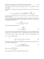
pronounced dielectric anomaly (Fig 1). For example, Fig. 1 compares the temperature
Fig. 1. Variation of the dielectric constant of a bulk ceramic and a film as a function of
temperature. [From: Shaw et al. 1999. Copyright 1999, American Institute of Physics.]
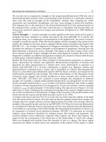
Fig. 2. Dielectric constant as a function of temperature for BST/Pt/substrate structures.
From: Taylor et al., 2002. Copyright 2002, American Institute of Physics.]
Ferroelectrics – Material Aspects
152
dependent dielectric constant of a bulk ceramic Ba
0.7
Sr
0.3
TiO
3
/BST70/30 to that of a thin film
of the same composition (Shaw et al., 1999). For the BST thin film, not only is the dielectric
constant much lower, it also does not have a sharp peak as a function of temperature. This
broad dielectric anomaly, indicative of a diffuse phase transition has been attributed to the
finer grain sizes, residual strains, composition heterogeneities inherent to synthesis (Kim et
al., 2000, Zhang et al., 2010, Mantese et al., 1995). This observed flattening of the dielectric-
temperature peak in thin film BST with respect to that of bulk ceramic BST has led many to
incorrectly conclude that BST in thin film form is temperature stable. Unfortunately, this is
not the case. When compared to bulk ceramics, thin film BST exhibits less temperature
sensitivity, (i.e., it has a smaller temperature coefficient of capacitance/TCC). However, it is
not temperature stable. Fig. 2 illustrates this temperature instability whereby Taylor and co-
workers (Taylor et al.,2002) experimentally explored the dielectric response as a function of
temperature for five BST75/25 thin films on a variety of substrates with different thermal
expansion coefficients (TECs). This work confirms that there is indeed a temperature
dependent dielectric response for thin film BST. However, BST films grown on substrates
with smaller TECs (i.e., larger tensile in-plane thermal strain) display a reduced dielectric
permittivity and a smaller (although still quite pronounced), temperature dependence of the
dielectric response. Therefore, the capacitance of any device based on such a film would be
highly temperature dependent, making its use difficult to accommodate in circuit design.
Thus, it is important to compensate for the temperature coefficient of the dielectric constant
(TCK) and the commensurate TCC. The challenge here is to accomplish this without
degrading the other device critical properties, i.e., without decreasing the tunability or
increasing the dielectric loss. This notable temperature dependence of the dielectric response
is a potential point of concern for the utilization of BST thin film in microwave devices. As
such, solutions, whether via engineering or material design must be critically reviewed and
considered.
3. Traditional temperature stability solutions
Traditional approaches to address the issue of device (phase shifter and/or tunable filter)
temperature instability have focused on employing hermetic or robust packaging, where the
package serves to protect the tunable device from the harsh environmental extremes.
Although this approach is successful, hermetic/robust packaging would add significant
cost, size, and weight to both ESA and radio systems. Other concepts to achieve temperature
stability compliance involve the use of system heat sinks and/or cooling apparatuses such
as mini-fans, temperature compensation circuits, and/or mini-ovens. Such thermal
management solutions may be utilized with ESAs or radios; however, they will add extra
weight, size, and cost to the overall system and, as such, are deemed unacceptable.
Temperature compensation can also be achieved using either a curve fit or a look-up table
approach. The curve fit methodology centers on the formulation of a temperature
dependent mathematical expression, which represents the drift of each BST tunable device.
A microprocessor utilizes this equation and the ambient temperature data (obtained from a
thermocouple mounted on the printed circuit board) to calculate the tuning voltage. The
look-up table approach, as its name implies, involves using a look-up table. In order to
obtain the relevant coefficients, the phase shifter/filter characteristics must be measured at
discrete temperatures. Then the BST bias voltage is manually adjusted to maintain the phase
shifter/filter specifications. In the worst-case scenario, one would have to obtain a set of
Performance Enhanced Complex Oxide Thin Films for Temperature Stable
Tunable Device Applications: A Materials Design and Process Science Prospective
153
points for each temperature (i.e., 23
o
C, 24
o
C etc). Typically, one would expect to have a
small subset of temperature/bias points for each bias line. The exact number of points is, of
course, dependent on the BST devices, the other phase shifter/filter components, and the
phase/filter topology. Unfortunately, both the curve fit and look-up table approaches are
quite complex as there is usually not a one-size-fits-all solution. The calibrations are also
labor and time intensive and are useful if only a limited number of ESAs, radio, and
communication devices are to be fielded.
In contrast to the above described engineering methodologies, there are also viable novel
materials science approaches. Conventional materials science methodology for reducing the
temperature dependence of an active material involve the selection of the temperature
interval of operation well above the temperature corresponding to the active material’s
permittivity maximum. Unfortunately, this approach results in reduced material tunability
and the TCC is still too high for practical military/commercial communication system
applications. More useful materials science methods for achieving material/device
temperature stability are based on utilization of artificial structures which generally involve
the synthesis of BST multilayers or compositionally graded BST structures. Such BST
heterostructures were shown to possess unique and desirable dielectric properties, i.e., a low
dependence of capacitance on temperature, high permittivities, and high tunabilities (Zhu et
al., 2003, Lu et al., 2003, Tian et al., 2003, Zhang et al., 2006). Although these experimental
and theoretical studies have produced very promising results, most of the work focused on
compositionally graded/multilayer BST films fabricated by techniques that are non-
industry standard such as pulsed laser deposition (PLD). Additionally, many of these
graded films were deposited on ceramic small-area expensive substrates, utilized “designer”
nonstandard electrodes or asymmetric electrodes, and employed high annealing
temperatures which are not compliant with conventional silicon integrated circuit (IC)
processing protocols. Specifically, the use of small-area ceramic substrates and designer
electrodes is not practical from a scale-up, manufacture, and affordability point of view and
high annealing temperatures would deteriorate the quality of the films due to the strong
diffusion between films and substrates. In the case of the metal-insulator-metal (MIM)
design, heating the film above 800 °C would damage the structure of the bottom electrode
which will degrade the dielectric loss, leakage characteristics, and tunability of the device.
Furthermore, most of the published results in the relevant literature are incomplete in that
there is a lack of systematic experimental data which determine and compare the dielectric
properties (loss, tunability, and permittivity) to those of uniform composition BST prepared
using the same fabrication technique and post-deposition anneal process protocol.
Additionally, there are relatively few investigations which evaluate the temperature
dependence of dielectric response at microwave (MW) frequencies. Nonetheless, these
studies contain important ideas and methodologies for temperature compensation and it is
important to summarize these results and populate a materials data base so that future work
can benefit from this knowledge and perhaps spawn innovative industry standard and
frequency relevant materials solutions to resolve the temperature stability dilemma.
4. Temperature stability via materials solutions
Since the concept of compositionally graded materials was originally proposed for reducing
the thermal stresses associated with dissimilar materials research in this area has been
greatly expanded from structural materials to functional materials and ultimately to thin