Applications of High Tc Superconductivity Part 9 docx
Bạn đang xem bản rút gọn của tài liệu. Xem và tải ngay bản đầy đủ của tài liệu tại đây (2.24 MB, 20 trang )
Epitaxial Oxide Heterostructures for Ultimate High-Tc Quantum Interferometers
149
flip-chip magnetometers with multilayer flux transformers having magnetic field sensitivity
below 10 fT/√Hz. Deposition and structuring are outlined for the epitaxial oxide
heterostructures; materials for substrates, epitaxial bilayer buffer, Josephson junctions and
multilayer flux transformers; the ramp-type and bicrystal Josephson junctions; operation
features, layouts, and properties of the all-oxide epitaxial multilayer high-T
c
DC SQUID
sensors including their encapsulation.
2. Deposition of epitaxial metal-oxide heterostructures
Significant technological efforts are required to produce high-quality samples of
superconducting cuprates due to their sensitivity to the compositional and structural
inhomogeneities. Accurate stoichiometry, high degree of crystallization in a single phase
and proper oxidation of the film are essential. For the deposition of epitaxial YBCO films it
is also important to have an appropriate substrate temperature and definite partial oxygen
pressure. The required purity of c-axis orientation and 123 phase of the YBCO-films is
determined by the position of the sputtering conditions in the P
O2
-T phase diagram of
YBCO. The best YBCO films are obtained along the line in the P
O2
-T phase diagram
(Hammond & Bormann, 1989) associated with initial oxygen content O
6
, which corresponds
to the absence of oxygen in the plane of the CuO chains and the CuO
2
planes of YBCO are
undoped. Three reproducible deposition methods for the fabrication of thin-film metal-
oxide heterostructures fulfilling such conditions are now mainly used: pulsed laser
deposition, reactive co-evaporation, and the high oxygen pressure magnetron sputtering
technique. These methods are briefly reviewed below with the emphasis on the high oxygen
pressure magnetron sputtering technique, which we preferentially employ for preparation
of SQUID sensors.
The reactive co-evaporation method was adopted for YBCO films by Kinder and co-workers
(Prusseit et al., 2000). By rapid cycling between deposition and oxygen reaction they
combined deposition in a high vacuum environment and oxygenation at a differentially
high oxygen pressure enclosed in the heater. The reactive co-evaporation method is
especially effective for the commercial large-scale production of epitaxial cuprate films on
large wafers or on tapes intended for high current applications such as cables for
transmission power lines, generators, and motors. The reactive co-evaporation method
provides very high material utilization efficiency, high deposition rate, possibility of
continuous deposition on km-long tapes, enabling easy switching between many elements,
and fine adjustment of the composition. One of the disadvantages of the reactive co-
evaporation method is the necessity of continuous rate control for each element of the
compounds. An atomic absorption monitor can be used for continuous measurement of the
vapour densities near to the substrates (Matias et al., 2010). The standard apparatus for
reactive co-evaporation is relatively expensive with respect to initial investments and
maintenance.
Pulsed laser deposition (PLD) is the most widely used method for the deposition of metal-
oxide heterostructures. The material that is to be deposited is vaporized from the target by a
pulsed laser beam and transported in a plasma plume to a substrate. This process can be
performed in the presence of oxygen as a background gas to oxygenate the deposited metal-
oxide films. The physical phenomena of laser-target interaction and film growth are quite
complex. The energy of the laser pulse is first converted into electronic excitation and then
into thermal, chemical and mechanical energy resulting in plasma formation, evaporation,
Applications of High-Tc Superconductivity
150
ablation, and, in some cases, even exfoliation. The ejected material is emitted from the target
in the form of atoms, molecules, electrons, ions, clusters, and even molten globules. PLD
provides a high deposition rate. A small target can be used in PLD to deposit film over
large-area wafers with appropriate scanning schemes. However, this method is also
relatively expensive, because a powerful laser is required. The films produced by PLD are
usually relatively inhomogeneous due to ablation from a spot and contamination of the
films by molten globules. There is also an angular dependence of morphology and
stoichiometry of the films prepared by PLD (Sobol, 1995) (Acquaviva et al., 2005). The
typical superconducting transition temperature T
c
of YBCO films obtained by PLD is ≈ 89 K,
which is significantly lower than T
c
≈ 93 K obtained for bulk ceramic samples of YBCO.
The technique of sputtering at high oxygen pressures allows a smart and homogeneous on-
axis in-situ deposition of high-quality metal-oxide thin films from stoichiometric targets
(Poppe et al., 1990, 1992). Conventional sputtering is used extensively in the semiconductor
industry to deposit thin films of various materials in integrated circuit processing. For the
deposition of the epitaxial metal-oxide films it is necessary to heat the substrate to
temperatures above 600
o
C and introduce oxygen into the sputtering gas atmosphere. If
conventional sputtering pressures of about 0.01 mbar are used for the on-axis deposition of
cuprate superconductors, the negatively charged oxygen ions are accelerated towards the
heated substrate by the bias potential and they thus resputter copper atoms from the
deposited film leaving copper-deficient non-stoichiometric cuprate films (see, for example,
Faley et al., 1991). With the high oxygen pressure sputtering technique, this problem is
solved by multiple scattering of the oxygen ions at background gas pressures above 1 mbar
with subsequent reduction of their kinetic energy down to thermal energies before they
reach the substrate. This results in negligible backsputtering of the copper from the
deposited films and, consequently, their good stoichiometry and electron transport
properties. Typical superconducting transition temperature of the YBCO films obtained by
this method is about 93 K and their critical current density is about 6 MA/cm
2
at 77.4 K.
The high oxygen pressure sputtering technique presupposes deposition at 0.5 to 5 mbar of a
pure oxygen (99.999%) sputtering gas atmosphere. The main feature of the sputtering
apparatus for the high oxygen pressure sputtering is the presence of a solid insulator,
typically made of MACOR, between the target holder and the ground shield. The solid
insulator prevents short circuit discharge at these relatively high sputtering pressures and a
short mean free path ∼ 0.1 mm of the accelerated electrons. If necessary, the entire range of
deposition conditions from high-energy impact to low-energy thermalized quasi-
condensation is accessible by changing the sputtering gas pressure in this apparatus. During
deposition, the substrate typically lies unrestrained on a stainless-steel heat-resistant metal
plate and is heated mainly by radiation heat transfer from a metal resistive heater. The
typical substrate temperature during deposition of the films depends on the material to be
deposited and for YBCO is ≈ 800
o
C while the heater temperature is ≈ 920
o
C.
In order to prepare multilayer heterostructures it is important that all layers should be of
sufficiently homogeneous thickness. In the case of sputtering, the trivial rule is that the size
of the target should significantly exceed the size of the substrate. Films deposited at an
oxygen pressure ≈ 3.5 mbar from 50-mm magnetron targets were only about 2.5 % thinner at
the corners of square 10-mm substrates and only 15 % thinner at the perimeter of round
wafers of diameter 30 mm compared to the film thickness in the middle of the substrates. At
the moment, the wafers up to 30 mm in diameter can be covered with heterostructures of
Epitaxial Oxide Heterostructures for Ultimate High-Tc Quantum Interferometers
151
such homogeneous thickness by the high oxygen pressure sputtering technique. Larger area
epitaxial metal-oxide heterostructures can be produced with a proper scanning apparatus or
larger magnetron targets (Faley & Poppe, 2010).
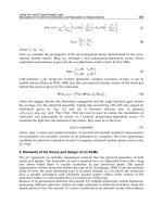
Magnetron sputtering can be used at high oxygen pressure, but it has characteristic features in
conditions of very short mean free path of electrons at pressures above 1 mbar. Large targets
require magnetic fields in order to stabilise the sputtering plasma and the optimum distance
between magnetic poles is typically in the range between 1 mm and 5 mm (Faley & Poppe,
2010). One of the magnetic poles can be replaced by a high-µ yoke made, for example, of iron
(see Figure 1a). The magnetic field of the Sm
2
Co
17
magnets in such modified target holders
additionally excites the sputtering plasma at positions away from the middle and perimeter of
the target where otherwise the plasma tends to localize. This optimized arrangement of the
Sm
2
Co
17
magnets in the magnetron target holder is mainly intended to stabilize the plasma.
Figure 1b shows an example of magnetron sputtering from a 50-mm YBCO target
demonstrating an approximately 3 mm wide ring of the most intensitive plasma region
observed at 3 mbar pressure of the pure oxygen sputtering atmosphere.
(a)
(b)
Fig. 1. High oxygen pressure magnetron sputtering: (a) sketch and (b) photograph of plasma
and target holder with a YBCO target and a MACOR insulator (Faley & Poppe, 2010).
The high oxygen pressure sputtering technique is suitable for the deposition of high-quality
epitaxial films of all metal-oxide materials required for the production of multilayer high-T
c
DC SQUID sensors. No organic material is present in the vacuum chamber of the sputtering
machine. We metallize the rear of the targets with an approximately 100 µm thick silver
layer, which is partially diffused into the targets at 850
o
C to a depth of about 30 µm, and we
bond them to the Cu holder by soldering with AgSn solder. The diffusion coefficient of Ag
into bulk YBCO ceramic samples is D
Ag
≈ 4.5 x 10
-9
cm
2
/s at 850
o
C (Dogan, 2005).
The base pressure in the deposition chamber for YBCO was about 2⋅10
−7
mbar while
sputtering of YBCO was performed at ≈ 3.5 mbar pressure of pure (99.999%) oxygen. The
DC sputtering technique is usually used for deposition from sufficiently conducting targets,
while in the case of more insulating targets deposition is carried out by the RF sputtering
technique. The typical deposition rate obtained with the DC sputtering technique was about
90 nm/hour while in the case of RF sputtering it was about 20 nm/hour.
The surface morphology of the films is crucial for the preparation of multilayer structures.
Depending on the deposited material, the epitaxial growth of metal-oxide films proceeds in
the following three modes: Frank-Van der Merwe growth (layer-by-layer); Volmer-Weber
growth (3-D nucleation); or Stranski-Krastanov growth (mixed mode). The YBCO films
grow in the Stranski-Krastanov growth mode: initial layer-by-layer growth changes to spiral
Applications of High-Tc Superconductivity
152
growth for films thicker than about 20 nm (Dam et al., 2002). The growth spirals on YBCO
films have an average height of about 30 nm and their in-plane size strongly depends on the
deposition temperature. The optimum substrate temperature is ≈ 100
o
C higher during high
oxygen pressure sputtering compared to that in the case of the PLD deposition method. This
explains the width of the growth spirals of up to ≈ 900 nm observed on the surface of the
YBCO films deposited by the high oxygen pressure sputtering technique (Faley et al., 2006b)
compared to the ≈ 200 nm wide growth spirals on the YBCO films deposited by PLD (Dam
et al., 1996). The morphology of the YBCO films is one of the factors contributing to the
spread of the parameters of high-T
c
bicrystal Josephson junctions with misorientation angles
below 24 deg and thicknesses < 60 nm as well as to the quality of the insulation layers.
3. Materials used for the high-T
c
heterostructures
For the most efficient coupling of magnetic fields to a SQUID loop, a multilayer flux
transformer with at least two high-T
c
superconducting epitaxial, usually, YBCO layers
separated by an insulator layer is required. The technological and structural compatibility of
the materials involved is an important precondition for the heteroepitaxial growth of the
multilayer structures of the high-T
c
SQUIDs and flux transformers. The oxygenation of the
bottom YBCO films is only possible if there is sufficient mobility of oxygen ions in the
insulating layer. An epitaxial buffering of substrates intended for the deposition of the high-
T
c
heterostructures can improve further device properties.
The non-superconducting material most compatible technologically with YBCO is
PrBa
2
Cu
3
O
7-x
(PBCO), which has thermally activated hopping-type electrical conductivity
(Fisher et al., 1994) and the perovskite-derived crystal structure is isomorphic to that of
YBCO. The lattice constants of PBCO are a = 3.873 Å, b = 3.915 Å, c = 11.67 Å, which are
very close to those of YBCO: a = 3.823 Å, b = 3.88 Å, c = 11.68 Å. Due to the similarity of the
crystal structures of PBCO and YBCO a very low charge carrier scattering and negligible
contact resistance were observed for the interfaces between the films of PBCO and YBCO
(Faley et al., 1993). The PBCO films were successfully used for buffer layers, tunnel barriers,
and for non-superconducting insulators in the SQUID-related heterostructures with YBCO.
It was observed that the electrical insulation in the YBCO-PBCO-YBCO heterostructures
could be significantly improved by passivation of the bottom YBCO layer by a brief
application of ion beam etching (Faley et al., 1997a). The reason for the increased contact
resistance was a cation-disordered cubic phase of YBCO that appeared after the
amorphization of the surface layer of YBCO by the ion bombardment followed by the
recrystallization of this surface layer at high temperatures during the deposition of the top
film (Jia et al., 1995). A further improvement in insulator resistance was achieved by
implementation of a PBCO-STO electrically insulating heterostructure (Faley et al., 2010).
The 50 nm PBCO film served as a buffer layer followed by the 300-nm thick STO insulator
film deposited in-situ. The PBCO film improved epitaxial growth of the STO film over the
substrate and the bottom YBCO film as well as the morphology and resistance of the
insulator layer in the direction normal to the substrate surface. The resistance of the PBCO
film along the substrate surface contributed to dumping of microwave resonances in the
input coil of the multilayer flux transformer.
The best structural and superconducting parameters of YBCO films are typically obtained
on STO substrates. Epitaxial STO films have also provided an excellent template for the
epitaxial growth of the top YBCO film of the top superconducting layer in the thin film
Epitaxial Oxide Heterostructures for Ultimate High-Tc Quantum Interferometers
153
superconducting flux transformers. Figure 2 shows the high-resolution transmission
electron microscopy (HRTEM) image of the interface region between epitaxial STO and
YBCO films produced by the high oxygen pressure sputtering technique and demonstrates
the high-quality microstructure of these films.
Fig. 2. Cross-sectional HRTEM image of the interface between YBCO and STO films
obtained in the [110] direction (Faley et al., 2008).
Coverage of the bottom YBCO layer by the epitaxial STO films in the YBCO-STO-YBCO
heterostructures does not degrade the superconducting properties of the bottom YBCO film.
STO enables sufficient diffusivity of oxygen ions required for the full oxygenation of the
YBCO films at, typically, about 500
o
C. The diffusion coefficient of oxygen ions in single
crystal STO is known to be D
O
= 5.2⋅10
-6
⋅exp(-11349/T) cm
2
/sec in the temperature range
between 850
o
C and 1500
o
C (Paladino, 1965). Assuming this dependence can be extended to
lower temperatures and that the diffusivity of oxygen in STO films is similar to that in single
crystal STO samples, the estimated time required to oxygenate a YBCO film covered by a 0.5
µm thick STO film is about 1.5 hour at 500
o
C substrate temperature. Indeed, our empirically
obtained optimum oxygenation time for the YBCO-STO-YBCO heterostructures used in the
high-T
c
superconducting flux transformers is about 2 hours. The input coil included a 200
nm bottom YBCO film, which was covered by the approximately 400 nm PBCO-STO
insulator heterostructure and 600 –1000 nm top YBCO film. A 100 nm thick silver film
served to protect the top YBCO layer during structuring with AZ-photoresist.
Another useful substrate material for SQUIDs is MgO, which has a thermal expansion
coefficient similar to that of YBCO (∼ 14 x 10
-6
) (see Table 1). The difference in the thermal
expansion coefficients of the oxide materials such as STO, LaAlO
3
(LAO), NdGaO
3
(NGO),
Al
2
O
3
, and YSZ often used for the substrates and films leads to a very strong tensile strain in
the YBCO films degrading their superconducting properties and can even crack the films
when their thickness exceeds some critical value. Much thicker multilayer high-T
c
thin film
structures with smaller capacitance can be produced on MgO substrates. An additional
advantage of MgO is that it has a relatively low dielectric constant ε ≈ 9 and low losses tan δ
≈ 3.3⋅10
−7
. It is one of the traditional materials used in microwave electronics. The low
dielectric constant of MgO leads to a smaller parasitic capacitance through the substrate
across the inductance of the DC SQUID loop compared to the DC SQUIDs on STO
substrates. This leads to smaller voltage swings, but also lower white noise of high-T
c
DC
SQUIDs on MgO substrates compared to those on STO substrates (Enpuku et al, 1996).
Applications of High-Tc Superconductivity
154
Linear thermal
expansion
(in 10
-6
/K
)
Crystal structure
Lattice
constant (Å)
Dielectric
constant
MgO
∼ 14
cubic, rock-salt 4.21
∼ 10
BaZrO
3
∼ 7
cubic, perovskite 4.19
∼ 20
SrTiO
3
∼ 11
cubic, perovskite 3.91
∼ 270
NdGaO
3
∼ 6
orthorhombic, perovskite 3.85
∼ 20
LaAlO
3
∼ 9
rhombohedral, perovskite 3.82
∼ 24
YBa
2
Cu
3
O
7-x
∼ 13.5
orthorhombic, perovskite 3.85
∼ 5
Table 1. Selected properties of materials for substrates and buffer layers used for deposition
of YBCO.
Unbuffered MgO substrates demonstrate degradation of the hygroscopic surface in air and
have a large lattice mismatch of ≈ 9 % with YBCO and a crystal structure that differs from
YBCO. These features usually lead to appearance of in-plane 45
o
misoriented grains in the
YBCO films deposited on MgO substrates. The average critical current density of the YBCO
films is in this case usually significantly suppressed at the boundaries between the grains
and the magnetic noise of the YBCO films is drastically increased. Single-layer buffers such
as BaZrO
3
(BZO) or STO films only slightly improved this situation. At least two buffer
layers are required to deposit low-noise YBCO films on MgO: the first one should provide
the epitaxial growth of films with perovskite structure on the rock-salt structure of MgO,
while the second buffer layer should match the lattice constants. STO and BZO films are
technologically compatible with YBCO and have the required structural properties.
An epitaxial perovskite double-layer STO/BZO buffer on MgO substrates has been
developed for the deposition of low-noise and crack-free YBCO films (Faley et al., 2006a).
This buffer also protects the hygroscopic surface of the MgO substrates against degradation
in air and/or during the lithographic procedures. Figure 3 shows a cross-sectional HRTEM
image of a BZO-STO-YBCO heterostructure deposited on a MgO (100) substrate.
Fig. 3. Cross-sectional HRTEM image of a BZO-STO-YBCO heterostructure deposited on an
MgO (100) substrate (Faley et al., 2006a).
It was observed that the antiphase boundaries (APB), which appeared at the BZO/MgO
interface and spread through the BZO layer, usually disappeared at the STO/BZO interface
(Mi et al., 2006). The STO layer initially grows with the lattice constant expanded to the
Epitaxial Oxide Heterostructures for Ultimate High-Tc Quantum Interferometers
155
lattice constant of BZO ≈ 4.19 Å. However, just a after few unit cells from the STO/BZO
interface the lattice constant of STO already relaxed to its bulk value ≈ 3.91 Å (see Figure 4).
Fig. 4. Cross-sectional HRTEM image of an interface region for BZO and STO films
deposited on a MgO (100) substrate (Mi et al., 2007).
Thus, at the YBCO/STO interface the lattice constant and microstructural quality of the STO
layer is similar to that of the single-crystal STO substrate, but the overall thermal expansion
coefficient is still determined by the 1 mm thick MgO substrate. The YBCO films deposited by
high oxygen pressure sputtering technique naturally contain lattice-coherent non-
superconducting Y
2
O
3
nanoparticles, which are nearly spherical with a diameter of ~20 nm
and are homogeneously distributed with a separation of ~30 nm (Faley et al., 2006b) and
provide a strong 3D pinning of the Abrikosov vortices leading to a high critical current density
J
c
and a low magnetic noise in the films (Kim et al., 2007). Even 5-µm-thick YBCO films on the
buffered MgO substrates do not display cracks and demonstrate a critical current density ≈ 3.5
MA/cm
2
at 77 K (Faley et al., 2008). The 1 cm wide films have an estimated total critical
current of ≈ 1.7 kA at 77 K, which is about 17 times greater than the critical current of the
present day 2
nd
-generation high-T
c
superconducting tapes of similar width. Such high and
homogeneous critical current densities of the high-T
c
superconducting films are beneficial for
production of the low-noise SQUID sensors, for high-Q microwave resonators and filters in
communication technologies as well as for high-T
c
superconducting tapes intended for the
generation and transport of electrical power. The YBCO films deposited on the buffered MgO
substrates demonstrated conductivity proportional to the film thickness for up to about 5 µm
thick films (Faley et al., 2006a). The specific conductivity of YBCO films on other substrates
such as STO, LAO, NGO, Al
2
O
3
, and YSZ was saturated or even dropped when the film
thickness exceeded the critical values and cracks appeared in the YBCO films.
4. Patterning techniques for epitaxial metal-oxide multilayers
In the case of the epitaxial metal-oxide multilayers for high-T
c
SQUIDs it is essential to avoid
grain boundaries in the superconducting films because the thermally-activated hopping of
flux vortices and fluctuations of superconducting current at the grain boundaries often act
Applications of High-Tc Superconductivity
156
as sources of flicker noise in the SQUIDs. Patterning of bottom layers should leave
chemically clean and bevelled edges of the structures for the homogeneous epitaxial growth
of top superconducting layers over the edges. Such structuring can be achieved by non-
aqueous chemical etching as well as by the ion beam etching methods briefly described
below.
Chemical etching in a Br-ethanol solution in combination with a deep-UV photolithography
of PMMA photoresist was used for the patterning of YBCO-PBCO heterostructures to
prepare the high-T
c
Josephson junctions, crossovers, and interconnects (Faley et al., 1993). It
was observed that the chemical etching of c-axis-oriented YBCO and PBCO films through a
mask of PMMA photoresist is very anisotropic: it is much faster along the ab-planes than in
the c-direction of the films. This causes abnormally large undercutting, which results in very
gently sloping edges of the structures (see Figures 5 and 6). The angle α of slope of the edge
is about 3 degree with respect to the substrate plane. This angle can be increased by
extending the etching time or in combination with ion beam etching.
Fig. 5. Optical image of a 500-nm thick YBCO-PBCO bilayer etched through a mask of
PMMA photoresist by the Br-ethanol solution. The upper part of the picture shows the film,
while the lower part shows the STO substrate. The bright horizontal stripe in the middle of
the picture is the chemically prepared edge.
Fig. 6. A low-magnification TEM picture. This picture gives an overview of a cross-section of
a YBCO-PBCO-YBCO edge structure, containing the bottom YBCO film, the insulating
PBCO layer, the PBCO barrier and the top YBCO film (Faley et al., 1993).
The main advantage of the non-aqueous chemical etching in Br-ethanol solution is that the
edge area is not contaminated by substrate material and shows negligible structural damage at
the surface layer. Moreover, this solution does not change the local stoichiometry at the surface
and, in contrast to the ion beam etching, it does not even affect the oxidation state of the
copper (Vasquez et al., 1989). Bromides YBr, BaBr or CuBr are soluble in ethanol and,
therefore, the surface of the edge appears to be very clean after etching followed by rinsing in
ethanol. The chemical etching in Br-ethanol solution was used for the preparation of the ramp-
type high-T
c
Josephson junctions and the bottom layers, YBCO and PBCO, in the multilayer
flux transformers with PBCO insulation layer (Faley et al., 2001). If an STO film was used for
the insulation between the YBCO films, the bottom YBCO layer can also be etched by the
chemical etching. The lower superconducting layer used for the return lead of the input coil
Epitaxial Oxide Heterostructures for Ultimate High-Tc Quantum Interferometers
157
and the pick-up loop does not require high precision in structuring and it was patterned with
deep-UV lithography using a PMMA-photoresist and Br-ethanol chemical etching.
Ion beam etching enables sub-micrometer precision in structuring the films through masks
of AZ-type (mainly AZ5214E and AZ MIR701) photoresists. Upper superconducting layers
in the ramp junctions and flux transformers contain µm-size structures and required
conventional patterning with AZ photoresist and ion beam etching. Ion beam etching can be
also used for structuring the bottom YBCO layer and insulation layer under condition of
sufficiently low-angle edges of the photoresist mask. Proper cleaning with microstructural
restoration of the edge surface should follow the etching. Bevelling of the AZ-photoresist
edges down to an angle below 20 degrees relative to the substrate plane can be realized by
backing-out of the photoresist at 130
o
C (David et al., 1994).
Cleaning and restoration of the edge surface after etching is more difficult in the case of the
ion beam etching as compared to Br-ethanol chemical etching. Rinsing and mechanical
polishing in acetone and methanol followed by annealing in the presence of oxygen plasma
can remove the photoresist, including carbonized parts of photoresist near the edges, as well
as the amorphous materials redeposited on the edges of the photoresist structures during
ion beam etching. Annealing in the presence of oxygen plasma also leads to recrystallization
of the surface of edges of the etched film, which partially recovers its microstructural and
electron transport properties. A high quality of the crossovers and vias in the multilayer
multiturn coil of the flux transformer is essential to obtain high values of the induced
superconducting current. Due to the damage-free interfaces and gently sloping edges
produced by Br-ethanol etching we achieved critical currents for the flux transformers of
about 100 mA at 77 K. The observed 60 µT peak-to-peak dynamic range of the
magnetometer having 8-mm pick-up loop (L
pu
≈ 20 nH) is limited mainly by this critical
current of the flux transformer.
We use both patterning techniques – non-aqueous Br-ethanol chemical etching and ion
beam etching – for the preparation of sensitive high-T
c
multilayer DC SQUID sensors with
reduced low frequency noise, which are described in the following sections.
5. Multilayer high-T
c
DC SQUID magnetometers
In this section, the review of multilayer high-T
c
DC SQUID flip-chip magnetometers will
include a short introduction to the principle of operation of DC SQUIDs, a description of
their noise properties and basic components: high-T
c
Josephson junctions, superconducting
multilayer flux transformers with multiturn input coil, and capsulation. The reproducibility
of the high-T
c
Josephson junctions is especially important in the case of implementation of
the high-T
c
DC SQUID arrays. The vacuum-tight encapsulation of the sensors is a
prerequisite for their long-term stability, easier handling, and for the reduction of low-
frequency noise by removing the magnetic flux trapped in the superconducting films.
5.1 DC SQUIDs – principle of operation
SQUIDs consist of a loop of superconductor interrupted by one or two Josephson junctions.
The operation of SQUIDs is based on the dependence of phase shift Δϕ of quantum wave-
functions
Ψ
of Cooper pairs on magnetic flux Φ passing through the SQUID loop. This
dependence is caused by the fundamental dependence of the canonical momentum
p
mv
q
A=+
and, consequently, de Broglie wavelength /h
p
λ
=
and wave vector
/kp=
Applications of High-Tc Superconductivity
158
of charged particles on magnetic vector potential
A
. The superconducting wave function
exp( )i
ϕ
Ψ= Ψ has the spatial variation of the phase
(,)rt
ϕϕ
=
due to the presence of the
vector potential
A
of the magnetic field threading through the SQUID loop. The phase
difference
12
δϕ
−
of the wave function at positions x1 and x2 is
22 2
12
0
11 1
2
xx x
xx x
q
kdl Adl Adl
π
δφ
−
== =
Φ
, where
0
//2hqh eΦ= = ≈ 2.07 10
-15
T⋅m
2
is the
magnetic flux quantum.
The superconducting wave function
exp( )i
ϕ
Ψ= Ψ is continuous in the superconductor up
to the Josephson junctions. The requirement that the superconducting wave function Ψ have
a single value everywhere is an important boundary condition for SQUID operation. At the
Josephson junctions, the jump of phase Δϕ of the wave functions in individual
superconducting electrodes is detected according to the Josephson current-phase
relationship I(ϕ) = I
c
sin(Δϕ). This quantum interference leads to a periodic dependence of
the output voltage of SQUIDs on applied magnetic flux Φ threading through the SQUID
loop thus enabling the SQUIDs to convert tiny changes in magnetic flux Φ into measurable
voltage signals.
Fig. 7. Schematic representation of the DC SQUID loop with values of the superconducting
wave-function Ψ, critical currents I
S1
and I
S2
of the Josephson junctions J1 and J2,
respectively, and the magnetic flux Φ penetrating through the SQUID loop.
Direct-current SQUIDs (DC SQUIDs) consist of a loop of two superconducting electrodes E1
and E2 connected together by two Josephson junctions denoted as J1 and J2 in Figure 7. DC
SQUIDs are sensitive flux-to-voltage transducers: when a flux Φ of the magnetic field
penetrates the DC SQUID loop, the spatial variations of the phase of the wave function Ψ of
Cooper pairs in superconducting electrodes appears. These lead to the phase shifts Δϕ
2
and
Δϕ
2
between the wave functions in the superconducting electrodes at the Josephson
junctions and, consequently, to a voltage signal on the DC SQUIDs.
Epitaxial Oxide Heterostructures for Ultimate High-Tc Quantum Interferometers
159
The operation of DC SQUIDs can be explained most clearly in the first approximation of the
zero-voltage state, for a small and symmetric DC SQUID loop. In the zero voltage state of
the Josephson junctions the phase
ϕ
of the wave function of Cooper pairs does not depend
on time. Without magnetic flux threading of the DC SQUID loop (
Φ
= 0) the maximal
superconducting current I = I
S1
+I
S2
= I
C1
+I
C2
is achieved at the phase difference
Δϕ
1
=
Δϕ
2
=
π
/2+ 2
π
n between the phases of the wave functions in electrodes at points E1 and E2 because
only in this case I
S1
=I
C1
and I
S2
=I
C2
(see Figure 7).
Magnetic flux AdlΦ=
≠ 0 changes the phase shifts
111 1
2
2
n
π
φφ
δ
φ
δ
φ
π
∗
Δ=Δ+ =+ +
and
222 2
2
2
n
π
φφ
δ
φ
δ
φ
π
∗
Δ=Δ+ =+ +
due to the non-zero integral of the vector potential A
along
the superconducting parts of the SQUID loop. The phase shifts
Δϕ
1
and
Δϕ
2
are
11
1
00 0
21
22
JJ
EE
Adl Adl
πππ
δϕ
Φ
=−=
ΦΦΦ
and
22
2
00 0
21
22
JJ
EE
Adl Adl
πππ
δϕ
Φ
=−=−
ΦΦ Φ
, in the case of
geometrically symmetric SQUID loops like the one shown in Figure 7. Thus, in the present
of a magnetic field, the phase differences at the Josephson junctions are:
1
0
2
2
n
ππ
ϕπ
∗
Φ
Δ=+ +
Φ
and
2
0
2
2
n
ππ
ϕπ
∗
Φ
Δ=+ −
Φ
. The total maximal superconducting current through the SQUID is
thus
12 1 1 2 2
sin( ) sin( )
SSC C
II I I I
ϕ
ϕ
∗∗
=+= Δ+ Δ. In the case of Josephson junctions with similar
critical currents I
C1
= I
C2
= I
C
the total current through the DC SQUID is:
12
00
sin( ) sin( ) 2 sin( 2 )cos 2 cos
2
CC C
II I n I
ππ π
ϕϕ π
∗∗
ΦΦ
=Δ+Δ= + =
ΦΦ
(1)
at Φ < Φ
0
/2. A further increase of flux changes the phase difference between the wave
functions at points E1 and E2 from π/2 to -π/2 (in both cases I=0 at Φ = Φ
0
/2) so that the
maximal superconducting current through such DC SQUID I
max
is always positive and is a
periodic function of Φ with period Φ
0
:
max
0
2cos
C
II
π
Φ
=
Φ
(2)
In the dissipative regime (at bias currents I
B
> 2I
C
) there are periodic series of pulses
(Josephson oscillations) of voltage U(Φ,t) across the DC SQUID. Averaging of U(Φ,t) over
the period τ of the Josephson oscillations results in the dc voltage V across the DC SQUID
(Tinkham, 1996):
()
2
0
0
2
1
,1cos
2
NB C
B
RI I
VUtdt
I
τ
π
τ
Φ
=Φ≈ −
Φ
(3)
where R
N
is the resistance of the individual Josephson junction in the DC SQUID. The dc
voltage V across the DC SQUID is a periodic function of the magnetic flux Φ through the
SQUID loop.
Applications of High-Tc Superconductivity
160
5.2 Josephson junctions for the high-T
c
DC SQUIDs
The Josephson junctions in SQUIDs transform the phase changes of the superconducting
wave functions into measurable voltages owing to the Josephson current-phase relationship
I(ϕ) = I
c
sin(Δϕ). A Josephson junction is made by sandwiching a thin layer of a non-
superconducting material between two layers of superconducting material(s). With a
sufficiently thin barrier, the phase of the electron wave-function in one superconductor
maintains a fixed relationship with the phase of the wave-function in another
superconductor. In this way, the superconductors preserve their long-range order across the
insulating barrier in the Josephson junctions.
Mainly ramp-type, step edge and bicrystal grain boundary high-T
c
Josephson junctions are
used for high-T
c
SQUIDs. The best reproducibility of the junction parameters was obtained
for the ramp-type and bicrystal grain boundary high-T
c
Josephson junctions shown
schematically in Figure 8.
(a)
(b)
Fig. 8. Schematics of the ramp-type (a) and bicrystal (b) high-T
c
Josephson junctions.
Ramp-type Josephson junctions contain two superconducting layers separated by a barrier
layer deposited on the edge of the bottom superconducting layer (see the Figure 8a).
Electron transport on the top of the bottom layer is prevented by a thick insulation layer.
The barrier material and thickness can be chosen for optimum performance in particular
applications. The ramp junctions on the chemically etched edges with PBCO films as the
barrier and insulation layers have proven parameters that are sufficient for many
applications of DC SQUIDs (Faley et al., 1995 and 1997b). The ramp junctions have the
advantage that relatively cheap single crystal substrates can be used. On the other hand,
compared to the bicrystal junctions, production of SQUIDs with ramp junctions is more
complicated and for a similar critical current I
c
their normal state resistance, R
N
, is about 3
times smaller leading to smaller voltage swings of the DC SQUID. The easier production of
junctions on bicrystal substrates and the smaller contribution of the noise of SQUID control
electronics to the total noise of the measurement system have led to the preferred utilization
of bicrystal junctions in high-T
c
DC SQUIDs.
The bicrystal junctions optimized for operation in high-T
c
DC SQUIDs typically have a
width ≈ 1 µm, resistance R
N
≈ 6 ohm, and a critical current I
c
≈ 25 µA at 77 K. Dependence of
the critical current density of bicrystal Josephson junctions J
c
on the misorientation angle Θ
can be approximated at 77 K by the following expression (Ivanov et al., 1991):
Epitaxial Oxide Heterostructures for Ultimate High-Tc Quantum Interferometers
161
()
()
26
de
g
.
/4.1610exp( )
4.2
c
JAcm
θ
≅⋅⋅−
(4)
As was revealed by TEM studies, the effective thickness L of the distorted layer at the
bicrystal grain boundary increases approximately linearly with Θ and it was suggested that
the exponential decrease of J
c
(Θ) is associated with this increase of the distorted layer.
Typical critical current density J
c
≈ 10 kА/сm
2
in the bicrystal high-T
c
Josephson junctions
used for DC SQUIDs operating at 77 K.
For high-T
c
bicrystal Josephson junctions the resistance R
N
is determined by both direct
tunnelling and the resonance tunnelling components of charge carrier transport through the
grain boundary (Halbritter, 1985). The total conductance of the junction with the cross-section
area σ = 0.2 µm
2
can be approximated by the following expression (Minotani et al., 1998):
1/2
1/ 2150 11
Ncc
GR II=≅+
(5)
where the critical current I
c
=J
c
σ is in amperes at 77 K while the resistance R
N
is in ohms for
the bicrystal junctions width ≈ 2 µm and the YBCO film thickness ≈ 100 nm. The second
term in (5) representing the resonance tunnelling prevails at the bicrystal misorientation
angles above about 24 degree. The I
c
R
N
product is ≈ 200 µV at the bicrystal in-plane
misorientation angle 24 degree and temperature 77 K:
1/2
1/(2150 11 )
cN c
IR I
−
≅+
(6)
The I
c
R
N
product decreases with increase of the misorientation angle and corresponding
decrease of the critical current density of the junction. This decrease is especially strong for
misorientation angles above 24 degree, where it was found that I
c
R
N
∝√J
c
(Gross et al., 1997).
The critical current density J
c
of symmetric 24 degree bicrystal Josephson junctions increases
nearly linearly with the temperature dependence J
c
(T) ≈ 10
4
[4.1+6.4(60-T)/40] A/cm
2
in the
range of operating temperatures T = (10 - 80) K. Noise parameter Γ = 2πk
B
T/I
c
Φ
0
= I
th
/I
c
for
a particular junction depends strongly on the temperature: for the junctions having I
c
≈
20 µA at 77 K the noise parameter Γ is ≈ 0.16 at 77 K, Γ ≈ 0.05 at 63 K, and Γ ≈ 0.005 at 20 K.
The Stewart-McCumber parameter of the Josephson junctions
2
0
2/
CCN
IRC
βπ
=Φ increases
with reduced temperature and increased critical current from
C
β
≈ 0.12 at 77 K to ≈ 0.34 at
63 K and ≈ 1 at 20 K. Below ≈ 20 K the Josephson junctions become hysteretic. The
capacitance C of the bicrystal grain boundary Josephson junction C = σεε
0
/t ≈ 25 fF for the
junction width w = 2 µm and YBCO film thickness d = 100 nm (the junction area σ = w⋅d ≈ 2
10
-9
cm
2
). The grain boundary of the YBCO bicrystal junctions behaves as if it were mostly
dielectric with an average barrier thickness t ≈ 2 nm (Winkler et al., 1994) and dielectric
constant ε ≈ 28 for the grain boundary region in YBCO (Navacerrada, 2008).
Both the noise parameter Γ and the Stewart-McCumber parameter
C
β
contribute to the
voltage noise of the Josephson junctions (Voss, 1981) and, consequently, to the magnetic
field resolution of the DC SQUID magnetometers. Reduction of temperature from the
standard operating temperature of high-T
c
SQUIDs 77 K to, for example, the triple point of
nitrogen 63 K leads to an increase of I
c
and a reduction of Γ, but also to increase of voltage
noise due to the increase of
C
β
. An external resistive shunting of the junctions helps to
reduce
C
β
and, consequently, voltage noise at lower temperatures and to avoid transition
of the Josephson junctions to the hysteretic mode.
Applications of High-Tc Superconductivity
162
5.3 Performance and noise of high-T
c
DC SQUIDs
The average dc voltage V across the DC SQUID is a periodic function of magnetic flux Φ
with the period equal to the magnetic flux quantum Φ
0
. At final temperatures T > 0, the I(V)
characteristics of Josephson junctions are rounded by thermal noise and the bias current I
B
corresponding to the maximal voltage response
∂V/∂Φ is smaller than the total critical
current of symmetric DC SQUID 2I
c
(Drung et al., 1996):
0
0
11
2
B
BB
c
B
I
IkT
I
kT
Φ
≈+ ++
Φ
(7)
The optimum bias current I
B
of high-T
c
DC SQUIDs is (40 ± 30) µA at 77 K. At bias currents
I
B
> 70 µA the voltage response ∂V/∂Φ is reduced due to circulation of shielding currents
in the DC SQUID loop at the typical high-T
c
DC SQUID inductances L
S
of about 100 pH. The
inductance L
S
of the DC SQUID loop reduces the voltage response to the magnetic flux in
two ways: first, the induced currents shield significantly the magnetic flux through the
SQUID loop at L
S
> Φ
0
/2I
c
and, second, due to the rounding of the current-voltage
characteristics by thermal flux noise δΦ = √k
B
TL
S
. At bias currents I
B
< 10 µA the critical
currents I
c
< 5 µA become comparable to the thermal current I
th
= 2πk
B
T/Ф
0
~ 3.3 µA
leading to reduction of the voltage response
∂V/∂Φ of the SQUIDs. Taking into account
the inductance of the DC SQUID loop L
S
and operating temperature T, the maximum
voltage response
∂V/∂Φ of DC SQUID under optimum operation conditions Φ ≈
(2n+1)Φ
0
/4, where n = 0, ±1…, is determined by the expression (Enpuku et al., 1995):
2
2
0
0
0
4
exp( 3.5 )
2
1
cN B S
cS
IR kTL
V
IL
π
∂
≈⋅ ⋅ −
∂Φ Φ
Φ
+
Φ
(8)
Taking into account the voltage noise of the Josephson junctions, the magnetic flux noise of
the high-Tc DC SQUID can be estimated according to the following expression:
2
222
22
2
2
1
81
42
ScS
D
VB
NN N
LIL
VRV V
SS kT
RR I R
−−
Φ
∂∂∂
=≈+ + ∝
∂Φ ∂Φ ∂Φ
(9)
for L
S
> 40 pH and neglecting the noise of the preamplifier of the control electronics. The
dynamic resistance of the symmetric DC SQUIDs is R
D
= ∂V/∂I ≈ R
N
/√2 (Ryhänen et al.,
1989), where R
N
is the normal state resistance of a single Josephson junction in the DC
SQUID. At inductances L
S
< 40 pH the R
D
term in (9) prevails over the second term and the
flux noise of the DC SQUID is saturated.
The white flux noise of the SQUIDs is determined mainly by the thermal fluctuations in the
Josephson junctions, by the maximum voltage response to the magnetic flux
∂V/∂Φ and
by the noise of the preamplifier of the control electronics S
Ve
:
22
222
12
//
24
NS
B
VVe
N
RL
VkT V V
SS S
R
Φ
∂∂∂
=≈ ++
∂Φ ∂Φ ∂Φ
(10)
at the bias current I
B
≈ 2I
c
.
The white flux noise of DC SQUIDs was calculated according to the expression (11) with S
Ve
≈ 0.2 nV. The obtained value of the flux noise ≈ 3 µΦ
0
/√Hz for a 40-pH DC SQUID fits well
Epitaxial Oxide Heterostructures for Ultimate High-Tc Quantum Interferometers
163
with the measured value ≈ 4 µΦ
0
/√Hz. The inductances of the SQUID loop and other multi-
layered superconducting circuits were estimated with the help of software package 3D-
MLSI (Khapaev et al., 2003).
The high dynamic range of the DC SQUID measurement system is achieved by linearization
of the DC SQUID output signal with the help of DC SQUID control electronics, which
compensated most of the applied magnetic flux by a flux-lock-loop circuit. Operation of the
DC SQUID control electronics in bias reversal mode led to an approximately 3-fold
reduction in the intrinsic low-frequency noise originating from fluctuations of critical
currents of the Josephson junctions in the high-T
c
DC SQUIDs. As was verified, the high-T
c
DC SQUID sensors are compatible with the commercially available bias-reversal DC SQUID
control electronics from Tristan Technologies Inc., Cryoton Ltd., Supracon AG, Magnicon
GmbH, and STL Systemtechnik Ludwig GmbH. The hybrid digital electronics provide
especially high slew rate up to 5 MΦ
0
/sec, dynamic range up to about 130 dB and frequency
range up to about 10 MHz for the measurement system with multilayer high-T
c
DC SQUIDs
operating at 77 K (Ludwig et al., 2001). The above-mentioned DC SQUID electronics have
the noise of preamplifier S
Ve
≈ (0.2 nV)
2
/Hz. For applications in the frequency range up to
about 20 kHz, the modulation electronics with a raised transformer between the SQUID and
the DC SQUID control electronics has the advantage of a convenient and stable operation of
the measurement system.
5.4 High-T
c
DC SQUID magnetometers with inductively coupled multiturn input coil
High sensitivity of SQUIDs magnetic fields can be provided by different superconducting
flux transformers, which concentrate or convert the weak magnetic fields to be measured
into the significant magnetic flux threading through the SQUID loop. The concentrating
types of superconducting flux transformers such as large SQUID washer, additional single-
layer thin-film concentrator or bulk flux concentrator, or direct coupled superconducting
flux antenna, have relatively inefficient flux transfer and a low effective area A
eff
caused by
the large difference between the inductance of the SQUID loop L
S
∼ 80 pH and the
inductance of the concentrator pick-up loop L
pu
∼ 40 nH.
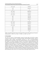
Figure 9 shows the flux sensitivity S(nT/Φ
0
) ≈ 2.068/A
eff
(mm
2
) of the flip-chip
magnetometers with multiturn input coil in comparison to one of the direct-coupled
magnetometers. The effective area A
eff
of a direct-coupled magnetometers is proportional to
A
pu
L
S
/L
pu
∝ a, where a is the size of the pickup coil; A
pu
∝ a
2
is its area; and L
pu
∝ a is its
inductance. For the single-layer directly coupled magnetometers with a pickup loop 20 mm
x 20 mm, inductance of the SQUID loop ≈ 50 pH, and flux sensitivity S ≈ 4.6 nT/Φ
0
, the best
magnetic field resolution ≈ 24 fT/√Hz at 1 Hz and ≈ 14 fT/√Hz at 1 kHz was obtained at
77 K (Cantor et al., 1995).
Much better coupling can be achieved with a multiturn input coil, which is connected in
series to the pick-up coil and inductively coupled to the SQUID loop. The effective area A
eff
∝ A
pu
⋅√(L
S
/L
pu
) ∝ a
3/2
and exceeds the effective area of a direct-coupled magnetometer in
about 3 times for 8 mm pick up coils and in about 10 times for 20 mm pick-up coils.
Field resolution of the inductively coupled magnetometers with multiturn input coil is:
1/2
1
pu i
S
N
N
pu i S
LL
L
BS
kR
kA L L
Φ
+
=∝ (11)
Applications of High-Tc Superconductivity
164
Fig. 9. Flux sensitivity S(nT/Φ
0
) vs pick-up loop size a(mm) for direct coupled
magnetometers (
■, S
dc
) and for the inductively coupled magnetometers with multiturn input
coil (
■, S
ind
) (Faley et al., 2001).
An important prerequisite for the application of high-T
c
SQUIDs for MEG is a magnetic field
resolution below 10 fT/√Hz at 77 K. Such magnetic field sensitivities have only been
achieved with high-T
c
direct current superconducting quantum interferometers (DC
SQUIDs) inductively coupled to epitaxial multilayer thin-film flux transformers with a
multilayer multiturn input coil. The Berkley group (Dantsker et al., 1995) has demonstrated
flux sensitivity S ≈ 1.7 nT/Φ
0
magnetic field resolution ≈ 27 fT/√Hz at 1 Hz and ≈ 8.5
fT/√Hz at 1 kHz using a flip-chip magnetometer with a DC SQUID inductively coupled to a
multilayer flux transformer with a 9 mm x 9 mm pickup loop. Groups from Berlin and
Brondby (Drung et al., 1996) jointly reported that they achieved a magnetic field resolution ≈
53 fT/√Hz at 1 Hz and 9.7 fT/√Hz above 1 kHz for a high-T
c
DC SQUID magnetometer
containing a multilayer flux transformer with a 8.3 mm x 8.6 mm pickup coil integrated on
the same substrate as the SQUID.
The magnetic field resolution of the high-T
c
DC SQUID magnetometers was further
improved to ≈ 6 fT/√Hz above 300 Hz at 77 K by implementation of a larger pick-up loop
of superconducting flux transformers made on larger wafers (Faley et al., 2001). Now this
resolution can be routinely obtained, while the best resolution of the high-T
c
SQUID
magnetometers achieved so far is about 3.5 fT/√Hz at frequencies above 100 Hz and ≈
6 fT/√Hz at 1 Hz and the operation temperature 77 K (Faley et al., 2006a)(see Figure 10).
This magnetic field resolution is similar to the sensitivity of the currently available
commercial low-T
c
DC SQUID magnetometers with a 21 mm pick-up loop operating at 4.2 K
(see, e.g., Elektra Neuromag®, 2006) and this is sufficient for all routine applications of
SQUIDs, including biomagnetic measurements such as magnetoencephalography, which are
the most demanding. Figure 11 shows a sketch and photograph of the multilayer flux
transformer used for the 3 fT high-T
c
DC SQUID magnetometer with 16 mm multilayer flux
transformer.
Epitaxial Oxide Heterostructures for Ultimate High-Tc Quantum Interferometers
165
Fig. 10. Spectral density of the output signal of the measurement system based on 16-mm
high-T
c
DC SQUID magnetometer measured inside a 3-layer µ-metal shield and a high-T
c
superconducting shield (Faley et al., 2006b).
(a)
(b)
Fig. 11. (a) Sketch and (b) photograph of 16-mm high-T
c
superconducting multilayer flux
transformer with multiturn input coil in the middle intended for a 16-mm high-T
c
DC
SQUID flip-chip magnetometer.
The inductive coupling of the multiturn input coil of the multilayer flux transformer to the
washer high-T
c
DC SQUID is usually achieved by a flip-chip configuration with the SQUID
and flux transformer made on separate substrates and subsequently placed together face-to-
face. Single-crystal, 24
o
or 30
o
bicrystal 1 cm x 1 cm SrTiO
3
substrates were used to prepare
the DC SQUIDs. For the preparation of the flux transformers, single crystal 10 mm x 10 mm
SrTiO
3
substrates and ∅ 30 mm LaAlO
3
or SrTiO
3
wafers were used. For the flip-chip
sensors, the SQUIDs and flux transformers with the lowest 1/f-noise were chosen and this
procedure enabled the production of the best performing sensors so far.
For the flip-chip high-T
c
DC SQUID magnetometers the optimum inductance of the pick-up
loop L
pu
≈ 40 nH is similar to the inductance of the input coil L
in
. Reduction of the SQUID
inductance down to about 40 pH does not appreciably degrade the field resolution, but
Applications of High-Tc Superconductivity
166
significantly improves the voltage swings and operation stability of the DC SQUID
magnetometers in the magnetically unshielded environment.
The effective inductance L
Seff
of the SQUID loop is reduced by the screening effect in the
flip-chip arrangement: L
seff
≈ L
S
⋅[1-k
2
L
pu
/(L
pu
+L
in
)] ≈ L
S
/2 for the coupling coefficient k ≈ 1
(Ryhänen et al., 1989). This effective reduction of SQUID inductance leads to an increase of
the voltage swings and reduction of white noise of the SQUIDs. This effect is absent in the
case of direct-coupled magnetometers.
Preparation of the multilayer high-T
c
DC SQUID magnetometers is more difficult and time-
consuming compared to preparation of the direct-coupled magnetometers. However, this
difficulty is outweighed by much better sensitivity and reproducibility of the multilayer
high-T
c
DC SQUID sensors. Since 1998 high-T
c
DC SQUID magnetometers having the
magnetic field resolution better than 10 fT/√Hz at 77 K have already been commercially
available from Forschungszentrum Jülich GmbH and Tristan Technologies Inc. (as
distributor), while the commercially available direct-coupled high-T
c
DC SQUID
magnetometers still have the best magnetic field resolution of about 100 fT/√Hz at 77 K.
Conventional fibre-glass cryostats typically contain aluminized Mylar foil superinsulation,
which is used for thermal insulation as a shield against radiation heat transfer. Due to the
Nyquist noise currents in the normally conducting Al film this foil acts as a source of
magnetic field noise ≈ 2 fT/√Hz. This noise often limits the total resolution of low-T
c
SQUID
systems and can influence the resolution of the most sensitive high-T
c
systems. Reduction of
the cryostat noise will reduce further the overall noise of the SQUID measurement systems.
Nyquist noise of the integrated resistance used for damping resonances in the flux transformer
is one of the possible sources of the additional flux noise. We used a PBCO-STO multilayer to
construct an insulation layer between the superconducting layers of the flux transformer. This
has allowed us to provide sufficient insulation and resistive properties of the insulation layer
also serving as an integrated resonance-damping resistor. As a result, the V(Φ) characteristics
of the magnetometers were nearly sinusoidal and the estimated contribution of the Nyquist
noise of the resistor to the flux noise was below ≈ 2 µΦ
0
/√Hz at 77 K. Simulations of the
superconducting circuits can be performed using a personal superconductor circuit analyser
(PSCAN) (Polonsky et al., 1991). Possible normal-conducting micro-shorts in the insulation
layer, e.g. due to CuO precipitates or defects in epitaxial growth of the insulation layer at the
edges of crossovers in the input coil, can also contribute to the white noise of the flux
transformers and lead to their rejection if this noise is too high.
A non-monotonous dependence of the voltage swing on the coupling between the input coil
of the flux transformer and the washer of the dc-SQUID was observed: the reduction of the
insulation thickness first increased the voltage swings due to the effective reduction of the
SQUID inductance down to L
Seff
≈ 25 pH but the reduction of the insulation thickness below
≈ 1.5 µm has led to a reduction of the voltage swings, the appearance of two maxima on the
voltage swing, and an increase of the flux noise. Such effects indicated the shift of LC
resonance in the DC SQUID to lower frequencies. This shift originated from a parasitic
capacitive shunting of the DC SQUID loop by the flux transformer with the corresponding
increase of the Stewart–McCumber parameter of the Josephson junctions.
The typical Stewart–McCumber parameter β
c
of the bicrystal Josephson junctions is ≈ 0.3 at 77
K and it can increase significantly due to the capacitive coupling of the junctions with the
return line of the multilayer flux transformer. In our geometry the increase of the capacitance
prevails over the reduction of the inductance of the SQUID loop resulting in a reduction of the
frequency of the LC resonance in the SQUID. At the bias current corresponding to the LC-
Epitaxial Oxide Heterostructures for Ultimate High-Tc Quantum Interferometers
167
resonance frequency, the voltage swing can even drop to zero. However, in most cases, by
keeping the insulation thickness at ≈ 1.5 µm it was possible to avoid the appearance of the LC
resonance in the vicinity of the bias current of the DC SQUID while providing sufficient
inductive coupling between the input coil of the flux transformer and the washer of the DC
SQUID. The estimated coupling coefficient was about k ≈ √[2(1-L
Seff
/L
S
)] ≈ 0.87. For further
improvement of the sensors a simultaneous optimization of L
S
and insulator thickness is
required: a further decrease in the SQUID inductance L
S
and a simultaneous decrease in the
insulator thickness would keep the resonance frequency unchanged.
Further improvement of sensitivity and expanding the functionalities of high-T
c
sensors are
possible with, for example, larger size pick-up loops in the multilayer flux transformers and
implementation of serial arrays of high-T
c
DC SQUIDs. For optimum field-to-flux
transformation, the increase in the inductance of the pick-up loop L
pu
should be followed by
a corresponding increase in the inductance of the input coil L
in
of the multilayer flux
transformer so that L
pu
≈ L
in
. In the case of N serial input coils each with inductance L
in
this
criterion transforms into the following: L
pu
≈ N⋅L
in
.
Theoretically, the voltage swings of the sensors increase with implementation of serial
SQUID arrays proportional to the number of SQUIDs N and this also reduces the white
noise of the sensors in about √N times. At sufficiently large N, the magnetic field resolution
of the high-T
c
DC SQUID magnetometers with sufficiently large input coils can potentially
reach values below 1 fT/√Hz at 77 K. The crucial point for the application of high-T
c
DC
SQUID arrays is the reproducibility of the high-T
c
Josephson junctions. With high-quality
substrates and photolithography the both junction types, ramp-type junctions and bicrystal
junctions, have demonstrated a spread of critical currents on a chip below 10 %, which is
sufficient for the preparation of arrays of high-T
c
junctions (Song et al., 2010).
Serial connection of two DC SQUIDs (dual-SQUID) is the first step in the application of
high-T
c
DC SQUID arrays (Chen et al., 2010). Dual-SQUIDs with bicrystal Josephson
junctions demonstrate a duplication of SQUID voltage swings and a reduction of noise
compared to a single SQUID sensor with similar SQUID loop inductance and parameters of
the Josephson junction.
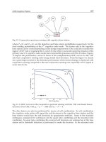
Arrays of washer-SQUIDs can be inductively coupled to a single multilayer flux transformer
having corresponding number of input coils and a sufficiently large inductance of the
transformer pick-up loop. We suggest to couple inductively dual-SQUIDs with large area
multilayer flux transformers (see Figure 12) for further improvement of the operation
parameters of the high-T
c
DC SQUID magnetometers and gradiometers.
Fig. 12. Schematics of the dual-SQUID flip-chip magnetometer with control electronics.
Applications of High-Tc Superconductivity
168
In the suggested dual-SQUID circuit, shown schematically in Figure 12, both SQUIDs are
directly coupled to a common pick-up loop, which, in turn, is inductively coupled to a
feedback and modulation coil of the control electronics. The two SQUID washers are also
inductively coupled to two multiturn input coils of the large-area multilayer flux
transformer providing sensitivity of the sensor to the magnetic field to be measured.
Application of the modulation signal to a directly coupled loop results in lower noise of the
sensor. In this case, the feedback modulation signals are essentially decoupled from the
pick-up loop of the multilayer flux transformer. This results in less cross-talk between the
sensors compared to the case of application of the modulation signal to the pick-up coil of
the multilayer flux transformer.
Further developments of the high-T
c
DC SQUID sensors will include, for example, large
multilayer flux transformers for more sensitive magnetometers and large-base-length
gradiometers; further reduction of low-frequency noise especially for SQUIDs exposed to
large permanent magnetic fields; Q-spoiler (Hilbert et al., 1985) or different types of
switches (Enpuku et al., 2001, 2002), which can be used for the dissipation of parasitic
circulating currents in the flux transformer during large changes of the external magnetic
fields. The switches allow sensitive measurements with the SQUID magnetometers shortly
after their movement in the Earth’s field or after the application of strong excitation fields
for low-field magnetic resonance measurements. This can be potentially used in low field
magnetic resonance measurement systems for spectroscopy, biology, or security
applications (Liao et al., 2010) (Espy et al., 2005, 2010).
5.5 Encapsulation of the high-T
c
DC SQUIDs
The high-T
c
SQUID sensors need to be encapsulated to ensure a long and reliable service
life. This is especially important for the flip-chip sensors with multilayer flux transformers.
The encapsulations provide mechanical and chemical protection of the sensors thus
significantly simplifying handling of the sensors during characterization, applications, and
for the end-users. The vacuum-tight sealing prevents the high-T
c
SQUID sensors from
degradation by ambient atmosphere and humidity.
The best results are obtained with enclosure of the sensors in fibreglass epoxy
encapsulations. Such packaging includes the SQUID with the multilayer flux transformer as
well as heater, RF filters, and a feedback coil. The thin-film Pt resistor PT-100 serves both as
a thermometer and as a heater. The heater allows easy removal of trapped magnetic flux to
improve the low frequency noise properties of the sensor. Good passivation was also
obtained by pouring high-T
c
DC SQUIDs into non-corrosive one- or two-component silicone
elastomers. However, the fibreglass capsule has the advantage that, if necessary, it can be
easily opened for correction or repair of the sensor followed by recapsulation.
The size and shape of the encapsulation are usually adapted to the sensor and to the specific
measuring systems intended for different applications. As examples, Figure 13 shows a
magnetometer and a gradiometer encapsulated into the fibreglass encapsulations. Typically,
the magnetometers and gradiometers are enclosed vacuum-tight in the button-shaped
encapsulations like the one shown in Figure 13a.
In the case of the flux transformers with sufficiently large-area pick-up loop, the fibre-glass
capsulation can have one or two holes (Fig.13b) with vacuum-tight walls inside to permit a
ferromagnetic antenna to freely tread through the pick-up coil of the thin-film flux
transformer to provide better coupling to an external magnetic flux source. Such cryogenic