Crystalline Silicon Properties and Uses Part 8 docx
Bạn đang xem bản rút gọn của tài liệu. Xem và tải ngay bản đầy đủ của tài liệu tại đây (1.85 MB, 25 trang )
Crystalline Silicon – Properties and Uses
164
Chiodini N. , Meinardi F. , Morazzoni F. , Paleari A. , Scotti R. and Martino D. Di. :
Ultraviolet photoluminescence of porous silica, Appl. Phys. Lett. 76 (2000) 3209.
Edwards A. H. , Fowler W. B. and Robertson J. : Structure and imperfections in amorphous and
crystalline silicon dioxide , R. Devine A. B. , Duraud J P. and Dooryhée E. (eds.),
John Wiley & Sons Ltd., (2000), p.253.
Fair R. B. : Physical models of boron diffusion in ultrathin gate oxides, J. Electrochem. Soc. 144
(1997) 708.
Fan X. D. , Peng J. L. and Bursill L. A. : Joint Density of States of Wide-Band-Gap Materials by
Electron Energy Loss Spectroscopy, Modern Phys. Lett. B 12 (1998) 541.
Fanderlik I. (ed.) : Silica Glass and its Application , Glass Science and Technology 11, ELSEVIER,
Amsterdam, (1991).
Feigl F. J. , Fowler W. B. and Yip K. L. : Oxygen vacancy model for the E'
1
center in SiO
2
,
Solid State Commun. 14 (1974) 225.
Feder R. , Spiller E. and Topalian J. : X-Ray Lithography, Polymer Eng. Sci. 17 (1977) 385.
Finlayson -Pitts B. J. and Pitts J. N. : Jr., Atmospheric Chemistry, Fundamental sand Experimental
Techniques, John Wiley, New York, (1986).
Fitting H J. , Ziems T. , von Czarnowski A. and Schmidt B. : Luminescence center
transformation in wet and dry SiO
2
, Radiation Measurements 39 (2004) 649.
Friebele E. J. , Griscom D. L. , Stapelbroek M. and Weeks R. A. : Fundamental Defect Centers in
Glass: The Peroxy Radical in Irradiated, High-Purity, Fused Silica, Phys. Rev. Lett. 42
(1979) 1346.
Friebele E. J. , Griscom D. L. and Marrone M. J. : The optical absorption and luminescence
bands near 2 eV in irradiated and drawn synthetic silica} , J. Non-Cryst. Solids 71
(1985) 133.
Fuchs E. , Oppolzer H. and Rehme H. : Particle Beam Microanalysis: Fundamental, Methods and
Applications, VCH Verlagsgesellschaft, Weinheim, (1990).
Gerber Th. and Himmel B. : The Structure of Silica Glass, J. Non-Cryst. Solids 83 (1986) 324.
Gendron-Badou A. , Coradin T. , Maquet J. , Fröhlich F. and Livage J. : Spectroscopic
characterization of biogenic silica, J. Non-Cryst. Solids 316 (2003) 331.
Glinka Y. D. , Lin S H. and Chen Y T. : The photoluminescence from hydrogen-related species in
composites of SiO
2
nanoparticles, Appl. Phys. Lett. 75 (1999) 778.
Glinka Y. D. : Two-photon-excited luminescence and defect formation in SiO
2
nanoparticles induced
by 6.4-eV ArF laser light, Phys. Rev. B 62 (2000) 4733.
Gobsch G. , Haberlandt H. , Weckner H J. and Reinhold J. : phys. stat. sol. (b) 90 (1978) 309.
Gorton N. T. , Walker G. , Burley, S. D. : Experimental analysis of the composite blue CL emission
in quartz - is this related to aluminium content? In: Abstracts SLMS International
Conference on Cathodoluminescence, Nancy, Sept (1996) , p.59.
Griggs D. T. and Blacic J. D. : Quartz : Anomalous weakness of synthetic crystals, Science
147 (1965) 292.
Griggs D. T. : Hydrolytic weakening of quartz and other silicates, Geophys. J. R. Astron. Soc. 14
(1967) 19.
Griscom D. L. , Friebele E. J. and Sigel G. H. : Observation and analysis of the primary 29Si
hyperfine structure of the E' center in non-crystalline SiO
2
, Solid State Commun. 15
(1974) 479.
Griscom D. L. : The electronic structure of SiO
2
: A review of recent spectroscopic and theoretical
advances, J. Non-Cryst. Solids 24 (1977) 155.
Defect Related Luminescence in Silicon Dioxide Network: A Review
165
Griscom D. L. : E' center in glassy SiO
2
: Microwave saturation properties and confirmation of the
primary
29
Si hyperfine structure, Phys. Rev. B 20 (1979a) 1823.
Griscom D. L. : Proc. 33rd Frequency Control Symposium (Elrctronic Indstrial Association,
Washington, DC, (1979b), p.98.
Griscom D. L. : E' center in glassy SiO
2
:
17
O,
1
H, and "very weak"
29
Si superhyperfine structure,
Phys. Rev. B 22 (1980) 4192.
Griscom D. L. , Stapelbroek M. and Friebele E. J. : ESR studies of damage processes in X-
irradiated high purity α-SiO
2
:OH and characterization of the formyl radical defect, J.
Chem. Phys. 78 (1983) 1638.
Griscom D. L. : Characterization of three E'-center variants in X- and γ-irradiated high purity a-
SiO
2
, Nucl. Instrum. and Methods Phys. Res. B 1 (1984) 481.
Griscom D. L. : Defect structure of glasses : Some outstanding questions in regard to vitreous silica,
J. Non-Cryst. Solids 73 (1985) 51.
Griscom D. L. and Friebele E. J. : Fundamental radiation-induced defect centers in synthetic fused
silicas: Atomic chlorine, delocalized E' centers, and a triplet state, Phys. Rev. B 34 (1986)
7524.
Griscom D. L. : Glass Science and Technology, D. R. Uhlmann and N. J. Kreidl (eds), Academic,
London, Vol. 4B (1990a) 151.
Griscom D. L. : Optical Properties and Structure of Defects in Silica Glass, J. of the Ceramic
Society of Japan 99 (1991) 899.
Griscom D. L. : The natures of point defects in amorphous silicon dioxide, Pacchioni et a. (eds.) ,
Defects in SiO
2
and related Dielectrics: Science and Technology, Kluwer Academic
Publishers, (2000), p.117.
Guzzi M. , Martini M. , Mattaini M. , Pio F. and Spenolo G. : Luminescence of fused silica:
Observation of the O
¯
2
emission band, Phys. Rev. B 35 (1987) 9407.
Hagni R. D. : Industrial applications of cathodoluminescence microscopy. In: Hagni R. D. (ed.):
Process Mineralogy IV: Applications to precious metal deposits, industrial minerals, coal,
liberation, mineral processing, agglomeration, metallurgical products, and refractories, with
special emphasis on cathodoluminescence microscopy. TMS, Warrendale, Pennsylvania,
(1987), p.37.
Hayes W. , Kane M. J. , Salminen O. , Wood R. L. and Doherty S. P. : ODMR of recombination
centres in crystalline quartz, J. Phys. C 17 (1984) 2943.
Hayes W. and Jenkin T. J. L. : Paramagnetic hole centres produced in germanium-doped crystalline
quartz by X-irradiation at 4K, J. Phys. C 18 (1985) L849.
Hayes W. and Stoneham A. M. : Defects and Defect Processes in Nonmetalic Solids, John Wiley,
New York, (1985).
Hayes W. and Jenkin T. J. L. : Optically detected magnetic resonance studies of exciton trapping by
germanium in quartz, J. Phys. C 21 (1988) 2391.
Heggie M. I. : A molecular water pump in quartz dislocations, Nature 355/23 (1992) 337.
Henderson G. S. and Baker D. R. (eds.) : Synchrotron Radiation: Earth, Environmental and
Material Sciences Applications, Short Course Series 30, Mineralogical Association of
Canada. (2002)159-178. Henderson G. S. , The Geochemical News, number 113,
October (2002), pp.13.
Hinic I. , Stanisic G. and Popovic Z. : Photoluminescence properties of silica aerogel during
sintering process, J. Sol-Gel Science and Technology 14 (1999) 281.
Crystalline Silicon – Properties and Uses
166
Hinic I. , Stanisic G. and Popovic Z. : Influence of the synthesis conditions on the
photoluminescence of silica gels, J. Serb. Chem. Soc. 68 (2003) 953.
Hosono H. , Abe Y. , Imagawa H. , Imai H. and Arai K. : Experimental evidence for the Si-Si
bond model of the 7.6-eV band in SiO2 glass, Phys. Rev. B 44 (1991) 12043.
Hosono H. , Abe Y. , Kinser D. L . , Weeks R. A. , Muta K. and Kawazoe H. : Nature and
origin of the 5-eV band in SiO
2
:GeO
2
glasses, Phy. Rev. B 46 (1992) 11445.
Hosono H. , Mizuguchi M. , Kawazoe H. and Ogawa T. : Effects of fluorine dimer excimer laser
radiation on the optical transmission and defect formation of various types of synthetic SiO
2
glasses, Appl. Phys. Lett. (1999) 2755.
Im S. , Jeong J. Y. , Oh M. S. , Kim H. B. , Chae K. H. , Whang C. N. and Song J. H. :
Enhancing defect-related photoluminescence by hot implantation into SiO
2
layers, Appl.
Phys. Lett. 47 (1999) 961
Imai H. , Arai K. , Saito T. , Ichimura S. Nonaka H. , Vigroux J. P. , Imagawa H. , Hosono H.
and Abe Y. : UV and VUV optical absorption due to intrinsic and laser induced defects in
synthetic silica glasses, in R. A. B. Devine (ed.), The physics and Technology of
Amorphous SiO
2
, Plenum, New York, (1987), p.153.
Imai H. , Arai K. , Imagawa H. , Hosono H. and Abe Y. : Two types of oxygen-deficient centers
in synthetic silica glass, Phys. Rev. B 38 (1988) 12772.
Imakita K. , Fujii M. , Yamaguchi Y. , and Hayashi S. : Interaction between Er ions and shallow
impurities in Si nanocrystals within SiO
2
, Phys. Rev. B 71 (2005) 115440.
Isoya J. , Weil J. A. and Hallibruton L. E. : EPR and ab initio SCF-MO studies of the Si·H—Si
system in the E'
4
center of α-quartz, J. Chem. Phys. 74 (1981) 5436.
Itoh C. , Tanimura K. and Itoh N. : Optical studies of self-trapped excitons in SiO
2
, J. Phys. C :
Solid State Phys. 21 (1988) 4693.
Itoh C. , Tanimura K. , Itoh N. and Itoh M. : Threshold energy for photogeneration of self-trapped
excitons in SiO
2
, Phys. Rev. B 39 (1989) 11183.
Itoh C. , Suzuki T. and Itoh N. : Luminescence and defect formation in undensified and densified
amorphous SiO
2
, Phys. Rev. B 41 (1990) 3794.
Kajihara K.,Skuja L.,Hirano M. and Hosono H.: Formation and decay of the nonbridging oxygen
hole centers in SiO
2
glasses induced by F
2
laser irradiation: In situ observation using a
pump and probe technique, Appl.Phys.Lett. 79 (2001) 1757.
Kajihara K. , Ikuta Y. , Hirano M. and Hosono H. : Effect of F
2
laser power on defect formation in
high-purity SiO
2
glass, J. Non-Cryst. Solids 322 (2003) 73.
Kajihara K. , Skuja L. , Hirano M. and Hosono H. : Role of Mobile Interstitial Oxygen Atoms in
Defect Processes in Oxides: Interconversion between Oxygen-Associated Defects in SiO
2
Glass, Phys. Rev. Lett. 92 (2004) 15504.
Kanemitsu Y. , Suzuki K. , Kondo M. and Matsumoto H. : Luminescence from a cubic silicon
cluster, Solid State Commun. 89 (1994) 619.
Khanlary M. R. , Townsend P. D. and Townsend J. E. : Luminescence spectra of germanosilicate
optical fibres.1: radioluminescence and cathodoluminescence, J. Phys. D 26 (1993) 371.
Khriachtchev L. , Räsänen M. , Novikov S. and Pavesi L. : Systematic correlation between
Raman spectra, photoluminescence intensity, and absorption coefficient of silica layers
containing Si nanocrystals, Appl. Phys. Lett. 85 (2004) 1511.
Kim H. B. , Son J. H. , Whang C. N. , Chae K. H. , Lee W. S. , Im S. , Kim S. O. , Woo J. J. and
Song J. H. : Light-Emitting Properties of Si-Ion-Irradiated SiO
2
/Si/SiO
2
Layers, J. the
Korean Phys. Soci. 37 (2000a) 466.
Defect Related Luminescence in Silicon Dioxide Network: A Review
167
Kim H. B. , Son J. H. , Chae K. H. , Jeong J. Y. , Lee W. S. , Im S. , Song J. H. and Whang C. N.
: Photoluminescence from Si ion irradiated SiO
2
Si SiO
2
films with elevated substrate
temperature, Materials Science and Engineering B 69-70 (2000b) 401.
Kim H. B. , Kim T. G. , Son J. H. , Whang C. N. , Chae K. H. , Lee W. S. , Im S. and Song J. H. ,
Effects of Si-dose on defect-related photoluminescence in Si-implanted SiO
2
layers, J. Appl.
Phys. 88 (2000c) 1851.
Kofstad P. : High Temperature Corrosion, ELSEVIER, London and New York, (1988).
Koyama H. : Cathodoluminescence study of SiO
2
, J. Appl. Phys. 51 (1980) 2228.
Krbetschek M. R. , Götze J. , Dietrich A. and Trautmann T. : Spectral Information from Minerals
Relevant for Luminescence Dating, Radiation Measurements 27 (1997) 695.
Kronenberg A. K. , Kirby S.H. , Aines R. D. and Rossmann G. R. : Solubility and diffusional
uptake of hydrogen in quartz at high water pressure: implications for hydrolytic weakening
in the laboratory and within the earth, Tectonophysics 172 (1986) 255.
Kuzuu N. and Murahara M. : X-ray-induced absorption bands in type-III fused silicas, Phys. Rev.
B 46 (1992) 14486.
Lamkin M. , Riley F. and Fordham R. : Oxygen Mobility in Silicon Dioxide and Silicate Glasses:
A Review, J. Eur. Ceram. Soc. 10 (1992) 347.
Lau H. W. , Tan O. K. , Liu Y. , Ng C. Y. , Chen T. P. , Pita K. and Lu D. : Defect-induced
photoluminescence from tetraethylorthosilicate thin films containing mechanically milled
silicon nanocrystals, J. Appl. Phys. 97 (2005) 104307.
Ledoux G. , Gong J. , Huisken F. , Guillois O. and Reynaud C. : Photoluminescence of size-
separated silicon nanocrystals: Confirmation of quantum confinement, Appl. Phys. Lett.
80 (2002) 4834.
Lee W. S. , Jeong J. Y. , Kim H. B. , Chae K. H. , Whang C. N. , Im S. and Song J. H. : Violet
and orange luminescence from Ge-implanted SiO
2
layers, Materials Science and
Engineering B 69-70 (2000) 474.
Lide D. R. : CRC Handbook of Chemistry and Physic, 85th edition, CRC Press, (2004).
Lu Z. Y. , Nicklaw C. J. , Fleetwood D. M. , Schrimpf R. D. and Pantelides S. T. : Structure,
Properties, and Dynamics of Oxygen Vacancies in Amorphous SiO
2
, Phys. Rev. Lett. 89
(2002) 285505.
Ludwig M. H. , Menniger J. , Hummel R. E. : Cathodoluminescing properties of spark-processed
silicon, J. Phys: Condens. Matter 7 (1995) 9081
Luff B. J. and Townsend P. D. : Cathodoluminescence of synthetic quartz, J. Phys. Condensed
Matter 2 (1990) 8089.
Magruder R. H. , Weeks R. A. and Weller R. A. : Luminescence and absorption in type III silica
implanted with multi-energy Si, O and Ar. ions, J. Non-Cryst. Solids 322 (2003) 58.
Majid F. B. and Miyagawa I. : Detection of Several Types of E'-center by ESR Double Modulation
Spectrum Method, Chem. Phys. Lett. 209 (1993) 496.
Marshall D. J. : Cathodoluminescence of geological materials, Allen & Unwin Inc., Winchester
Mass., (1988).
McLaren A. C. , Cook R. F. , Hyde S. T. , Tobin R. C. : The mechanisms of the formation and
growth of water bubbles and associated dislocation loops in synthetic quartz, Phys. Chem.
Minerals 9 (1983) 79.
Mitchell J. P. and Denure D. G. : A study of SiO layers on Si using cathodoluminescence spectra,
Solid State Electron. 16 (1973) 825.
Crystalline Silicon – Properties and Uses
168
Mohanty T. , Mishra N. C. , Bhat S. V. , Basu P. K. and Kanjilal D . : Dense electrnic excitation
induced defects in fused silica, J. Phys. D: Appl. Phys. 36 (2003) 3151.
Morimoto Y. , Igarashi T. , Sugahara H. and Nasu S. : Analysis of gas release from vitreous silica,
J. Non-Cryst. Solids 139 (1992) 35.
Morimoto Y. , Weeks R. A. , Barnes A. V. , Tolk N. H. and Zuhr R. A. : The effect of ion
implantation on luminescence of a silica, J. Non-Cryst. Solids 196 (1996) 106.
Mozzi R. L. and Warren B. E. : The Structure of Vitreous Silica, J. Appl. Crystallogr. 2 (1969)
164.
Munekuni S. , Yamanaka T. , Shimogaichi Y. , Tohmon R. , Ohki Y. , Nagasawa K. and
Hama Y. : Various types of nonbridging oxygen hole center in high-purity silica glass, J.
Appl. Phys. 68 (1990) 1212.
Mysovsky A. S. , Sushko P. V., Mukhopadhyay S. , Edwards A. H. and Shluger A. L.:
Calibration of embedded-cluster method for defect studies in amorphous silica, Phys. Rev.
B 69 (2004) 85202.
Nicholas J. B. , Hopfinger A. J. , Trouw F. R. and Iton E. : Molecular Modeling of Zeolite
Structure. 2. Structure and Dynamics of Silica Sodalite and Silicate Force Field, J. Am.
Chem. Soc. 113 (1991) 4792.
Nicollian E. H. and Brews J. R. : MOS (Metal Oxide Semiconductor) Physics and Technology,
WILEY-VCK, New York, (2002).
Nishikawa H. , Shiroyama Y. , Nakamura R. , Ohki Y. , Nagasawa K. and Hama Y.:
Photoluminescence from defect centers in high-purity silica glasses observed under 7.9-eV
excitation, Phys. Rev. B 45 (1992) 586.
Nishikawa H. , Watanabe E. , Ito D. and Ohki Y. : Decay kinetics of the 4.4 eV
photoluminescence associated with the two states of oxygen-deficient-type defect in
amorphous SiO
2
, Phys. Rev. Lett. 72 (1994) 2101.
Nishikawa H. : Structure and properties of amorphous silicon dioxide-Isuse on the reliability and
novel applications, Chapter 3 pp.93 in: Hari Singh Nalwa, Silicon-Based Materials
and Devices, Vol. 2, (2001).
Nuttall R. H. D. and Weil J. A. : Two hydrogenic trapped-hole species in α-quartz, Solid State
Commun. 33 (1980) 99.
O'Reilly E. P. and Robertson J. : Theory of defects in vitreous silicon dioxide, Phys. Rev. B 27
(1983) 3780.
Ozawa L. : Cathodoluminescence: Theory and Application , Kodansha Ltd., Japan, (1990).
Pacchioni G. and Ierano G. : Optical Absorption and Nonradiative Decay Mechanism of E' Center
in Silica, Phys. Rev. Lett. 81 (1998a) 377.
Pacchioni G. and Ierano G. : Ab initio theory of optical transitions of point defects in SiO
2
, Phys.
Rev. B 57 (1998b) 818.
Pacchioni G. , Skuja L. and Griscom D. L. : Defects in SiO
2
and related dielectrics: Science and
technology, (2000), p.73.
Paleari A. , Chiodini N. , Di Martino D. and Meinardi F. : Radiative decay of vacuum-ultraviolet
excitation of silica synthesized by molecular precursors of Si-Si sites: An indicator of
intracenter relaxation of neutral oxygen vacancies, Phys. Rev. B 71 (2005) 75101.
Pellergrino P. , Perez-Rodriguez A. , Garrido B. , Gonzalez-Varona O. , Morante J. R.,
Marcinkevicius S. , Galeckas A. and Linnros J. : Time-resolved analysis of the white
photoluminescence from SiO
2
films after Si and C coimplantation, Appl. Phys. Lett. 84
(2004) 25.
Defect Related Luminescence in Silicon Dioxide Network: A Review
169
Perez-Rodriguez A. , Gonzalez-Varona O. , Garrido B. , Pellegrino P. , Morante J. R., Bonafos
C. , Carrada M. and Claverie A. : White luminescence from Si
+
and C
+
ion-implanted
SiO
2
films, J. Appl. Phys. 94 (2003) 254.
Plaksin O. A. , Takeda Y. , Okubo N. , Amekura H. , Kono K. , Umeda N. , Kishimoto N. :
Electronic transitions in silica glass during heavy-ion implantation, Thin Solid Films 464-
465 (2004) 264.
Prado R. J. , D'Addio T. F. , Fantini M. C. A. , Pereyra I. and Flank A. M. : Annealing effects of
highly homogeneous a-Si
1-x
C
x
:H, J. Non-Cryst. Solids 330 (2003) 196.
Qin G. G. , Lin J. , Duan J. Q. and Yao G. Q. : A comparative study of ultraviolet emission with
peak wavelengths around 350 nm from oxidized porous silicon and that from SiO
2
powder,
Appl. Phys. Lett. 69 (1996) 1689.
Rafferty C. S. : Stress Effects in Silicon Oxidation Simulation and Experiments, PhD thesis ,
Stanford University, (1989).
Rebohle L. , Gebel T. , Fröb H. , Reuther H. and Skorupa W. : Ion beam processing for Si/C-rich
thermally grown SiO
2
, Appl. Surf. Sci. 184 (2001a) 156.
Rebohle L. , Gebel T. , von Borany J. , Skorupa W. , Helm M. , Pacifici D. , Franzo G. and
Priolo F. : Transient behavior of the strong violet electroluminescence of Ge-implanted SiO
2
layers, Appl. Phys. B 74 (2002a) 53.
Rebohle L. , von Borany J. , Fröb H. , Gebel T. , Helm M. and Skorupa W. : Ion beam
synthesized nanoclusters for silicon-based light emission, Nucl. Instrum. Methods Phys.
Res. B 188 (2002b) 28.
Reimer L. : Scanning Electron Microscopy: Physics of Image Formation and Microanalysis,
Springer series in optical sciences, Vol. 45, (1998).
Robertson J. : The Physics and Technology of Amorphous SiO
2
, Roderich A. B. Devine (ed.),
National center for Telecommunication Studies, Meyland, France, (1988).
Rudra J. K. , Fowler B. W. and Feigl F. J. : Model for the E'
2
center in Alpha Quartz , Phys. Pev.
Lett. 55 (1985) 2614.
Saito K. and Ikushima A. J. : Effects of fluorine on structure, structural relaxation, and absorption
edge in silica glass, J. Appl. Phys. 91 (2002) 4886.
Sakurai Y. , Nagasawa K. , Nishikawa H. and Ohki Y. : Characteristic red photoluminescence
band in oxygen-deficient silica glass, J. Appl. Phys. 86 (1999) 370.
Sakurai Y. : Oxygen-related red photoluminescence bands in silica glasses, J. Non-Cryst. Solids 316
(2003) 389.
Seol K. S. , Ohki Y. , Nishikawa H. , Takiyama M. and Hama Y. : Effect of implanted ion species
on the decay kinetics of 2.7 eV photoluminescence in thermal SiO
2
films, J. Appl. Phys. 80
(1996) 6444.
Settle F. A. (ed.) : Handbook of Instrumental Techniques for Analytical Chemistry, Prentice Hall,
(1997).
Shimizu-Iwayama T. , Ohshima M. , Niimi T. , Nakao S. , Saitoh K. , Fujita T. and Itoh N. :
Visible photoluminescence related to Si precipitates in Si
+
-implanted SiO
2
, J. Phys.:
Condens. Matter 5 (1993) L375.
Shimizu-Iwayama T. , Nakao S. and Saitoh K. : Optical and structural characterization of
implanted nanocrystalline semiconductors, Nucl. Instrum. Methods Phys. Res. B 121
(1997) 450.
Skuja L. , Streletsky A. N. and Pakovich A. B. : A new intrinsic defect in amorphous SiO
2
:
Twofold coordinated silicon, Solid State Commun. 50 (1984) 1069.
Crystalline Silicon – Properties and Uses
170
Skuja L. and Trukhin A. : Comment on " Luminescence of fused silica: Observation of the O
¯
2
emission band, Phys. Rev. B 39 (1989) 3909.
Skuja L. : Isoelectronic series of twofold coordinated Si, Ge, and Sn atoms in glassy SiO
2
: a
luminescence study, J. Non-Cryst. Solids 149 (1992a) 77.
Skuja L. : Time-resolved low temperature luminescence of non-bridging oxygen hole centers in silica
glass, Solid State Commun. 84 (1992b) 613.
Skuja L. : The origin of the 1.9eV luminescence band in glassy SiO
2
, J. Non-Cryst. Solids 179
(1994a) 51.
Skuja L. , Suzuki T. , Tanimura K. : Site-selective laser-spectroscopy studied of the intrinsic 1.9-eV
luminescence center in glassy SiO
2
, Phys. Rev. B 52 (1995) 15208.
Skuja L. : Optically active oxygen-deficiency-related centers in amorphous silicon dioxide, J. Non-
Cryst. Solids 239 (1998) 16.
Skuja L. , Güttler B. , Schiel D. and Silin A. R. : Quantitative analysis of the concentration of
interstitial O
2
molecules in SiO
2
glass using luminescence and Raman spectroscopy, J.
Appl. Phys. 83 (1998a) 6106.
Skuja L. , Güttler B. , Schiel D. and Silin A. R. : Infrared photoluminescence of preexisting or
irradiation-induced interstitial oxygen molecules in glassy SiO
2
and α-quartz, Phys. Rev B
58 (1998b) 14296.
Skuja L. , Optical properties of defects in silica, pp.73-116 in Pacchioni G., Skuja L. and Griscom
D. L. (eds) : Defects in SiO
2
and related dielectrics: Science and technology, (2000).
Skuja L. , Hirano M. and Hosono H. : Oxygen-Related Intrinsic Defects in Glassy SiO
2
:
Interstitial Ozone Molecules, Phys. Rev. Lett. 84 (2000a) 302.
Skuja L. , Mizuguchi M. , Hosono H. and Kawazone H. : The nature of the 4.8 eV optical
absorption band induced by vacuum-ultraviolet irradiation of glassy SiO
2
, Nucl. Instrum.
Methods Phys. Res. B 166-167 (2000b) 711.
Skuja L. , Kajihara K. , Kinoshita T. , Hirano M., Hosono H. : The behavior of interstitial oxygen
atoms induced by F
2
laser irradiation of oxygen-rich glassy SiO
2
, Nucl. Instr. & Methods
in Physics Research B 191 (2002) 127.
Skuja L. , Kajihara K. , Hirano M. , Saitoh A. , Hosono H. : An increased F
2
-laser damage in
'wet' silica glass due to atomic hydrogen: A new hydrogen-related E'-center, J. Non-Cryst.
Solids 352 (2006) 2297.
Slater J. C. : Quantum Theory of Molecules and Solids: Symmetry and Energy Bands in Crystals,
McGraw-Hill, New York, Vol. 2, (1965).
Snyder K. C. and Fowler W. B. : Oxygen vacancy in α-quartz: A possible bi- and metastable defect,
Phys Rev. B 48 (1993) 13238.
Song J. , Corrales L. R. , Kresse G. and Jonsson H. : Migration of O vacancies in alpha-quartz:
The effect of excitons and electron holes, Phys. Rev. B 64 (2001) 134102.
Song K. S. and Williams R. T. : Self-Trapped Excitons, Springer Verlag, Berlin, (1993).
Stapelbroek M. , Griscom D. L. , Friebele E. J. and Sigel Jr. G. H. : Oxygen-associated trapped-
hole centers in high-purity fused silicas, J. Non-Cryst. Solids 32 (1979) 313.
Stevens-Kalceff M. A. and Philips M. R. : Cathodoluminescence microcharacterization of the defect
structure of quartz, Phys. Rev. B 52 (1995) 3122.
Stevens-Kalceff M. A. : Cathodoluminescence microcharacterization of the defect structure of
irradiated hydratedand anhydrous fused silicon dioxide, Phys. Rev. B 57 (1998) 5674.
Stevens-Kalceff M. A. : Electron-Irradiation-Induced Radiolytic Oxygen Generation and
Microsegregation in Silicon Dioxide Polymorphs, Phys. Rev. Lett. 84 (2000) 3137.
Defect Related Luminescence in Silicon Dioxide Network: A Review
171
Stevens-Kalceff M. A. , Stesmans A. and Wong J. : Defects induced in fused silica by high fluence
ultraviolet laser pulses at 355 nm, Appl. Phys. Lett. 80 (2002) 758.
Stevens-Kalceff M. A. and Wong J. : Distribution of defects induced in fused silica by ultraviolet
laser pulses before and after treatment with a CO
2
laser, J. Appl. Phys. 97 (2005) 113519.
Streletsky A. N. , Pakovich A. B. , Gachkovski V. F. , Aristov Yu. I. , Rufov Yu. N. and
Butyagin P. Y. : Khim. Fizika, Sov. Chem. Phys., No.7 (1982) 938.
Suzuki T. , Skuja L. , Kajihara K. , Hirano M. , Kamiya T. and Hosono H. : Electronic
Structure of Oxygen Dangling Bond in Glassy SiO
2
: The Role of Hyperconjugation, Phys.
Rev. Lett. 90 (2003) 186404.
Takagahara T. and Takeda K. : Theory of the quantum confinement effect on excitons in quantum
dots of indirect-gap materials, Phys. Rev. B 46 (1992) 15578.
Tanimura K. , Tanaka T. and Itoh N. : Creation of Quasistable Lattice Defects by Electronic
Excitation in SiO
2
, Phys. Rev. Lett. 51 (1983) 423.
Tong S. , Liu X N. , Gao T. and Bao X M. : Intense violet-blue photoluminescence in as-deposited
amorphous Si:H:O films, Appl. Phys. Lett. 71 (1997) 698.
Trukhin A. N. : Investigation of the Photoelectric and Photoluminescent Properties of Crystalline
Quartz and Vitreous Silica in the Fundamental Absorption Region, phys. stat. sol. (b) 86
(1978) 67.
Trukhin A. N. and Plaudis A. E. : Investigation of intrinsic luminescence of SiO
2
, Sov. Phys.
Solid State 21 (1979) 644.
Trukhin A. N. : Studey of Exitons in SiO
2
- Luminescent Centers as Exciton Detectors, phys. stat.
sol. (b) 98 (1980) 541.
Trukhin A. N. : Excitons in SiO
2
: a review, J. Non-Cryst. Solids 149 (1992) 32.
Trukhin A. N. : Luminescence of a self-trapped exciton in GeO
2
crystal, Solid State Commun. 85
(1993) 723.
Trukhin A. N. : Self-trapped exciton luminescence in α-quartz, Nucl. Instr. and Meth. in Phys.
Res. B 91 (1994) 334.
Trukhin A. N. , Goldberg M. , Jansons J. , Fitting H J. and Tale I. A. : Silicon dioxide thin film
luminescence in comparison with bulk silica, J. Non-Cryst. Solids 223 (1998) 114.
Trukhin A. N. and Fitting H J. : Investigation of optical and radiation properties of oxygen
deficient silica glasses, J. Non-Cryst. Solids 248 (1999) 49.
Trukhin A. N. , Jansons J. , Fitting H J. , Barfels T. and Schmidt B. : Cathodoluminescence decay
kinetics in Ge
+
, Si
+
, O
+
implanted SiO
2
layers, J. Non-Cryst. Solids 331 (2003a) 91.
Trukhin A. , Poumellec B. and Garapon J. : Study of the germanium luminecence in silica: from
non-controlled impurity to germano-silicate core of telecommunication fiber performs , J.
Non-Cryst. Solids 332 (2003b) 153.
Trukhin A. and Poumellec B. : Photosensitivity of silica glass with germanium studied by
photoinduced of thermally stimulated luminescence with vacuum ultraviolet radiation, J.
Non-Cryst. Solids 324 (2003c) 21.
Tsu D. V. , Lucovsky G. and Davidson B. N. : Effects of the nearest neighbors and the alloy matrix
on SiH stretching vibrations in the amorphous SiO
r
:H (0<r<2) alloy system, Phys. Rev. B
40 (1989) 1795.
Uchino T. , Takahashi M. and Yoko T. : Model of oxygen-deficiency-related defects in SiO
2
glass,
Phys. Rev. B 62 (2000b) 2983.
Uchino T. , Takahashi M. and Yoko T. : Structure and Generation Mechanism of the Peroxy-
Radical Defect in Amorphous Silica, Phys. Rev. Lett. 86 (2001) 4560.
Crystalline Silicon – Properties and Uses
172
van Santen R. A. , de Man A. J. M. , Jacobs W. P. J. H. , Teunissen E. H. and Kramer G. J. :
Lattice Relaxation of Zeolites, Catalysis Letters 9 (1991) 273.
Weeks R. A. : Paramagnetic Resonance of Lattice Defects in Irradiated Quartz, J. Appl. Phys. 27
(1956) 1376.
Weeks R. A. and Nelson C. M. : Trapped electrons in irradiated quartz and silica. I. Optical
absorption, J. Am. Ceram. Soc. 43 (1960) 399.
Weeks R. A. : Paramagnetic Spectra of E´2 Centers in Crystalline Quartz, Phys. Rev. 130 (1963) 570.
Weeks R. A. , Magruder R.H. , Gaylon R. and Weller R.A. : Effects of B and N implantation on
optical absorption and photoluminescence and comparison to the effects of implanting Si,
Ge, O, and Ar in silica, J. Non-Cryst. Solids 351 (2005) 1727.
Weber J. T. and Cromer D. T. : Orbital Radii of Atoms and Ions, J. Chem. Phys. 42 (1965) 4116.
Wilkinson A. R. and Elliman R. G. : The effect of annealing environment on the luminescence of
silicon nanocrystals in silica, J. Appl. Phys. 96 (2004) 4018.
White B. D. , Brillson L. J. , Bataiev M. , Brillson L. J. , Fleetwood D. M. , Schrimpf R. D. ,
Choi B. K. , Fleetwood D. M. and Pantelides S. T. : Detection of trap activation by
ionizing radiation in SiO
2
by spatially localized cathodoluminescence spectroscopy, J. Appl.
Phys. 92 (2002) 5729.
Yacobi B. G. and Holt D. B. : Cathodoluminescence Microscopy of Inorganic Solids, Plenum Press,
New York and London, (1990).
Yang X. H. , Townsend P. D. and Holgate S. A. : Cathodoluminescence and depth profiles of tin
in float glass , J. Phys. D 27 (1994) 1757.
Yang X. , X. , Wua L. , Li S. H. , Li H. , Qiu T. , Yang Y. M. , Chu P. K. and Siu G. G. : Origin of
the 370-nm luminescence in Si oxide nanostructures , Appl. Phys. Lett. 86 (2005) 201906.
Yao B. , Shi H. , Zhang X. and Zhang L. : Ultraviolet photoluminescence from nonbridging oxygen
hole centers in porous silica, Appl. Phys. Lett. 78 (2001) 174.
Yi L. X. , Heitmann J. , Scholz R. and Zacharias M. : Si rings, Si clusters, and Si nanocrystals-
different states of ultrathin SiO
x
layers, Appl. Phys. Lett. 81 (2002) 4248.
Yi L. X. , Heitmann J. , Scholz R. and Zacharias M. : Phase separation of thin SiO layers in amorphous
SiO/SiO
2
superlattice during annealing, J. Phys. : Condens. Matter 15 (2003) S2887.
Yip K. L. and Fowler W. B. : Electronic structure of E'
1
centers in SiO
2
, Phys. Rev. B 11 (1975) 2327.
Yu Z. , Aceves M. , Carrillo J. , Flores F. , Falcony C. , Domínguez C. , Llobera A. and
Morales-Acevedo A. : Photoluminescence in off-stoichiometric silicon oxide compounds,
Superficies y Vacio 17 (2004) 1.
Zacharias M. , Tsybeskov L. , Hirschman K. D. , Fauchet P. M. , Bläsing J. , Kohlert P. and
Veit P. : Nanocrystalline silicon superlattices: fabrication and characterization, J. Non-
Cryst. Solids 227-230 (1998) 1132.
Zacharias M. , Heitmann J. , Scholz R. , Kahler U. , Schmidt M. and Bläsing J. : Size-controlled
highly luminescent silicon nanocrystals: A SiO/SiO
2
superlattice approach, Appl. Phys.
Lett. 80 (2002) 661.
Zacharias M. , Yi L. X. , Heitmann J. , Scholz R. , Reiche M. and Gösele U. : Size-controlled Si
nanocrystals for photonic and electronic applications, Solis State Phenomena 94 (2003) 95.
Zatsepin A. F. , Biryukov D. Yu. and Kortov V. S. : Analysis of OSEE Spectra of Irradiated
Dielectrics, Latvian Journal of Physics and Technical Sciences. No.6 (2000) 83.
Zhang B. L. and Raghavachari K. : Photoabsorption and photoluminescence of divalent defects in
silicate and germanosilicate glasses: First-principles calculations, Phys. Rev. B 55 (1997),
15993.
Zunger A. and Wang L W. : Theory of silicon nanostructures , Appl. Surf. Sci. 102 (1996) 350.
9
Silicon Nanocluster in Silicon
Dioxide: Cathodoluminescence,
Energy Dispersive X-Ray Analysis
and Infrared Spectroscopy Studies
Roushdey Salh
Institute of Physics, Faculty of Science and Technology, Umeå University, Umeå
Sweden
1. Introduction
This chapter is extended to various electronical and optical modifications of amorphous
silica (a-SiO
2
) layers as they are applied in microelectronics, optoelectronics, as well as in the
forthcoming photonics. Scanning electron microscopy (SEM), energy dispersive X-ray
analysis (EDX), Fourier transform infrared spectroscopy (FTIR) and cathodoluminescence
(CL) have been used to investigate thermally grown pure amorphous silicon dioxide and
ion-implanted layers with thickness d
ox
=100-500 nm. The main luminescent centers in silicon
dioxide layers are the red luminescence (650 nm; 1.85 eV) of the non-bridging oxygen hole
center (NBOHC; ≡Si–O•), a blue (460 nm; 2.7 eV) and a ultra violet luminescence (290 nm;
4.3 eV) of the oxygen deficient centers (ODC's; ≡Si···Si≡), and a yellow luminescence (570
nm; 2.2 eV) appears especially in hydrogen treated silica indicating water molecules, and on
the other hand, in silicon excess samples indicating higher silicon aggregates. A quite
different CL dose behavior of the red luminescence is observed in dry and hydrogen-treated
samples due to dissociation and re-association of mobile hydrogen and oxygen to radicals of
the silica network. Additionally implanted hydrogen diminishes the red luminescence in
wet oxide but maintains the blue and the UV bands. Thus hydrogen passivates the NBOHC
and keeps the ODC's in active emission states. A model of luminescence center
transformation is proposed based on radiolytic dissociation and re-association of mobile
oxygen and hydrogen at the centers as well as formation of interstitial H
2
, O
2
, and H
2
O
molecules.
Non-stoichiometric SiO
x
layers produced by direct ion implantation or reactive sputtering
are used to investigate whether the different luminescent centers are related to oxygen or to
silicon. Oxygen implantation as well as direct silicon implantation led to an oxygen surplus
as well as an oxygen deficit, respectively. The related luminescence damages provide direct
evidence to the nature of the defects. Oxygen-deficient thin silica layers SiO
x
with different
stoichiometric degree 1≤x≤2, were prepared by thermal evaporation of silicon monoxide in
vacuum and in ambient oxygen atmosphere of varying pressure onto crystalline silicon
substrates. The chemical composition has been calibrated and determined by FTIR
spectroscopy. The CL spectra of the oxygen-deficient layers shows the development of
typical silica luminescence bands at the composition threshold x≤1.5 onwards to x=2. The
Crystalline Silicon – Properties and Uses
174
green-yellow luminescence (2.15 eV) strongly increases with the annealing temperature up
to 1300 °C which is attributed to the formation of small silicon aggregates in the network,
from dimers over trimers even to hexamer rings.
Ion implantation doses between 3×10
16
and 5×10
16
ions/cm
2
led to an atomic dopant fraction
of about 4 at.% at the half depth of the SiO
2
layers. In ion implanted SiO
2
layers additional
emission bands are observed. A huge violet band in Ge
+
implanted layers appears at λ=410
nm (3.1 eV). This band corresponds to the Ge-related oxygen deficient center (Ge-ODC). The
thermal annealing process of the Ge
+
implanted layers leads first to a strong increase of the
violet luminescence due to formation of Ge dimers, trimers or higher aggregates, finally to
destruction of the luminescence centers by further growing to Ge nanoclusters. Scanning
transmission electron microscopy (STEM) shows the growing in Ge cluster size with
increasing annealing temperature up to 1100 °C. As a result of ion implantation, we can state
that; group IV elements (C, Si, Ge, Sn, Pb) in SiO
2
increase the intensity of the luminescence
in the blue region and group VI elements (O, S, Se) increase the intensity in the red region,
confirming the association of the defect centers in the blue and the red region with oxygen
deficient centers and oxygen excess centers, respectively. The cathodoluminescence spectra
of sulfur-implanted SiO
2
layers and oxygen implanted layers under special conditions show
besides the characteristic luminescence bands a multimodal structure beginning in the green
region at 500 nm over the yellow-red region and extending to the near IR measured up to
820 nm. The energy step differences of the sublevels amount to an average 120 meV and
indicate vibronic-electronic transitions, probably of O
¯
2
interstitial molecules, which could
be demonstrated by a respective configuration coordinate model.
2. CL of stoichiometric and non-stoichiometric SiO
2
2.1 Wet and dry SiO
2
layers
The CL spectra of pure SiO
2
consist of several broad bands and certainly of some
overlapped components especially at the region around λ≈ 460-620 nm (2.7-2.0 eV). The
irradiation response of these luminescence bands indicates that they are associated with
different defect centers. Even at specimen temperatures as low as LNT where thermal
contributions to the bandwidth are almost minimized, the SiO
2
CL emission bands are still
broad because of the degree of coupling between the host lattice and the defects associated
with the luminescence emissions [Griscom 1990b].
The initial (1 sec) and the saturated (5 h) CL spectra of pure SiO
2
layers are presented
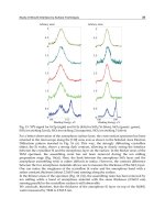
in Fig. 2.1. The main CL emission bands in wet and dry specimens at temperatures between
liquid nitrogen (LNT) and room temperature (RT) are the red luminescence R at 650 nm
(1.9 eV) associated with the NBOHC [Fitting et al. 2005b], the blue B and ultraviolet
UV bands at 460nm (2.7 eV) and 290 nm (4.3 eV) respectively, associated with the Si related
oxygen deficient center (Si-ODC) [Skuja 1994b]. Some shoulders can be also seen in
the green-yellow G-Y region between 500-580 nm (2.5-2.1 eV). A luminescence band at
500 nm (2.5 eV) in crystalline SiO
2
and another at 560 nm (2.2 eV) in amorphous SiO
2
is often
ascribed to the self trapped exciton (STE) [Skuja et al. 1978, Trukhin et al. 1998]. Another
CL band which is not often discussed in the literature is easily seen in the yellow Y region at
λ≈570-580 nm (2.18-2.14 eV) especially at LNT, but it is also expected in RT spectra where
the plane between the B band and the R bands can accommodate more than one overlapped
emission band.
Silicon Nanocluster in Silicon Dioxide: Cathodoluminescence,
Energy Dispersive X-Ray Analysis and Infrared Spectroscopy Studies
175
G
UV
B
R
RT
initial spectra (1 sec)
wet SiO : = 250 nm
dry SiO : = 200 nm
2
ox
2
ox
d
d
RT
initial
spectra (1 sec)
6 5 4 3 2.5 2 1.8 1.6
energy (eV)
UV
B
R
6 5 4 3 2.5 2 1.8 1.6
energy (eV)
CL-intensity (a.u.)
0
100
200
300
400
500
600
wet
dry
wet
dry
RT
saturated spectra (5 h)
wet SiO : = 250 nm
dry SiO : = 200 nm
2
ox
2
ox
d
d
RT
saturated spectra
(5 h)
200 300 400 500 600 700 800
G
UV
B
R
LNT
initial spectra (1 sec)
wet SiO : = 250 nm
dry SiO : = 200 nm
2
ox
2
ox
d
d
LNT
initial
spectra (1 sec)
wavelength (nm)
UV
B
R
wavelength (nm)
200 300 400 500 600 700 800
CL-intensity (a.u.)
0
100
200
300
400
500
600
wet
dry
wet
dry
LNT
saturated spectra (5 h)
wet SiO : = 250 nm
dry SiO : = 200 nm
2
ox
2
ox
d
d
LNT
saturated spectra
(5 h)
Y
Y
0
100
200
300
400
500
600
0
100
200
300
400
500
600
initial spectra saturated spectrainitial spectra saturated spectra
Fig. 2.1 The initial (1sec) and saturated (5h) CL spectra of wet and dry SiO
2
at room
temperature (RT) and liquid nitrogen temperature (LNT); electron beam energy E
o
=10 keV
and current density j
o
=5.4 mA/cm
2
.
CL bands in this region will be discussed in more detail in the following sections. Based on
our basic experimental observations we presume a very thin ice (H
2
O) layer to have been
produced on the surface of the sample as an effect of low temperatures which could be one
of the reasons for the Y band, but under any circumstances one can see that the local
intrinsic defects like ODC and NBOHC dominates the CL spectrum at LNT too.
Looking to the 1 sec spectra of both wet and dry SiO
2
in Fig. 2.1, we can state that some of
the detected luminescence bands have the same origin and they behave similarly under
electron beam irradiation but others are totally different or are formed/transformed by
more complex reactions. The UV luminescence always peaks at very low intensities which
scarcely change under irradiation. This band was not detected in many crystalline SiO
2
modifications at room temperature even or at liquid nitrogen temperature [Barfels 2001] but
it is clearly seen in bulk and thin layers of amorphous SiO
2
[Trukhin et al. 1998,
Bakaleinikov et al. 2004]. Absence of the crystalline order seems to be the origin of the UV
luminescence band. The blue B luminescence starts with the same intensity in both dry and
wet at RT and LNT and reaches the saturation level (5 h) together. The B band grows
drastically during the irradiation at room temperature (RT), while it is expected that a high
energetic electron beam creates more oxygen vacancy or in other words oxygen deficient
centers (ODC).
The main difference between the CL spectra of wet and dry SiO
2
is located in the Y and R
region. The Y luminescence is detected with relatively higher intensity in wet SiO
2
at RT and
Crystalline Silicon – Properties and Uses
176
it is more visible at LNT in both dry and wet SiO
2
which is probably associated with some
crystalline H
2
O molecules on the sample surface. A considerable increase in the R band
intensity is clearly seen in the initial spectra in wet SiO
2
. This is the main dissimilar point
between dry and wet oxide layers. We suspect a direct connection of the Y and R bands with
atomic or molecular hydrogen. The saturated spectra of wet and dry SiO
2
have almost the
same profile, see Fig. 2.1. That means, the red luminescence is starting from different
precursors in dry and wet SiO
2
and these precursors are destroyed or transformed to other
similar structural defects in both kinds of layers during the electron irradiation.
2.2 Dose-temperature effect
It is well known that CL spectra of different SiO
2
modifications change during the initial
period of excitation. The time evolution of the CL spectrum of wet and dry oxide a-
SiO
2
layers during electron irradiation at room temperature (RT) and liquid nitrogen
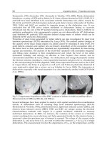
temperature (LNT) is presented in Fig. 2.2. Comparison of time resolved bands shows
clearly the increase of the initial CL intensity of the emission bands as the specimen
temperature is reduced to LNT may be because of the reduction in the thermally assisted
conversion of STE's to complementary defect pairs (oxygen deficient centers and oxygen
excess centers) via nonradiative relaxation processes [Stevens-Kalceff 1998].
In Fig. 2.2 the amplitudes of the main luminescence peaks: red, R (650 nm, 1.85 eV), blue,
B (460 nm, 2.7 eV), and UV (290 nm, 4.4 eV) have been recorded as a function of the
irradiation time.
The UV band shows slightly increasing behavior for some 10 sec then stabilizing up to the
saturation state. Using "track-stop" techniques [Fitting et al. 2004] it was possible to describe
this band more comprehensively. The UV band is detected initially in the "track" mode
followed by an increase at the beginning of the "stop" measurement, then a maximum
(turnaround), decreasing and increasing again to a long term invariance, larger for the wet
oxide than for the dry one.
The B band has a time dependence at LNT that differs from that at RT. Whereas it decreases
at LNT for both the wet and the dry SiO
2
, it increases from very low intensity for RT, i.e. it is
fully generated during the irradiation process, probably from precursors like ODC centers
[Fitting et al. 2002b]. The long term irradiation shows an increase to saturation even over
several hours. The Y band has the same time dependence as the B band both at RT and LNT.
It gives us an impression that both defect centers associated with the blue and the yellow
luminescence are at least of the same kind, probably oxygen deficiency centers (ODC).
The most obvious difference in the luminescence of wet and dry oxides appears in the R
dose dependence, Fig. 2.2 (top). Whereas the R luminescence of the wet oxide starts from an
initial intensity, decreases to a minimum and then increases to a saturation, the red band
dependence of the dry oxide differs: starting from a much lower intensity, increasing and
approaching nearly the same saturation intensity as that of wet oxide. This is the main new
finding for the different wet and dry oxides and therefore it will be discussed in more detail
in dependence of other ion implantations, especially hydrogen which is the main key
difference between the dry and wet oxide silicas. The red (≈1.9 eV) luminescence is generally
associated with NBOHC and attributed to the recombination of electrons in the highly
localized nonbridging oxygen band gap state, with holes in the valence-band edge [Stevens-
Kalceff 1998]. A remarkable difference in the dose behavior of the red peak in dry and wet
specimens is found. This can be considered as a well recognized proof that the NBOHC
Silicon Nanocluster in Silicon Dioxide: Cathodoluminescence,
Energy Dispersive X-Ray Analysis and Infrared Spectroscopy Studies
177
defect structure of SiO
2
is extremely sensitive to hydrogen treatment which can result in the
formation of defects and/or the formation of existing defect precursors in the presence of
hydrogen atoms [Fitting et al. 2005a]. Other methods than CL have provided direct/indirect
evidence for the existence of a number of different defect precursors for the NBOHC.
Based on these facts, we may express two interactions where NBOHCs are involved;
Dry SiO
2
: ≡Si−O···Si≡→ ≡Si−O● + ●Si≡ (2.1)
Wet SiO
2
: ≡Si−O● + H
o
↔ ≡Si−O−H (2.2)
0
100
200
300
400
500
600
CL-intensity (a.u.)
R: 650 nm
a
wet SiO : = 250 nm
dry SiO : = 200 nm
2
ox
2
ox
d
d
R: 650 nm
a
0
100
200
300
400
500
600
CL-intensity (a.u.)
Y: 575 nm
a
wet SiO : = 250 nm
dry SiO : = 200 nm
2
ox
2
ox
d
d
Y: 575 nm
a
0
100
200
300
400
500
600
CL-intensity (a.u.)
B: 465 nm
a
wet SiO : = 250 nm
dry SiO : = 200 nm
2
ox
2
ox
d
d
B: 465 nm
a
1 10 100 1000 10000
0
100
200
300
400
500
600
irradiation time (sec)
CL-intensity (a.u.)
UV: 290 nm
a
wet SiO : = 250 nm
dry SiO : = 200 nm
2
ox
2
ox
d
d
UV: 290 nm
a
Y: 575 nm
a
wet SiO : = 250 nm
dry SiO : = 200 nm
2
ox
2
ox
d
d
Y: 575 nm
a
B: 465 nm
a
wet SiO : = 250 nm
dry SiO : = 200 nm
2
ox
2
ox
d
d
B: 465 nm
a
UV: 290 nm
a
wet SiO : = 250 nm
dry SiO : = 200 nm
2
ox
2
ox
d
d
UV: 290 nm
a
R: 665 nm
a
wet SiO : = 250 nm
dry SiO : = 200 nm
2
ox
2
ox
d
d
R: 665 nm
a
1 10 100 1000 10000
irradiation time (sec)
at room temperature ( RT)at room temperature ( RT) at liquid nitrogen temperature ( LNT)at liquid nitrogen temperature ( LNT)
0
100
200
300
400
500
600
0
100
200
300
400
500
600
0
100
200
300
400
500
600
1
0
100
200
300
400
500
600
Fig. 2.2 CL dose dependencies of the red (R), the blue (B), the yellow (Y) and the ultraviolet
(UV) bands in dry and wet SiO2 at room temperature (RT) and liquid nitrogen temperature
(LNT); electron beam energy E
o
=10 keV: current density j
o
=5.4 mA/cm
2
.
Crystalline Silicon – Properties and Uses
178
The most common production mode for the NBOHC in dry SiO
2
which contains a negligible
amount of hydrogen and silanol groups, is by the strained bonds "···" between Si and O
atoms, eq. (2.1), here both the E´-center and NBOHC can form in dry oxide layers. In wet
SiO
2
, hydrogen diffuses through the network and simultaneously undergoes reactions with
the NBOHC during the first seconds of irradiation (destructive mode of NBOHC) followed
by a slow creation mode [Tandon 2004]. This decay process is attributable to the
simultaneous recombination of NBOHC with dissociated hydrogenous species, eq. (2.2). In
wet SiO
2
layers, NBHOC are likely to react with interstitial molecular hydrogen at room
temperature according to eq. (2.3).
≡Si−O● + H
2
→ ≡Si−O−H + H
o
(2.3)
Both of these reactions of eqs. (2.2) and (2.3) reasonably explain the elimination of NBOHC
in wet layers. Indeed, infrared (IR) measurements confirm that H
o
or H
2
react with dangling
bonds created by neutron irradiation [Bakos et al. 2004a]. But the most interesting point is
that the formation and destruction mechanism of NBOHC has absolutely no dependence on
a specimen's temperature because it is affected only by OH groups or hydrogen
concentration, as is clearly shown with the red curves in Fig. 2.2.
In the dry SiO
2
, the NBOHC defect concentration has the tendency to increase (creation) at
both RT and LNT during the beginning of irradiation but it decreases in wet specimens
(hydrogenated) due to interaction with the mobile hydrogen [Kajihara et al. 2002]. The
intensity difference of NBOHC between the beginning and the end of electron irradiation is
much less in wet SiO
2
, which confirms the reliability of eqs. (2.1-2.3).
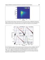
2.3 Lifetime measurement of the resolved CL bands
To identify whether the red bands in wet and dry oxide are due to the same electronic state
we have measured their respective lifetimes. In Fig. 2.3 the pulsed luminescence of the red
peak R (650 nm, 1.9 eV) is measured, and the red R luminescence decay with its lifetime, τ, is
determined from the pulse switching-off decay (bottom). In the pulsed CL response we
observe an increase and pumping of the luminescence over about 20 μs after switching on
the electron beam. The overall pulse duration is 100 μs.
During this excitation the luminescence again decays very rapidly over about 30 μs to lower
intensity. Of course, the first suggestion for such a change could be based on thermal
quenching effects of the red luminescence due to electron beam heating of the irradiation
spot on the sample. Indeed, the electron beam density with 0.1 A/cm
2
is about 20 times
higher than that in the CL dose measurements in Figs. 2.1 and 2.2. However, this very rapid
rise, turnaround, and decrease of the red luminescence at the beginning of the electron beam
pulse may be discussed also in the context of Fig. 2.2 and in terms of center activation and
destruction.
The red luminescence lifetime after switching-off the electron beam has been enlarged in the
bottom of Fig. 2.3 showing a mean lifetime of about (4.7±0.2) μs for the wet oxide and
(5.3±0.2) μs for the dry silicon dioxide layers, respectively. Thus we may state that the R
luminescence lifetime in wet oxide is somewhat smaller than in dry oxide, but of the same
order with τ~5 μs. However, the time dependence of the decay is not exponential, but a
stretched exponential with (5≤τ≤20μs over longer decay ranges [Trukhin et al. 2003a]. The
lifetime of the blue luminescence is measured too, in Fig. 2.4 the B band decay is indicating a
rapid component with τ≈(50±8) μs as well as a slow one with τ≈(7.1±0.4) ms for the wet
Silicon Nanocluster in Silicon Dioxide: Cathodoluminescence,
Energy Dispersive X-Ray Analysis and Infrared Spectroscopy Studies
179
oxide, and τ≈(70±2) μs as well as a slow one with τ≈(7.8±0.8) ms for the dry oxide.
Ultimately, the decay kinetics of the UV luminescence was measured by Goldberg
[Goldberg 1996] at LNT and RT. The decaying process was found to be occurring over the
first 5 ns followed by a hyperbolic one proportion to t
-1.5
in the μs range.
0 50 100 150 200
0
50
100
150
200
CL-amplitude (a.u.)
time ( s)m
0 50 100 150 200
time ( s)m
120 125 130 135 140 145
0
20
40
60
80
decay time ( s)m
120 125 130 135 140 145
decay time ( s)m
a
on
a
on
a
pulse
a
pulse
a
off
a
off
a
on
a
on
a
pulse
a
pulse
a
off
a
off
a
off
a
off
a
off
a
off
wet SiO
2
R: 650 nm, 1.9 eV
wet SiO
2
R:
650 nm, 1.9 eV
wet SiO
2
R: 650 nm, 1.9 eV
wet SiO
2
R:
650 nm, 1.9 eV
dry SiO
2
R: 650 nm, 1.9 eV
dry SiO
2
R:
650 nm, 1.9 eV
dry SiO
2
R: 650 nm, 1.9 eV
dry SiO
2
R:
650 nm, 1.9 eV
CL-amplitude (a.u.)
a
t.
(4.7 0.2) sm
K
a
t.
(5.3 0.2) sm
K
0
50
100
150
200
CL-amplitude (a.u.)
0
20
40
60
80
CL-amplitude (a.u.)
Fig. 2.3 CL pulsed excitation of the red R luminescence: 650 nm, 1.9 eV (top) with its
temporary decay and lifetime τ (below) for wet (left) and dry (right) SiO
2
at RT; electron
beam energy E
o
=5 keV: current density j
o
= 0.1 A/cm
2
, [Fitting et al. 2005b].
0
50
100
150
200
0 50 100 150 200
CL-amplitude (a.u.)
time ( s)m
a
on
a
on
a
pulse
a
pulse
a
off
a
off
wet SiO
2
B: 465 nm, 2.7 eV
wet SiO
2
B:
465 nm, 2.7 eV
CL-amplitude (a.u.)
0
200
400
600
800
0 50 100 150 200
time ( s)m
dry SiO
2
B: 465 nm, 2.7 eV
dry SiO
2
B:
465 nm, 2.7 eV
a
on
a
on
a
pulse
a
pulse
a
off
a
off
a
t
2
.
(7.8 0.8) ms
a
t
1
.
(70 2) sm
K
K
a
t
2
.
(7.1 0.4) ms
a
t
1
.
(50 8) sm
K
K
Fig. 2.4 CL pulsed excitation of the blue B luminescence: 465 nm, 2.7 eV with its temporary
decay and lifetime τ for wet and dry SiO
2
at RT; E
o
=5 keV: j
o
= 0.1 A/cm
2
.
2.4 Under-stoichiometric silica layers
The presence of intrinsic defects like oxygen vacancies or a presence of hydrogen atoms,
plays an important role in numerous circumstances particularly in the growth of the layer
structure. Thermal-annealing procedure leads to elimination of hydrogen and production of
silicon nanoclusters in different sizes in silica network depending on the applied
temperature. At annealing temperatures even below 900 °C, the hydrogen release from the
Crystalline Silicon – Properties and Uses
180
SiO
x
layers permits the formation of Si-O● radicals introducing structural disorder into the
layer network [Fitting et al. 2005a]. At higher temperatures, the structure will undergo a
network reaction similar to eq. (2.4), then giving rise to the formation of nanostructures.
SiOx → (x/2) SiO
2
+ (1-x/2)Si 1≤x≤2 (2.4)
In many cases cluster formation is affected by various kinds of defects in the Si-O network,
which can be either crystalline or amorphous. Fourier transform infrared spectroscopy
(FTIR) [Zacharias et al. 2003] and Cathodoluminescence (CL) [Fitting et al. 2002b] has been
employed to characterize the silicon cluster growing and to study the effects of ionizing
radiation on the structure of luminescent defects in SiO
x
systems [Trukhin and Fitting 1999,
Trukhin et al. 1999]. The UV (4.3 eV), the blue (2.7 eV) and the red (1.9 eV) luminescence
centers have been classified as process-induced centers, which also exist in irradiated SiO
2
.
Again the yellow luminescence band (2.15 eV) is distinguished more clearly in the SiO
x
layer, which we think deserves more attention and has to be studied intensively. In the
present section, the annealing temperature dependence of the CL intensities of the 4.3, 2.7,
2.15 and 1.9 eV peaks and their correlation with the stoichiometry x will be demonstrated
separately in order to associate the luminescence bands with the nature of different defects.
2.5 Fourier transform Infrared (FTIR) measurement of stoichiometric and under-
stoichiometric silica layers
The vibrational spectrum of SiO
2
is full of details. It consists of longitudinal-optical (LO) and
transversal-optical (TO) split features at around 460 cm
-1
, 800 cm
-1
, and 1100 cm
-1
. The LO
modes are not detected (lower frequencies) or only detected in oblique incidence IR
transmission measurements. The highest frequency feature exhibits the largest absorption
coefficient, therefore in the literature most attention is paid to this absorption band. In SiO
2
it
features a TO absorption peak at around 1090 cm
-1
with a LO absorption at around 1250cm
-1
,
being visible when applying oblique incident IR radiation. In the present work we focus on
the region of the Si−O−Si stretching mode (700-1400 cm
-1
).
500 1000 1500 2000 2500 3000 3500 4000
0
50
100
150
wavenumber (cm )
-1
transmittance %
dry
SiO
2
dry
SiO
2
wet
SiO
2
wet
SiO
2
700 800 900 1000 1100 1200 1300 1400
0
20
40
60
80
100
wavenumber (cm )
-1
transmittance %
Fig. 2.5 Fourier transform infrared (FTIR) spectra of thermally grown pure dry and wet SiO
2
.
Silicon Nanocluster in Silicon Dioxide: Cathodoluminescence,
Energy Dispersive X-Ray Analysis and Infrared Spectroscopy Studies
181
without
excess oxygen
43 %
without
excess oxygen
42 %
30
20
10
0
40
50
60
70
80
90
100
IR transmittance (%)
700 800 900 1000 1100 1200 1300 1400
wavenumber (cm )
-1
700 800 900 1000 1100 1200 1300 1400
wavenumber (cm )
-1
-SiOa
2
-SiOa
2
7x10 mbar
O pressure
-4
2
5x10
-4
1x10
-4
5x10
-5
1x10
-5
-SiOa
1
-SiOa
1
-SiOa
2
-SiOa
2
7x10
O pressure
-4
mbar
2
5x10
-4
1x10
-4
5x10
-5
1x10
-5
-SiOa
1
-SiOa
1
x 0.2 x 0.2
10921006810 10921034810 880
T
a
=1100 C
o
T
a
=1100 C
o
non-annealed
annealed
Fig. 2.6 Infrared spectra of SiO
x
layers on Si substrate grown by thermal evaporation of SiO
in ambient oxygen pressures, the stoichiometric SiO
1
and SiO
2
layers are presented for
calibration of non-annealed samples (left) and thermally annealed samples, T
a
=1100 °C
(right).
At first we present the IR spectra of thermally grown a-SiO
2
in Fig. 2.5, then a comparison of
the non-annealed and the thermally annealed (T
a
=1100 °C) silica layers with different
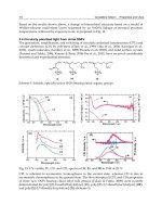
stoichiometry x, before they have been irradiated (Fig. 2.6).
Typical IR transmittance spectra of wet and dry silica are presented in Fig. 2.5. Obviously
there are no essential differences in spectra of silica samples with different thermal
oxidization method (wet or dry). The only bands observed are due to the fundamental SiO
2
vibrational bands. The oxygen to silicon ratio of several SiO
x
thin layers deposited by
thermal evaporation of silicon monoxide SiO and simultaneous oxidation are studied by
FTIR spectroscopy in order to determine the stoichiometric degree x.
The infrared properties of the non-annealed and annealed samples at 1100 °C are presented
in Fig. 2.6. Various silicon-oxygen related absorption bands can be identified in the wave
number region from 700 to 1400 cm
-1
. Due to the fact that the samples are produced under
such conditions that they are totally hydrogen-free we can exclude all hydrogen related IR
modes. The band around 810 cm
-1
is attributed to Si−O textendash Si bond bending motion
in SiO
2
[Tsu et al. 1989, Gucsik et al. 2004]. This band position increases when the sample
composition approaches the pure stoichiometric silica (SiO
2
) structure, while it is not
detectable in the sample produced without excess oxygen exposure. The most intense
feature in the spectra of Fig. 2.6 appears in the range of 1000-1100 cm
-1
, which is ascribed to
the Si−O−Si stretching vibrations [Lehmann et al. 1984]. The Si−O vibration frequency in
thermally annealed samples shifts from 1034 cm
-1
in the sample without excess of oxygen to
higher frequencies at 1092 cm
-1
in the sample of stoichiometric SiO
2
composition. The
transversal-optical (TO) peak positions have been determined by the zero-transition of the
Crystalline Silicon – Properties and Uses
182
first derivative. The increase in wavenumber is due to the fact that the number of Si−Si
bonds within the tetrahedral units decreases with the concomitant increase of Si−O bonds.
The same fact can explain the creation and the frequency shift of the 810 cm
-1
bending band.
These peak positions can be used for a basic estimation of the stoichiometry of
homogeneous SiO
x
structures and as a measure for the phase transition from SiO
1
to higher
x compositions SiO
x
up to SiO
2
.
In Fig. 2.7 we show the calibration of the stoichiometry degree x in SiO
x
layers as a function
of the Si−O−Si TO stretching mode frequency. We should mention that the position of the
TO stretching mode as a function of the stoichiometric degree x is always expressed as a
linear regressions-type formula, see e.g. [Tsu et al. 1989, Lehmann et al. 1984]. Different peak
position determination methods could be the reason for the discrepancy between our data
and those presented in the literature where mostly symmetric axis band positions have been
used previously. Here we consider the zero transition of the first derivative to obtain the
absolute peak position. Earlier a numerous equation in dependence on x was obtained
[Lehmann et al. 1984]:
ν
x
=(48.8x+976) cm
-1
(2.5)
The estimated x values in a linear relation according to Lehmann [Lehmann et al. 1984] are
shown as the dashed line in Fig. 2.7. Based on our IR data of the two well-calibrated and
fixed SiO
1
and SiO
2
layers we had to slightly modify the Lehmann relation and have
obtained the following approach for the growth of x in SiO
x
from nearly x>1 up to
stoichiometric SiO
2
:
ν
x
=(58x+976) cm
-1
(2.6)
960 980 1000 1020 1040 1060 1080 1100
0.0
0.5
1.0
1.5
2.0
2.5
n
TO
( ) = 58 +976
xx
wavenumber (cm )n
TO
-1
SiO
1
SiO
1
SiO
2
SiO
2
n
TO
( ) = 48.8 +987
xx
SiO non-annealed
x
SiO non-annealed
x
SiO annealed : =1100 C
x
a
T
o
SiO annealed :=1100C
x
a
T
o
x =1.97
in SiO
x
x
SiO :Si annealed
2
SiO :Si annealed
2
Fig. 2.7 Calibration of stoichiometry degree
x
in SiO
x
layers with the TO stretching mode
of IR measurements; dashed line: according to [Lehmann et al. 1984]; solid line: given by
the present SiO
1
and SiO
2
data of known stoichiometry, the wavenumbers of the annealed
SiO
x
samples were placed on this line; ∆ SiO
2
:Si ion-implanted sample from [Fitting et
al. 2002b].
This relation is presented in Fig. 2.7 as a solid line for the thermally annealed samples,
where x=1 and x=2 are given as fixed points and the other data were placed on this straight
line between SiO
1
and SiO
2
in order to determine their x. Of course, the non-annealed
samples will not fit to this straight line because their atomic network is still much more
Silicon Nanocluster in Silicon Dioxide: Cathodoluminescence,
Energy Dispersive X-Ray Analysis and Infrared Spectroscopy Studies
183
disordered than for the thermally annealed samples leading to higher TO mode softening,
see Figs. 2.5 - 2.7. Additionally, a Si
+
ion-implanted sample SiO
2
:Si with an Si excess of 4 at.%
in the maximum of the implantation profile has been investigated previously, providing a
mean stoichiometric degree over the full silica layer [Fitting et al. 2002b]. This value is close
to x=2 but there is already a remarkable shift of -∆ν
TO
=10 cm
-1
as can be seen in Fig. 2.7,
supporting the sensitivity of the IR measurement.
0.0
0.5
1.0
1.5
2.0
2.5
in SiO
x
x
10
-7
10
-6
10
-5
10
-4
10
-3
O ambient pressure (mbar)
2
10
-2
10
-1
SiO
1
SiO
1
Fig. 2.8 Stoichiometry x of SiO
x
layers as grown by thermal evaporation of SiO in oxygen
ambient pressure, based on FTIR measurements after thermal annealing of the samples.
Then in Fig. 2.8 the x values obtained by FTIR are correlated with the ambient oxygen
pressure during the evaporation of SiO
1
. So the stoichiometric transition from SiO
1
to SiO
2
as
a function of the ambient oxygen pressure can be estimated. An extrapolation shows that
SiO
2
layers can be manufactured roughly at oxygen pressure nearly to 1×10
-1
mbar.
2.6 CL of under-stoichiometric silica layers
In order to characterize the SiO
x
layers by their optical luminescence features,
cathodoluminescence (CL) studies of the SiO
x
samples were carried out at both room
temperature (RT) and liquid nitrogen temperature (LNT). see Fig. 2.9. This experiment was
performed using samples that were thermally annealed at T
a
=600, 800, 1100, 1300 °C besides
the normal non-annealed samples, this way we could follow the structure change/growing
under the influence of temperature treatment and the electron beam irradiation. Here we
used also the experimental parameters as described before in the previous sections.
Samples with x<1.3 show almost no CL signals and samples with x≈1.3 show quite weak
and smoothed CL intensities even when they annealed at high temperatures or cold down
to LNT. Thus, if the atomic ratio of silicon atoms is high compared with the ratio of oxygen,
i.e. x<1.3, the samples do not exhibit any characteristic CL, indicating deficiency of Si−O
bonds to form ordinary silica structures and any prominent silica defects.
Upon reaching x>1.5 , the CL intensities grow considerably but almost only the yellow
luminescence Y at 2.15 eV is detectable in the initial CL spectra (1 sec). After longer electron
beam irradiation (30 min) the characteristic silica bands UV, B, and R appear too, as can be
seen in Fig. 2.9.
Here the yellow Y luminescence band does not occur accidentally in hydrogen rich silica
samples, there we have attributed a similar band to hydrogen molecules on interstitial sites
in the silica network [Fitting et al. 2005a, Fitting et al. 2005b]. In Fig. 2.9 we see that the CL
Crystalline Silicon – Properties and Uses
184
SiO (Vt14)
=174 nm
1.29
d
ox
SiO (Vt14)
=174
nm
1.29
d
ox
CL-intensity (a.u.)
UV
B
Y
R
1 sec
30 min
| ||| | | | | | ||| | | || | | | | | | | | | | | | | |
UV
B
Y
R
1 sec
| ||| | | | | | ||| | | || | | | | | | | | | | | | | |
UV
B
Y
R
1 sec
30 min
UV
B
Y
R
1 sec
30 min
| ||| | | | | | ||| | | || | | | | | | | | | | | | | |
UV
B
Y
R
1 sec
30 min
||||| ||| | ||||||| | | | | | | | | | | | | | | |||| | ||| | ||| | | || | | | | | | | | | | | | | |
B
Y
R
1 sec
30 min
SiO
=300 nm
1
d
ox
SiO
=300
nm
1
d
ox
||||| ||| | ||||||| | | | | | | | | | | | | | |
0
5
10
15
UV
SiO
=300 nm
1
d
ox
SiO
=300
nm
1
d
ox
CL-intensity (a.u.)
B
Y
R
1 sec
| ||| | | | | | ||| | | || | | | | | | | | | | | | | | | ||| | | | | | ||| | | || | | | | | | | | | | | | | |
UV
B
Y
R
1 sec
30 min
SiO (Vt10)
=164 nm
0.84
d
ox
SiO (Vt10)
=164
nm
0.84
d
ox
| ||| | | | | | ||| | | || | | | | | | | | | | | | | |
0
5
10
15
CL-intensity (a.u.)
non-annealed - RTnon-annealed - RT
T
a
=600 C
o
T
a
=600 C
o
non-annealed - LNTnon-annealed - LNT
T
a
=800 C
o
T
a
=800 C
o
T
a
=1100 C
o
T
a
=1100 C
o
energy (eV)
6 5 4 3 2.5 2 1.8 1.6
T
a
=1300 C
o
T
a
=1300 C
o
energy (eV)
6 5 4 3 2.5 2 1.8 1.6
energy (eV)
6 5 4 3 2.5 2 1.8 1.6
energy (eV)
6 5 4 3 2.5 2 1.8 1.6
energy (eV)
6 5 4 3 2.5 2 1.8 1.6
energy (eV)
6 5 4 3 2.5 2 1.8 1.6
0
5
10
15
0
5
10
15
CL-intensity (a.u.)
CL-intensity (a.u.)
CL-intensity (a.u.)
CL-intensity (a.u.)
UV
B
Y
R
1 sec
30 min
| ||| | | | | | ||| | | || | | | | | | | | | | | | | |
SiO (Vt10)
=164 nm
0.84
d
ox
SiO (Vt10)
=164
nm
0.84
d
ox
30 min
30 min
UV UV
B
Y
R
1 sec
30 min
| ||| | | | | | ||| | | || | | | | | | | | | | | | | |
UV
B
Y
R
1 sec
30 min
UV
B
Y
R
1 sec
30 min
| ||| | | | | | ||| | | || | | | | | | | | | | | | | |
UV
B
Y
R
1 sec
30 min
SiO (Vt12)
=164 nm
1.12
d
ox
SiO (Vt12)
=164
nm
1.12
d
ox
| ||| | | | | | ||| | | || | | | | | | | | | | | | | |
CL-intensity (a.u.)
0
5
10
15
UV
B
Y
R
1 sec
30 min
| ||| | | | | | ||| | | || | | | | | | | | | | | | | |
SiO (Vt12)
=164 nm
1.12
d
ox
SiO (Vt12)
=164
nm
1.12
d
ox
0
5
10
15
UV
B
Y
R
1 sec
30 min
| ||| | | | | | ||| | | || | | | | | | | | | | | | | |
UV
B
Y
R
1 sec
30 min
| ||| | | | | | ||| | | || | | | | | | | | | | | | | |
UV
B
Y
R
1 sec
30 min
| ||| | | | | | ||| | | || | | | | | | | | | | | | | |
UV
B
Y
R
1 sec
30 min
| ||| | | | | | ||| | | || | | | | | | | | | | | | | |
UV
Y
30 min
| ||| | | | | | ||| | | || | | | | | | | | | | | | | |
10
20
30
40
R
B
1 sec
0
SiO (Vt14)
=174 nm
1.29
d
ox
SiO (Vt14)
=174
nm
1.29
d
ox
UV
B
Y
R
1 sec
30 min
| ||| | | | | | ||| | | || | | | | | | | | | | | | | |
| ||| | | | | | ||| | | || | | | | | | | | | | | | | |
Y
R
1 sec
30 min
UV
B
UV
B
Y
R
1 sec
30 min
UV
B
Y
R
1 sec
30 min
UV
B
Y
R
1 sec
30 min
| ||| | | | | | ||| | | || | | | | | | | | | | | | | |
| ||| | | | | | ||| | | || | | | | | | | | | | | | | |
| ||| | | | | | ||| | | || | | | | | | | | | | | | | |
UV
B
Y
R
1 sec
30 min
| ||| | | | | | ||| | | || | | | | | | | | | | | | | |
UV
B
Y
R
1 sec
30 min
| ||| | | | | | ||| | | || | | | | | | | | | | | | | |
G
UV
B
Y
R
1 sec
30 min
G
UV
B
Y
R
1 sec
30 min
G
UV
B
Y
R
1 sec
30 min
| ||| | | | | | ||| | | || | | | | | | | | | | | | | |
| ||| | | | | | ||| | | || | | | | | | | | | | | | | |
| ||| | | | | | ||| | | || | | | | | | | | | | | | | |
G
B
Y
R
SiO (Vt18)
=174 nm
1.53
d
ox
SiO (Vt18)
=174
nm
1.53
d
ox
0
50
100
| ||| | | | | | ||| | | || | | | | | | | | | | | | | |
UV
B
Y
R
1 sec
30 min
| ||| | | | | | ||| | | || | | | | | | | | | | | | | |
G
UV
B
Y
R
1 sec
30 min
| ||| | | | | | ||| | | || | | | | | | | | | | | | | |
G
UV
B
Y
R
1 sec
30 min
G
UV
B
Y
R
1 sec
30 min
G
UV
B
Y
R
1 sec
30 min
| ||| | | | | | ||| | | || | | | | | | | | | | | | | |
| ||| | | | | | ||| | | || | | | | | | | | | | | | | |
| ||| | | | | | ||| | | || | | | | | | | | | | | | | |
UV
B
Y
R
1 sec
30 min
| ||| | | | | | ||| | | || | | | | | | | | | | | | | |
G
G
UV
B
Y
R
1 sec
30 min
| ||| | | | | | ||| | | || | | | | | | | | | | | | | |
G
UV
B
Y
R
1 sec
30 min
G
UV
B
Y
R
1 sec
30 min
G
UV
B
Y
R
1 sec
30 min
| ||| | | | | | ||| | | || | | | | | | | | | | | | | |
| ||| | | | | | ||| | | || | | | | | | | | | | | | | |
| ||| | | | | | ||| | | || | | | | | | | | | | | | | |
UV
B
Y
R
1 sec
30 min
| ||| | | | | | ||| | | || | | | | | | | | | | | | | |
SiO
=200 nm
2
d
ox
SiO
=200
nm
2
d
ox
G
UV
B
Y
R
1 sec
30 min
| ||| | | | | | ||| | | || | | | | | | | | | | | | | |
| ||| | | | | | ||| | | || | | | | | | | | | | | | | |
UV
B
Y
R
1 sec
30 min
UV
B
Y
R
1 sec
30 min
UV
B
Y
R
1 sec
30 min
| ||| | | | | | ||| | | || | | | | | | | | | | | | | |
| ||| | | | | | ||| | | || | | | | | | | | | | | | | |
| ||| | | | | | ||| | | || | | | | | | | | | | | | | |
UV
Y
1 sec
30 min
SiO (Vt16)
=174 nm
1.34
d
ox
SiO (Vt16)
=174
nm
1.34
d
ox
| ||| | | | | | ||| | | || | | | | | | | | | | | | | |
0
10
20
30
0
20
40
60
80
100
UV
B
Y
R
1 sec
30 min
SiO (Vt19)
=174 nm
1.55
d
ox
SiO (Vt19)
=174
nm
1.55
d
ox
| ||| | | | | | ||| | | || | | | | | | | | | | | | | |
30 min
1 sec
40
0
50
100
0
20
40
60
80
100
0
50
100
150
200
250
0
10
20
30
40
R
B
Y
R
1 sec
30 min
UV
B
0
200
400
600
800
SiO (Vt16)
=174 nm
1.34
d
ox
SiO (Vt16)
=174
nm
1.34
d
ox
SiO (Vt18)
=174 nm
1.53
d
ox
SiO (Vt18)
=174
nm
1.53
d
ox
SiO (Vt19)
=174 nm
1.55
d
ox
SiO (Vt19)
=174
nm
1.55
d
ox
SiO
=200 nm
2
d
ox
SiO
=200
nm
2
d
ox
CL-intensity (a.u.)
CL-intensity (a.u.)
CL-intensity (a.u.)
CL-intensity (a.u.)
200 300 400 500 600 700 800
wavelength (nm)
200 300 400 500 600 700 800
wavelength (nm)
200 300 400 500 600 700 800
wavelength (nm)
200 300 400 500 600 700 800
wavelength (nm)
200 300 400 500 600 700 800
wavelength (nm)
200 300 400 500 600 700 800
wavelength (nm)
CL-intensity (a.u.)
CL-intensity (a.u.)
CL-intensity (a.u.)
CL-intensity (a.u.)
UV
0
10
20
30
40
Fig. 2.9 CL spectra of SiO
x
layers with thickness d
ox
grown on Si substrate with different
ambient oxygen pressure and having been thermally annealed at different temperatures T
a
.
The initial and the saturated CL spectra are labeled by "1sec" and "30 min", respectively.
Silicon Nanocluster in Silicon Dioxide: Cathodoluminescence,
Energy Dispersive X-Ray Analysis and Infrared Spectroscopy Studies
185
NBOHC
O
Si
O
O
Si
O
O
Si
O
O
Si
O
Si
O
Si
O
O
O
Si
O
ODC
O
Si
O
Si
O
O
O
Si
O
O
O
O
NBOHC
O
O
Si
O
O
Si
O
Si
O
O
O
Si
O
O
O
6 folded silicon ring
O
O
Si
O
<T
a
1100 C
o
e
-
>T
a
1100 C
o
e
-
ODC as Si dimer Si trimer Si hexamer ring
O
O
Si
O
Fig. 2.10 Schematic presentation of the nonbridging oxygen hole center (NBOHC) and
oxygen deficiency center (ODC) forming a Si dimer in the SiO
2
network (left) transformed
by thermal annealing at temperatures T
a
and/or electron beam irradiation to Si trimers
(middle) and further on to elementary 6-fold silicon rings (Si hexamers) as a first step of Si
nanocrystal formation (right).
spectra of dry and under-stoichiometric SiO
x
layers (both are H-free), annealed up to
relatively high temperatures in vacuum show a very intense yellow luminescent band at
2.15 eV. After annealing to temperatures T
a
>1100 °C the Y luminescence is detectable too,
even with higher intensity, which means it is increasing with T
a
. We may conclude that the
silicon atoms tend to re-arrange themselves in small clusters as chains or rings in the SiO
x
network [Nicklaw et al. 2000], and that could be one of the most dominant origins for the Y
luminescence in dry silica. In the absence of water there are strained bonds or defects of the
form ≡Si−O···Si≡, where O···Si represents a strained (weak) Si−O bond that could be
transformed into small membered silicon rings (3, 4-membered) [Ivanda et al. 2003] as well
as to nonbridging oxygen hole centers (NBOHC) as an effect of high temperature treatment,
as illustrated in Fig. 2.10.
A careful temporal observation of Fig. 2.10 makes it clearer that the cluster can be separated
into core and surface components. The core is nucleation of silicon atoms (silicon bonded
together) but on the surface both silicon and oxygen have dangling bonds, with the oxygen
atom tending toward the surface. These fragments residing on the surface tend to be highly
mobile [Schweigert et al. 2002], so we may state that the yellow luminescence is exciting
from the surface of the silicon nanoclusters and not from the silicon core.
The red R (1.9 eV) emission is generally associated with the NBOHC and attributed to the
recombination of electrons in the highly localized nonbridging oxygen band gap state
with holes in the valence-band edge [Stevens Kalceff 1998]. On the other hand, tempering
to T
a
≈1300 °C leads to a further increase of the yellow band Y and to a strong reduction of
the red band R. Probably, at these high temperatures oxygen is released from the SiO
x
network diminishing the red luminescence but forming more oxygen deficient centers
ODC and Si-rings.
In other words, more oxygen dangling bonds and oxygen deficient centers can be created
due to high temperature exposure. Then silicon fragments or rings are produced in the silica
network which seems to be the most probable candidates for the yellow Y luminescence
center in silica.
2.7 EDX, CL and TEM investigation of Si cluster formation in modified silica
The formation of oxygen deficient centers (ODC) or even higher silicon aggregates by means
of electron beam irradiation has been manifested already earlier [Fitting et al. 2002b,
Trukhin et al. 1999, Fitting et al. 2005b, Stevens Kalceff 1998]. Even Auger electron
spectroscopy (AES) has clearly evidenced that oxygen is dissociated from SiO
2
due to
Crystalline Silicon – Properties and Uses
186
electronic or thermal processes during electron beam excitation, see e.g. [Stevens Kalceff
1998, Cazaux 1986]. Thus the blue B and the red R luminescence bands grow under electron
bombardment to a saturation after an irradiation dose of about 3 As/cm
2
[Fitting et al.
2002b], see the bottom row in Fig. 2.9.
In order to demonstrate the ODC increase during electron bombardment we have
determined the stoichiometric degree x of SiO
x
by means of energy-dispersive X-ray
analysis (EDX) during electron irradiation (E
o
=10 keV, j
o
=2 mA/cm
2
) in initially
stoichiometric silica layers SiO
2
. The results are presented in Fig. 2.11. There we see a
decrease of x with irradiation time, as expected, for room temperature (RT) faster than for
liquid nitrogen temperature (LNT). The initial values with x>2.04 are somewhat higher than
the expected ones x=2 of stoichiometric silica but we suppose an excess of oxygen on
interstitial sites within the silica network remaining still from the oxidation process and the
thermal diffusion of oxygen through SiO
2
towards the interface at the Si substrate. It is well
known that over-stoichiometric silica with x>2 does not exist [Helm and Deal 1993], besides
some peroxy bridges ≡Si−O−O−Si≡ or radicals as candidates or precursors for luminescent
defects [Pacchioni et al. 2000], however, in very low concentration. This interstitial excess
oxygen may form O
2
and O
-
2
molecules [Fitting et al. 2005c].
0 2000 4000 6000 8000 10000
1.90
1.92
1.94
1.96
1.98
2.00
2.02
2.04
2.06
2.08
2.10
EDX : = 10 keV
= 2 mA/cm
E
j
o
o
2
EDX :=10 keV
=
2 mA/cm
E
j
o
o
2
LNT
RT
irradiation time (sec)
in SiO
x
x
Fig. 2.11 EDX measurement of the oxygen to silicon ratio x in initially stoichiometric silica
layers SiO
2
during electron beam irradiation at room temperature (RT) and liquid nitrogen
temperature (LNT).
123456789101112
0
10
20
30
40
50
60
70
diameter (nm)
count per nm
20 nm20 nm
Fig. 2.12 TEM micrograph showing Si nanoclusters embedded in the silica matrix (left) and
the related cluster size distribution (right) of a 250 nm SiO
2
layer having been irradiated for
30 min by an electron beam of 5 keV and 2.7 A/cm
2
, [Salh et al. 2006].
Silicon Nanocluster in Silicon Dioxide: Cathodoluminescence,
Energy Dispersive X-Ray Analysis and Infrared Spectroscopy Studies
187
photon energy (eV)
1.0 1.2 1.4 1.81.6
CL-intensity (a.u.)
20
40
60
0
0
10
15
20
5
electron beam modified SiO
2
electron beam modified SiO
2
1.12 eV1.12
eV
1.16 eV1.16
eV
1.28 eV1.28
eV
1.58 eV1.58 eV
c-Sic - Si
Fig. 2.13 CL spectra of electron beam modified SiO
2
showing in the near IR the fundamental
transition of c-Si at hν=1.1 eV, of a-Si at 1.3 eV and a transition in Si nanocrystals (quantum
dots) at 1.6 eV.
In order to demonstrate the oxygen dissociation and the formation of ODC, and finally, of Si
clusters under electron bombardment we have carried out an additional experiment under
high dose electron irradiation. Therefore thin 250 nm-thick silica films have been prepared
by wet thermal oxidation on silicon wafers. Afterwards the silicon substrate had been
removed by mechanical milling and 3 keV Ar
+
ion etching. In this way self-supporting 250
nm thin silica films had been prepared for imaging in a transmission electron microscope
(TEM). More details of preparation are given in [Kolesnikova et al. 2005].
These films were modified by heavy electron beam irradiation: beam energy 5 keV, current
20 nA over an area of 3/4 μm
2
yielding a high current density of 2.7 A/cm
2
. Thus we may
assume electronic as well as thermal dissociation [Kolesnikova et al. 2005] of oxygen from
the thin SiO
2
layers and more and more the appearance of under-stoichiometric SiO
x
. This
SiO
x
will undergo a phase separation as described by eq.(2.4). After 30 minutes of electron
beam irradiation we observe Si cluster formation as presented in Fig. 2.12. The Si clusters
embedded in the silica appear as dark spots. Their size distribution is shown in the right
part of Fig. 2.12. There we see a most probable cluster diameter of 4 nm and a maximum
diameter of 10 nm. As it has already been shown in the context of formation of Ge
nanocrystallites in Ge-implanted silica, [Fitting et al. 2002b], such largely extended clusters
will diminish the Si-related luminescence. The right size for elementary small luminescent
clusters should be searched in intermediate regions, i.e. according to Fig. 2.10 between Si
dimers (ODC) and hexamer rings.
Fig. 2.13 shows the CL spectra of pure crystalline Si and the spectra of Si nanoclusters
embedded in the host silica. Luminescence bands are observed at around 1.1 eV and 1.3 eV
assigned to crystalline and amorphous silicon phases, respectively. Another band at 1.6 eV
is also to be seen after heavy electron beam bombardment in the SiO
2
structure. In spite of
extensive experimental and theoretical work during the last years, the light-emitting
mechanism which explains emission at 1.6 eV has not been fully understood yet. It is
believed that the oxygen-related light-emitting centers are positioned at the interface
between the Si nanoclusters and the host oxide [Prokes et al. 1998]. A broad CL emission
band is characteristic of Si nanoclusters. Although the spectra vary considerably in intensity
after longer irradiation, the peak position does not shift significantly, implying a similar
Crystalline Silicon – Properties and Uses
188
mean size for the nanocrystals. No unique relation between the CL or PL emission energies
and Si nanocluster sizes has been reported in the literature making the quantitative
comparison of the results difficult [Wilkinson and Elliman 2004]. Other authors estimated
that 5 nm Si nanoclusters emit at 1.6 eV, while 3 nm Si nanoclusters give PL at 2 eV [Ledoux
et al. 2002]. On the contrary it was reported that 4 nm Si nanoclusters emit at 1.3 eV and the
1.6 eV PL correspond to very small sizes of about 1 nm [Iacona et al. 2000].
PL-intensity (a.u.)
1.1 1.2 1.3 1.4 1.5 1.6 1.7 1.8
0.0
0.2
0.4
0.6
0.8
1.0
1.2
energy (eV)
diameter equal or below
3.8 nm 2.0 nm
diameter equal or below
3.8
nm 2.0 nm
1100 1000 900 800 700750850
energy (eV)
wavelength (nm)
Fig. 2.14 Normalized photoluminescence spectra showing a blue shift correlated with the Si
nanocrystal size, [Zacharias et al. 2002].
Recently Si nanocrystals have been fabricated by thermal treatment of SiO-SiO
2
nanolattices,
in a way which makes it possible to control not only the size but also the density and the
arrangements of the nanocrystals independently of the stoichiometry [Zacharias et al. 2002,
Yi et al. 2003, Torchynska 2006]. In this method a strong photoluminescence (PL) and a size
dependent shift of the PL position are shown as a proof of size control. A strong blue shift
from 960 nm (1.3 ev) to 810 nm (1.5 eV) with decreasing nanocrystal size was observed with
respective cluster sizes 3.8 nm and 2 nm, respectively, see Fig. 2.14.
3. Hydrogen implanted SiO
2
Direct hydrogen implantation or exposure of SiO
2
to water vapor results in the appearance of
various OH bands, for example water molecules are known to form silanol (Si−O−H) groups
in the oxide [Bakos et al. 2004b], but the relative concentration of silanol to interstitial water
depends on the way the oxide was manufactured and subsequently treated, raising questions
about the most stable form of water in the oxide and the role of hydrogen in this reaction.
Hydrogen plays an essential role in the thermal oxidation process, either through the
interaction with point defects or as interstitial atoms in the SiO
2
network. Hydrogen can be
considered as an important accidental impurity or an intentional additive in all forms of silicon
dioxide which can passivate dangling bonds and produce high-quality interfaces [Rashkeev et
al. 2001]. Besides, it can reduce electrical activity of point and extended defects by inducing
grain boundaries and it saturates oxygen dangling bonds (NBOHC ≡Si−O●) or the threefold-
coordinated SiO
2
defect (E´-center ≡Si●), through the chemical reactions:
≡Si−O● (or ≡Si●) +H
o
→ ≡Si−O−H (or Si−H) (3.1)