Photodiodes Communications Bio Sensings Measurements and High Energy Part 6 pptx
Bạn đang xem bản rút gọn của tài liệu. Xem và tải ngay bản đầy đủ của tài liệu tại đây (1.59 MB, 20 trang )
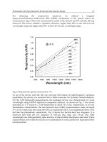
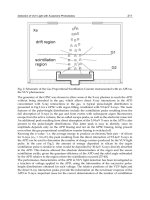
Low Scattering Photodiode-Modulated Probe For Microwave Near-Field Imaging 13
Z
ON
and Z
p
+ Z
OFF
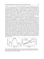
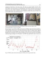
(see Fig.7). In fact, if a simple capacitor model is assumed for the short
dipole in free-space, resonance frequencies of 2.53 GHz and 3.09 GHz can be calculated for the
ON and OFF states respectively. Results from a simulation done with the thin-wire method
of moment are also shown in the figure. In the simulation, the probe is illuminated with a
uniform plane wave in free space. This shows the normalized difference between the squared
scattered field taken 1 cm away from the dipole in the two states. The results also exhibit
a double peak response. In the measurement, the resonance observed in the waveguide
are shifted to lower frequencies. This shift is thought to be due to imperfections in the
construction and uncertainty in the substrate’s constitutive material parameters. Furthermore,
the value of Z
p
in free-space is not the same as in the waveguide where the dipole is interacting
with the metallic walls. Finally, as these reflection differences are obtained by subtracting
very similar measured values, the results are susceptible to measurement and simulation
inaccuracies. Both curves exhibits a maximum sensitivity near the design frequency of 2.45
GHz. Finally, the waveguide measurement process described above was simulated in HFSS.
The reflection coefficient difference shown in Fig. 13 exhibits peaks near 2.7 GHz and 3 GHz. It
should be noted that this curve is derived from differences between S
11
values with a variation
smaller than 5
×10
−5
in magnitude. Therefore, the frequency shift compared to the other two
curves may be partly due to simulation inaccuracies.
Fig. 13. Difference of frequency response for the OMS probe in ON and OFF states: solid line
is the measured reflection coefficient; dashed line is the simulated scattered field; dotted line
is simulated reflection coefficient.
8. OMS probe performance validation
In order to verify the performance of the developed OMS probe, it was set to measure the
electric field distribution near a 50-Ω microstrip transmission line. The test was made in a
monostatic setup, where the measured signal is proportional to the square of the complex
electric field (v ∝ E
2
). The transmission line was fabricated on a Rogers substrate (RO3035)
with a relative permittivity of 3.8 and a thickness of 60 mils (Fig. 14).
The rapidly varying fields near the line are highly suitable to assess the resolution and the
dynamic range of the measurement system. In this measurement, the probe is scanned across
the microstrip line at a height of 3 mm above it, and measures the transverse electric field
91
Low Scattering Photodiode-Modulated Probe for Microwave Near-Field Imaging
14 Photodioes
distribution along x (i.e., E
x
) (Fig. 14). The transmission line was terminated with a matched
load.
To validate the measurement results, we also included the field distribution of the
transmission line predicted by HFSS (Fig. 15).The results obtained from simulation need to
be post-processed to take into account the effect the finite length of the measuring probe. This
topic will be discussed in Section 9.
Fig. 14. Schematic of the probe and microstrip transmission line under test.
(a) Magnitude (b) Phase
Fig. 15. Measurement results and simulations (magnitude and phase) of electric field (E
x
)at
h =3mm.
8.1 Taking the square root: sign ambiguity removal
When the NF imager operates in monostatic mode, the measured fields are obtained by taking
the square root of the measured data. The square root of a complex signal v
= X
I
+ jX
Q
has two solutions and it is necessary to select the proper one. The procedure might be
straightforward when the measured field takes nonzero values. In this case it is possible to
ensure continuity of the phase distribution in the whole data set. In contrast, sign retrieval is
not an easy task if nulls occur (i.e., E
= 0) at some locations. In these cases, no clear method
has been addressed to choose the sign of the square root correctly. However, a technique was
reported in (Hygate & Nye, 1990) for some particular cases.
In the case of the microstrip line considered here it is well known that transverse electric field
(E
x
in Fig. 14) has a null on the strip’s symmetry plane and a different sign on both sides.
Thus, even if choosing the sign of the electric field on either side is impossible without a priori
92
Photodiodes – Communications, Bio-Sensings, Measurements and High-Energy Physics
Low Scattering Photodiode-Modulated Probe For Microwave Near-Field Imaging 15
knowledge. It is assumed that when a contour with zero E field is crossed, the phase changes
by π.
9. Probe correction
The short dipole implementing the probe has a finite length. Therefore, the measured data is
not representative of the fields at a point but rather of the integral of the weighted field along
the probe. To take this effect into account, we used the induced e.m.f method for calculating
the induced voltage across the probe’s terminal generated by an incident E-field (see Fig. 16a).
In this method, we need to know the current distribution (J) on the probe when it is radiating,
i.e., acting as a transmitting antenna. Since the length of the probe is shorter than 0.1λ, one can
assume that J can be approximated by triangular current distribution, as shown in Fig. 16b.
DUT
GND
Y
Substrate
Microstrip line
X
Calculated points
(HFSS)
Z
Rectangular current
Distribution
OMS probe
Triangular current
distribution
(a)
(b)
Fig. 16. (a) Schematic showing the effect of a probe length on the field to be measured, and
(b) Geometry for calculating the induced current on the OMS probe.
J
probe
= J
probe
(0)
1
−
2|z|
L
u
z
(11)
The measured field is given by the field-current convolution for every point using Equation 12
(see Fig. 16b).
V
probe
= −
1
J
probe
(0)
L
¯
E
i
.u
z
J(z)dl (12)
This equation was used to process the field calculated by HFSS in Fig. 15. The simulations,
after applying convolution, probe correction, are in very good agreement with the
measurements, both in magnitude and in phase plots, which proves the excellent performance
of the probe (see Fig. 15). Within the
±15 mm interval, the average difference between the
simulated (with probe correction) and measured fields was 6.4% in magnitude and 3.2 degrees
in phase. It is worth mentioning that the probe correction does not alter phase information in
this example due to uniformity of the phase on both sides of the x=0 plane.
93
Low Scattering Photodiode-Modulated Probe for Microwave Near-Field Imaging
16 Photodioes
10. Sensitivity
The sensitivity of the measurement system is not only dependent on the modulation index
of the loaded probe but also on the sensitivity and noise floor of the receiving equipment
measuring the sideband signal. In the monostatic configuration, the magnitude of this signal
is proportional to Δρ, the difference in the AUT reflection coefficient in the photodiode’s ON
and OFF states. It can be proven that for a monostatic test configuration this difference is
proportional to S
2
21
(Equation 13), where S
21
represents coupling between the AUT and probe
ports (Fig. 17) (Bolomey & Gardiol, 2001).
Δρ ∝ S
2
21
→ Δ
ρ
= K
1
S
2
21
(13)
Furthermore, the field incident on the probe is proportional to S
21
, i.e.,
E ∝ S
21
→ E = K
2
S
21
(14)
Using Equations 13 and 14, we can obtain:
E
= K
Δρ
S
21
(15)
The sensitivity of the system to electric field can be given in terms of the minimum possible
reflection coefficient that can be accurately measured, namely Δρ
min
. Consequently, the
sensitivity of the system is simply given by
E
min
= |K
Δρ
min
S
21
| (16)
Spiral inductor
Photodiode
Active area
Anode
Cathode
Short-dipole
Electric field
polarization
OMS probe
Tx/Rx device
(Horn antenna or
transmission line)
Port 1
(Input port)
Port 2
Incident field
scattered field
(Modulated)
Reflection
Coupling region
Fig. 17. Drawing of the setup used to measure sensitivity of the OMS probe.
where K
= K
2
/K
1
is a constant. The field sensitivity will therefore depend on the AUT. For
a radiating structure, we expect a higher value of S
21
and therefore a better sensitivity, than
for a guiding structure such as a microstrip line. To illustrate this, we have estimated the
sensitivity for two structures: a horn antenna operating at 2.45 GHz and the microstrip line
terminated with a matched load. By simulation, we obtained the field incident on the probe
for an incident input power of 1 watt at the DUT’s input port. The same configuration was
then repeated experimentally, that is to say with the probe located at the same point as in the
94
Photodiodes – Communications, Bio-Sensings, Measurements and High-Energy Physics
Low Scattering Photodiode-Modulated Probe For Microwave Near-Field Imaging 17
simulations. With the probe in this fixed position to keep S
21
constant, the incident power was
reduced with an attenuator until the receiver’s noise floor was reached. The field sensitivity
was then calculated by scaling the E-field value obtained in simulations by the square root of
the threshold power level (in watts) measured experimentally. In the case where the probe was
in the aperture of the horn (large S
21
), the sensitivity was 0.037 V/m. When it was at a height
of 3 mm above the microstrip line (small S
21
), the sensitivity degraded to reach 54.3 V/ m.
This large difference illustrates a weakness of the monostatic configuration for characterizing
non-radiating structures.
11. Optically modulated scatterer (OMS) probes array: Improving measurement
speed in a NF imager
A linear array of seven OMS probes was developed in order to improve the measurement
speed of the NF imager. In the array, the probes are laid in parallel along a line perpendicular
to the probes’ axes (see Fig. 18). The probes were mounted on a piece of planar foam (ε
r
≈1)
with a spacing of 3 cm between the probes. The foam has a thickness of 1.2 cm and is very
rigid. It also prevents the array from vibrating when a very fast measurement is made. The
array is moved mechanically along one direction, while being moved electronically (as well
as mechanically if finer measurement resolution is required) in the orthogonal direction so
as to scan a 2D grid. Thus, this arrangement divides by seven the number of mechanical
movements in only one direction. It is shown in (Cown & Ryan, 1989) that not only the
probe translations by the positioning system but also the switching time between the probes
remarkably slow down scanning of the NF imager. Thus, to achieve faster measurements it is
necessary to pay attention to both aspects simultaneously.
Fig. 18. Photography of the developed array of seven OMS probes.
11.1 Laser diodes array: custom-designed optical switch
In practice, it is necessary to use an optical switch in order to send a modulation signal to the
designated probe in the array.
To this end, an array of controlled laser diodes (see Fig. 19) was designed and developed. Each
laser diode is individually connected to a probe. A digital controller was also implemented to
provide proper signaling to the probe. The controller produces a reference signal used by the
95
Low Scattering Photodiode-Modulated Probe for Microwave Near-Field Imaging
18 Photodioes
lock-in amplifier (LIA). The stability of this reference prevents phase jitter in the measured
data.
The electronically switched feature of the array not only increases the measurement speed but
also eliminates cross-talk between the outputs, which was observed with a mechanical optical
switch. As a result, we obtained a 14-times improvement in the measurement time compared
to the setup reported in (Tehran et al., 2009).
Fig. 19. Schematic showing a laser diode and its driver.
11.2 The developed NF imager equipped with array of OMS probes
Fig. 20 demonstrates the NF imager incorporating all of its essential parts namely, microwave
electronic, and optical circuitries necessary to transmit/receive and process the scattered fields
by an OMS probe in the NF imager. The microwave part consists of an RF source, an active
circuit equivalent to a conventional I-Q demodulator and a carrier canceller circuit. Base-band
analog and digital parts include a lock-in amplifier (LIA), model SR830 manufactured by
Stanford Research Systems, which provides signal vector measurement (magnitude and
phase), a current driver exciting and controlling a laser diode, and a digital controller that
generates the reference signal required by an LIA and also that addresses the RF SPDT switch.
This controller also sends commands to the laser diodes modulating the OMS probes. The
whole setup is controlled by a computer software developed using LabView.
12. Validating the NF imager
12.1 Array calibration
It is practically impossible to make a set of identical OMS probes. Differences in the responses
of the probes can be caused by differences in the photodiode characteristics, materials used,
optical fiber/photodiode coupling quality and many other factors (Mostafavi et al., 2005). In
order to quantify these differences in the probes, we performed a simple monostatic field
probing experiment in which the seven probes are set to measure the E field at the same fixed
point near a DUT. The obtained results are then used to compute a complex correction factor
(CF) corresponding to each probe using Equation 17.
CF
=
E
ref
E
Probe#i
; i = 1, 7 (17)
96
Photodiodes – Communications, Bio-Sensings, Measurements and High-Energy Physics
Low Scattering Photodiode-Modulated Probe For Microwave Near-Field Imaging 19
(a) Near-field imager circuitry (b) The imager receiving part
Fig. 20. (a) Near-field imager microwave circuitry configured for bistatic operation, and (b)
receiving part of the imager incorporating the OMS probe array and a WR-284 rectangular
waveguide.
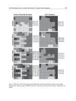
Probe # CF |CF| ∠CF(de g)
1 0.8704+j0.0218 0.8706 1.4347
2 0.9645-j0.0806 0.9678 4.7724
3 0.959-j0.0511 0.9603 -3.050
4 1+j0 1 0
5 1.0007-j0.0091 1.0007 -0.5210
6 1.0252+j0.0258 1.0255 1.4415
7 1.0432+j0.0406 1.0439 2.2287
Table 1. The measurement results of a known field using individual probes (all
measurements have been normalized to the reading of probe #4).
In this experiment, an antenna with a highly concentrated near-field distribution was used as
a DUT. This antenna incorporates a cylindrical waveguide loaded with a dielectric material
having a dielectric constant about 15. This dielectric part concentrates the fields over a small
area where the probe under test is located, while weakly illuminating the other probes (which
are switched OFF). The probes are positioned within the illuminated region near the antenna
and the fields in the E-plane of the illuminating antenna are scanned. Ideally, it is expected that
the probes will measure the same field distribution. However, due to the factors mentioned
earlier they do not. Therefore, as an effective compensation technique, a probe in the array is
used as a reference (e.g., probe#4, central) to which the rest of the probes are weighted by a
complex number (e.g., correction factor). The correction factors can be obtained for several
points and averaged to get a better agreement between the responses of the probes. The
computed correction factors based on the method explained here, are listed in Table 1. The
effect of applying correction factors on the measurement results will be discussed later.
97
Low Scattering Photodiode-Modulated Probe for Microwave Near-Field Imaging
20 Photodioes
12.2 Receiving antenna compensation
In the bistatic test setup, the receiving part of the NF imager incorporates an auxiliary antenna
(AA) to pick up the scattered fields and send them to the coherent detector, as illustrated
in Fig. 20b (see also Fig. 1). During the scan, the AA is moved together with the array
and its phase centre has a minimum distance from the central probe (i.e., probe#4). In this
configuration, the rest of the probes are placed symmetrically on both sides of probe #4. As can
be observed in Fig. 20b, the scattered fields propagate along different paths to reach the AA
(i.e., r
i
; i=1, 7). Each probe is also seen by the AA with a different view. Then, the picked-up
signals will not be identical even if all the probes are exposed to the same fields. So, we
need to compensate the measured data (raw data) for the NF radiation pattern of the AA.
In principle, the simple compensation method described in the previous subsection should
suffice. In practice however it has been observed that the coupling between each probe and the
AA slightly varies when the probes are moved near the AUT, even if the AA is maintained at
a fixed position with respect to the probe array. This variation comes from mutual interaction
of the AA and probe array with the AUT, which is not constant during the scan. A method to
compensate for this effect is introduced in the next paragraph. We first set the AA in Fig. 20b
(a) Magnitude (b) Phase
Fig. 21. The measurement result obtained in the test to compensate for the radiation pattern
of the receiving antenna; (a) magnitude and (b) phase of the normalized measured E field by
the AA in the monostatic setup.
to operate as an illuminator in a monostatic mode (TX/RX device). During this test the AUT
is passive and terminated with a matched load. In this experiment, the probes are addressed
successively and then moved to a new position until the array scans the region of interest
above the AUT. Ideally, a flat response is expected over the region scanned by each probe, but
given the interaction of the array with the surrounding objects, including the passive AUT,
and the interaction between probes, the measured results are not constant, as illustrated in
Fig. 21. In this test the AUT was a horn antenna and the array was scanned at a height of
30 mm (i.e., λ/4) above the aperture. The ideal results, i.e., with no interaction between the
probes with the AUT and the AA are shown by broken line in Fig. 21. The asymmetry of the
curves occurs because of discrepancies in the probes of the array, displacement of probes and
misalignment. Even though each probe is at a fixed distance and angle from the receiving
antenna, significant variation can be observed when a 30 mm interval is scanned. The results
also demonstrate the importance of the compensation before any comparison is made to
validate the imager’s results. After this test, the E-field measurements of the AA at each
98
Photodiodes – Communications, Bio-Sensings, Measurements and High-Energy Physics
Low Scattering Photodiode-Modulated Probe For Microwave Near-Field Imaging 21
position of the array and for each probe (i.e., E
AA
) are used to correct the NF measurements
obtained for the AUT in the bistatic setup, i.e.,:
E
AUT
=
E
AUT ,Bistatic
E
AA
(18)
13. OMS probes array: validation results
The electric field distribution of a planar inverted-F antenna (PIFA, Fig. 22) radiating at 2.45
GHz was measured in bistatic and monostatic modes on a plane located at λ/4 above the
antenna’s ground plane (Fankem & Melde, 2008). Such an antenna is commonly used in
portable devices (e.g., cellphone) and communication systems.
Fig. 23 shows 2D measurement of the AUT E-field distribution after compensation for probes’
differences, receiving antenna radiation pattern and variations of interactions with the AUT.
The magnitude plot shows a dynamic range of
∼25 dB over a scan area of 240 mm by 210
mm. Fig. 24 shows E- and H-planes NF cuts of the PIFA, including the measured magnitude
and phase. For validating the results obtained by the imager, all measurements are compared
with simulations and also to the field distribution obtained by the imager operating in the
monostatic mode. All curves (i.e., magnitude of E-field) are in good agreement with each
other except that of the monostatic measurement, which deviates from the true field starting
from -20 mm toward negative x values.
Fig. 22. Antenna under test (AUT). PIFA antenna operating at 2.45 GHz with measured
return-loss of about 12 dB; the physical dimensions of the PIFA are as follows: L
p
=27 mm,
W
p
=13 mm, H
p
=7 mm, P
exc
=7 mm, W
GND
=70 mm and L
GND
=137 mm.
In all cases the measured phase information in the E-plane of the PIFA are in good agreement
over the whole x interval. In order to quantify the difference between the measurement results
and the simulated distribution of the PIFA, the mean square error of the data was calculated.
The error associated with E-plane and H-plane cuts are 0.12% and 0.06%, respectively, with
respect to simulations. The benefit of probe correction in the bistatic case is clearly visible in
the H-plane results.
99
Low Scattering Photodiode-Modulated Probe for Microwave Near-Field Imaging
22 Photodioes
(a) Magnitude (b) Phase
Fig. 23. 2-D map of electric field distribution measured (compensated results) at a distance of
λ/4 above AUT; (a) magnitude (dB) and (b) phase (deg.).
(a) E-plane (magnitude) (b) E-plane (phase)
(c) H-plane (magnitude) (d) H-plane (phase)
Fig. 24. E- and H-plane cuts of the measured E-field at distance of λ/4 from the PIFA
antenna’s ground plane; (a) and (c) magnitude (dB), and (b) and (d) phase (deg.).
14. Carrier cancellation: NF imager dynamic range and linearity improvement
In an MST-based NF imager the received signals (modulated) consist of a carrier and
sidebands. Although the probe reflects the field at the carrier frequency, this does not affect
100
Photodiodes – Communications, Bio-Sensings, Measurements and High-Energy Physics
Low Scattering Photodiode-Modulated Probe For Microwave Near-Field Imaging 23
the measurements, which are performed at the sideband frequencies. The carrier is generally
stronger (e.g.,
∼ 50dB) than the sidebands in the modulated signal. Nonlinear behaviour
such as saturation and compression in the receiver occurs at higher powers of the carrier,
particularly beyond -3 dBm.
To overcome these problems, the NF imager can be equipped with an automated circuit,
so-called the carrier canceller, in order to eliminate the carrier from the received signals and
leave the sidebands intact. This allows us to amplify the signal applied to AUTs, leading to
a higher sideband level. As a consequence, the signal-to-noise (SNR) ratio of the modulated
signals at the coherent detector’s front-end improves considerably, resulting in larger dynamic
range. The carrier at the receiving port is minimized by combining the received signal with
a 180-degree out-of-phase tone at the carrier frequency whose magnitude and phase are
adjusted adaptively.
14.1 High-dynamic range NF imager: Example of application
In order to demonstrate the high dynamic range of the NF imager when it is equipped with
the carrier cancellation circuit, the E-field distribution above a bandpass filter operating at
2.45 GHz was measured. The measurement was performed 3 mm above the traces at 2.45
GHz. Figure 25a shows photograph of the filter under test. The results shown in Figure 25b-c
include both magnitude and phase of E
x
. It can be seen, that the power propagate through
the filter to reach the matched load. The achieved dynamic range of the near-field map is
approximately 80 dB.
15. Conclusions
This chapter addressed and discussed the design and implementation of a NF imager
based on the modulated scatterer technique (MST) in detail. The imager consists of several
optically modulated scatterer (OMS) probes that are very accurate, highly sensitive and also
frequency selective. Each OMS probe was optimized to operate at 2.45 GHz. This probe,
guarantees almost perturbation-free measurements. It can be implemented with low-cost
commercial off-the-shelf photodiodes. The OMS probes were also studied and verified
for omnidirectionality and cross-polarization rejection performance. The probes showed
an absolute deviation of about
±0.3 dB with respect to an omnidirectional response. The
co-to-cross polarization ratio was measured and found to be better than 60 dB. The frequency
response of the probe was studied theoretically and experimentally in order to qualify the
performance of the matching network and to assess its impact on the frequency response of the
OMS probes. The performance of the probes was validated by measuring the NF distribution
of a 50 Ω microstrip transmission line. The measurements were compared with results of
simulations using HFSS. The results also showed that the sensitivity of the measurement
system can be as low as 0.037 V/m. Error associated with magnitude and phase measurement
of respectively 6.4% and 3.2 degrees were observed. By developing a linear array of OMS
probes, the measurement speed for an E-field measurement was increased more than 14
times compared to that obtained with a commercially available opto-mechanically switched
systems. To improve the accuracy of measurements using the array, the raw measurement
data were corrected using the proposed calibration technique, to compensate for uncertainties
in the probes’ responses. The E-field measurements made with the developed imager were
in good agreement with the simulations and were very rapid. Benefiting from carrier
101
Low Scattering Photodiode-Modulated Probe for Microwave Near-Field Imaging
cancellation, the isolation between the input and output ports of the imager was improved
by about 60 dB. This enabled us to increase the signal fed to the NF imager and reach an
overall dynamic range of 85 dB, i.e., an increase of 18 dB compared to the case when the NF
imager is not equipped with the carrier cancellation circuit.
16. References
Bassen, H. & Smith, G. (1983). Electric field probes–a review, Antennas and Propagation, IEEE
Transactions on 31(5): 710–718.
Baudry, D., Arcambal, C., Louis, A., Mazari, B. & Eudeline, P. (2007). Applications of
the near-field techniques in emc investigations, Electromagnetic Compatibility, IEEE
Transactions on 49(3): 485–493.
Bokhari, S., Zurcher, J F., Mosig, J. & Gardiol, F. (1995). Near fields of microstrip antennas,
Antennas and Propagation, IEEE Transactions on 43(2): 188–197.
Bolomey, J. & Gardiol, F. (2001). Engineering applications of the modulated scatterer technique,
Artech House.
(a)
(b) (c)
Fig. 25. The measurement results of the transverse E-field above a bandpass filter at 2.45
GHz; (a) magnitude and (b) phase.
102
Photodiodes – Communications, Bio-Sensings, Measurements and High-Energy Physics
Low Scattering Photodiode-Modulated Probe For Microwave Near-Field Imaging 25
Budka, T., Waclawik, S. & Rebeiz, G. (1996). A coaxial 0.5-18 ghz near electric
field measurement system for planar microwave circuits using integrated probes,
Microwave Theory and Techniques, IEEE Transactions on 44(12): 2174–2184.
Cown, B. & Ryan, C.E., J. (1989). Near-field scattering measurements for determining complex
target rcs, Antennas and Propagation, IEEE Transactions on 37(5): 576–585.
Dubois, T., Jarrix, S., Penarier, A., Nouvel, P., Gasquet, D., Chusseau, L. & Azais, B.
(2008). Near-field electromagnetic characterization and perturbation of logic circuits,
Instrumentation and Measurement, IEEE Transactions on 57(11): 2398–2404.
Fankem, B. & Melde, K. (2008). Nested pifas for dual mode of operation: Gps and global
communications, Antennas and Wireless Propagation Letters, IEEE 7: 701–705.
Hygate, G. (1990). Measuring microwave fields with a minimum of perturbation, Precision
Electromagnetic Measurements, 1990. CPEM ’90 Digest., Conference on, pp. 198–199.
Hygate, G. & Nye, J. F. (1990). Measuring microwave fields directly with an optically
modulated scatterer, Measurement Science and Technology 1(8): 703–709.
Iigusa, K., Sawaya, T., Taromaru, M., Ohira, T. & Komiyama, B. (2006). Experimental
proof of electrically invisible state of inductively loaded dipole and proposal of
electrically invisible meander-lines, Antennas and Propagation, IEEE Transactions on
54(11): 3374–3382.
Justice, R. & Rumsey, V. (1955). Measurement of electric field distributions, Antennas and
Propagation, IRE Transactions on 3(4): 177–180.
King, R. J. (1978). Microwave Homodyne System, Wiley New York.
Laurin, J J., Zurcher, J F. & Gardiol, F. (2001). Near-field diagnostics of small printed antennas
using the equivalent magnetic current approach, Antennas and Propagation, IEEE
Transactions on 49(5): 814–828.
Liang, W., Hygate, G., Nye, J., Gentle, D. & Cook, R. (1997). A probe for making
near-field measurements with minimal disturbance: the optically modulated
scatterer, Antennas and Propagation, IEEE Transactions on 45(5): 772–780.
Mostafavi, M., Bolomey, J C. & Picard, D. (2005). Experimental study on compensation
of array element pattern of collinear dipole array sensor, EICE Trans Commun, Inst
Electron Inf Commun Eng. E88-B(8): 3314–3316.
Munoz, K., Perrey, A. & Zoughi, R. (2008). Potential application of the modulated
scatterer technique to multilayered material evaluation and health monitoring,
Instrumentation and Measurement Technology Conference Proceedings, 2008. IMTC 2008.
IEEE, pp. 1643–1647.
Nye, J. (2003). A simple method of spherical near-field scanning to measure the far fields
of antennas or passive scatterers, Antennas and Propagation, IEEE Transactions on
51(8): 2091–2098.
Omrane, B., Laurin, J J. & Goussard, Y. (2006). Subwavelength-resolution microwave
tomography using wire grid models and enhanced regularization techniques,
Microwave Theory and Techniques, IEEE Transactions on 54(4): 1438–1450.
Petre, P. & Sarkar, T. (1992). Planar near-field to far-field transformation using an
equivalent magnetic current approach, Antennas and Propagation, IEEE Transactions
on 40(11): 1348 –1356.
Quilez, M., Aragon, M., Atienza, A., Fernandez-Chimeno, M., Riu, P. & Silva, F.
(2008). A near-field probe for in situ emi measurements of industrial installations,
Electromagnetic Compatibility, IEEE Transactions on 50(4): 1007–1010.
103
Low Scattering Photodiode-Modulated Probe for Microwave Near-Field Imaging
26 Photodioes
Richmond, J. (1955). A modulated scattering technique for measurement of field distributions,
Microwave Theory and Techniques, IRE Transactions on 3(4): 13–15.
Rogers, P. (1986). Application of the minimum scattering antenna theory to mismatched
antennas, Antennas and Propagation, IEEE Transactions on 34(10): 1223–1228.
Smith, G. (1984). Limitations on the size of miniature electric-field probes, Microwave Theory
and Techniques, IEEE Transactions on 32(6): 594–600.
Tehran, H., Laurin, J J. & Kashyap, R. (2009). A low-perturbation near-field imager equipped
with optical mst probes, Antennas and Propagation, 2009. EuCAP 2009. 3rd European
Conference on, pp. 3649–3653.
Yan, B., Saoudy, S. & Sinha, B. (1997). A low cost planar near-field/far-field antenna
measurement system, Antennas and Propagation Society International Symposium, 1997.
IEEE., 1997 Digest, Vol. 1, pp. 152–155 vol.1.
104
Photodiodes – Communications, Bio-Sensings, Measurements and High-Energy Physics
0
Single Shot Diagnostics of Quasi-Continuously
Pumped Picosecond Lasers Using Fast
Photodiode and Digital Oscilloscope
Michal Jelínek, Václav Kubeˇcek and Miroslav
ˇ
Cech
Czech Technical University in Prague
Czech Republic
1. Introduction
Ultrashort laser pulses with duration in the range between 10 and 100 ps play important
role in many applications, such as microsurgery, micromachining, laser ranging, nonlinear
optics etc. Methods enabling precise measurement of such pulses duration are therefore
essential. Common silicon photodiodes used in combination with ordinary oscilloscopes
cannot be used for such a precise measurement because of low temporal resolution of the
whole system. Therefore, several sophisticated methods based on optical or electro-optical
effects were developed in the past decades and are still widely used (Diels, 1995; Keller,
2007; Rulliere, 2003). The first method based on nonlinear optical effect is measurement of
second order autocorrelation function of the measured light pulse. This function is always
symmetric and does allow to obtain detailed information on the exact pulse shape and pulse
duration is calculated assuming the certain pulse temporal profile. This method, which can
be used either for single or repetitive pulses, is in principle very precise but has also several
disadvantages. The whole measuring system has to be aligned precisely and the measured
beam has to enter the system in accurately aligned angle. Precision depends also on control
of the delay line used for scanning autocorrelation measurement. Because the resulting pulse
length is in this case calculated from many points, it is clear that it represents average value of
the real pulses lengths and is difficult to evaluate pulse duration stability or study some other
effects, i.e. pulse shortening under specific conditions. The single shot autocorrelators on
the other hand can measure the autocorrelation function from only single laser shot but exact
interpretation is not also unique. The only direct picosecond pulses measurement method
based on electro optical effect uses a streak camera. This method allows to measure single
pulse duration and shape but several consecutive pulses in the pulse train cannot be measured
with sufficient temporal resolution. It is also necessary to carefully align whole measuring
system and perform its rigorous calibration including readout.
Repetitive signals as mode locked pulse trains from continuously pumped lasers can be
measured using sampling oscilloscopes in combination with fast detectors enabling resolution
in units of picoseconds. For signals with repetition rates below several kHz sampling
oscilloscopes cannot be used and only real time oscilloscopes with lower resolution are
available. In the past few years fast real time oscilloscopes with analog bandwidth up to
6
2 Will-be-set-by-IN-TECH
40 GHz primarily designed for digital signal processing became available. In combination
with sufficiently fast photodiode (commercially available with bandwidth up to
∼60 GHz) a
powerful tool for single ultrashort laser pulse characterization appeared. The photodiode
- oscilloscope system for measurement of such laser pulses has several advantages. This
procedure is simple to perform because the laser beam can be easily directed on the
photodiode and very precise alignment of the measuring system is not necessary. The
measurement is also repeatable, quick, and moreover duration of several pulses in the train
can be recorded simultaneously from the single laser shot which enables investigation of
special effects, such as pulse shortening in the laser output pulse train (Kubecek, 2009).
Furthermore, oscilloscopes offer sophisticated functions and e.g. pulse duration statistics from
thousands of pulses can be studied.
The subject of this chapter is theoretical and experimental study of the diagnostics of
picosecond laser single pulses and pulse trains with repetition rates below 100 Hz using
measuring system consisting of a fast real time oscilloscope and InGaAs PIN photodiode.
In the first section physics of detection and general properties of photodiodes are described.
In the second section theoretical analysis of pulse duration measurement method using
oscilloscope - photodiode system is performed. Measuring system impulse response based
on calculation from the corresponding datasheet parameters is discussed and subsequently
resulting value is calculated for the given system. The third section deals with experimental
verification of the described measurement method and calculated impulse response. Three
laboratory laser systems based on neodymium (Nd) doped active materials and operated in
quasi-continuously pumped regime were studied. The lasers were passively mode-locked
by the semiconductor saturable absorbers and generated output trains consisted of 5 to
100 pulses. For some measurements single pulse was extracted. The pulses had duration
in the range between 10 and 200 ps depending on the laser system. The pulse duration
was measured simultaneously by our oscilloscope - photodiode system and at least one of
precise optical measuring system (autocorrelator or streak camera) to investigate how short
pulses can be measured with sufficient accuracy. Subsequently, it was possible to use the
measuring system not only for instantaneous estimation of duration of the pulse shorter than
corresponding impulse response, but moreover to investigate pulse duration stability using
oscilloscope sophisticated statistics functions. In addition, two tested laser systems were
operated under special regime resulting in pulse duration shortening along the output pulse
train, which was possible to study precisely at each individual laser shot.
2. Physics of detection and photodiodes
Photodiodes represent one of fundamental light detection devices and play almost
un-substitutable role in many applications, where the time and amplitude characteristic of
the incoming light pulses has to be investigated or further exploited. Among the main
advantages of photodiodes belong ease of use, fast time response, sensitivity at sufficiently
wide spectral region, reasonably low thermal and electrical noise, and small dimensions
enabling integration in electro-optics devices. Photodiodes are mostly used for detection of
laser light pulses in many applications, such as telecommunications, sensing, security, and
laser systems monitoring.
Light detection by a semiconductor material is based on the well-known phenomena of
photon absorption (Saleh, 2007). If the incident photon energy exceeds the band gap energy
106
Photodiodes – Communications, Bio-Sensings, Measurements and High-Energy Physics
Single Shot Diagnostics of Quasi-Continuously Pumped Picosecond Lasers Using Fast Photodiode and Digital Oscilloscope 3
of the semiconductor, an electron-hole pair is released. These charge carriers move by
diffusion to places with lower concentration and may contribute to electrical current, if the
semiconductor is connected into some electrical circuit. Since the diffusion rate is slow, these
photo-conductors cannot be used as sufficiently fast photodetectors.
The situation changes when a photodiode formed by PN junction is used. Between the P
and N regions, there is a depletion layer consisted of positively and negatively charged fixed
ions. These ions form electrical field in the direction from N to P. If the photon is absorbed
in this depletion layer, the electrons and holes are accelerated by the described electrical field.
In this layer the carriers move by drift process which depends on the electrical field and is
much quicker than diffusion. The depletion layer can be further extended applying reverse
bias voltage on the photodiode which significantly decreases the carrier transit time. Reverse
bias voltage (below the breakdown threshold) increases the noise component formed by dark
current. In relation to the detector speed, capacitance formed by the depletion layer has
to be treated and kept as low as possible, because it significantly contributes to the overall
capacitance of the detector therefore influences its RC constant. Depletion layer capacitance is
proportional to its area and inversely proportional to its thickness. Because the area relates
to the photodiode responsivity, there has to be a trade-off between these values and fast
photodiodes have lower sensitivity.
In order to extend the depletion layer, the intrinsic-doped layer can be inserted between P and
N regions forming PIN diode. This leads to reduction of the necessary reverse bias voltage
to several volts and simultaneously to rise the detector speed because most of photons are
absorbed in this layer and generated carriers drift through this layer accelerated by the bias
voltage. Furthermore, thicker depletion layer decreases the junction capacitance.
In the following section photodiode parameters with emphasis on the spectral region and
response time will be discussed from the point of material and construction parameters.
Requested spectral region ranging approximately from 500 to 1500 nm and covers the most
of wavelengths used in solid state lasers enabling ultrashort pulses generation. Spectral
region of the photodiode is mainly limited by its material parameter - the absorption
layer band gap. As the photon absorption does not occur when the incident photon
energy is less than absorption layer band gap E
g
, the long-wavelength component λ
cutof f
is limited by λ
cutof f
= hc/E
g
⇒λ
cutof f
[μm] = 1.24/E
g
[eV]. Therefore, common silicon (Si)
photodiodes can be used for wavelengths only up to
∼1.1 μm. There is also second
well-known semiconductor-compound material - gallium arsenide (GaAs). In the pure form,
its long-wavelength region is limited to about 850 nm. By adding other component, the
wavelength region can be significantly extended. Usage of many compounds has been
published but in the commercially available photodiodes mainly Indium (In) component is
used in the discussed spectral region. Pure InAs has λ
cutof f
of about 3.4 μm and depending
on its concentration in In
x
Ga
1−x
As compound, the wavelength range can be tuned. Mainly
used compound has x
∼0.5 determining λ
cutof f
of ∼1.7 μm (Bitter, 2000).
Usage of GaAs-based material for the PIN photodiode construction has also other advantage
in the charge carrier mobility. The electron mobility in GaAs is about five times higher
than in Si while the hole mobility is comparable (Gibbons, 1987). As for construction
parameters, it has already been said that in order to obtain fast response time it is necessary
to keep the depletion layer capacitance as low as possible. Because of the mentioned
reasons commercially available photodiodes based on GaAs / InGaAs have higher frequency
107
Single Shot Diagnostics of Quasi-Continuously
Pumped Picosecond Lasers Using Fast Photodiode and Digital Oscilloscope
4 Will-be-set-by-IN-TECH
bandwidth in comparison with the silicon photodiodes. The fastest photodiodes for
telecommunication have to be based on InGaAs because of its desirable spectral response
around 1.5 μm.
Besides these standard-type PIN photodiodes there is an extensive effort on the new
photodiodes concepts development and utilization mainly in the telecomunication technique.
Novel high-speed and high-power photodiodes with bandwith higher than 100 GHz were
demonstrated. These new configurations are aimed to overcome the main disadvantages of
the classical PIN photodiodes.
The bandwidth-efficiency and saturation current of the photodiode can be improved using
the Dual-Depletion Region (DDR) detector (Effenberger, 1996). The depletion region of this
structure consists of a InGaAs absorption layer and a InP drift (buffer) layer. This leads to the
reduction of the junction capacitance due to increased depletion layer thickness. Moreover,
the electrons must travel across both InGaAs and InP layers, whereas much slower holes must
travel only across the InGaAs layer resulting in equalization of the transit times for electrons
and holes.
Improved approach is the Uni-Travelling Carrier (UTC) photodiode (Ishibashi, 2000;
Nagatsuma, 2011). This device utilizes only electrons as the active carriers. The active
region consists of a p-InGaAs absorption layer and a wideband i-type carrier-collection
layer. Photo-generated minority electrons diffuse from the absorption layer to the depleted
collection layer, where they are accelerated and transported to the contact. A diffusion barrier
made in the p-InGaAs layer prevents the electrons from diffusing into the p-contact while
the generated holes can diffuse to the contact material. The photo-response is therefore
determined by the electron diffusion time in the absorption layer which can be very thin
leading to high bandwidth. Furthermore, the output peak current increases linearly with
increasing input energy, and the waveform does not significantly change until it reaches the
saturation point. In comparison with the waveform of the PIN photodiode, which consists
from two current components (initial fast component attributed to electron transport and the
slow tail caused by hole transport).
In order to increase the quantum efficiency of the standard (vertically-illuminated) PIN
photodiode, which depends on the absorption layer thickness, a waveguide detection scheme
was used, where the light absorption is perpendicular to current collection (Malyshev,
2004). Using this scheme it is possible to achieve high absorption efficiency and high speed
simultaneously due to the decoupling of the efficiency from the absorption layer thickness.
Efficient operation of these photodiodes based on the thin film germanium on silicon was
successfully demonstrated (Wang, 2008).
Another approach leading to high-speed photodetectors is based on the metal-semiconductor
Schottky junction, mainly developed in the MSM (Metal-Semiconductor-Metal) photodiode
(Berger, 1996; Kache, 2005). Its structure is comprised of back-to-back Schottky diodes that
use an interdigitated electrode configuration on the top of the active absorbing layer. This
construction leads to low capacitance in comparison with the standard PIN photodiodes and
therefore the MSM photodiode response speed is mostly limited by the transit time of the
photo-generated carriers. Different materials may serve as the active layer and besides IR and
visible spectral range also UV detectors were demonstrated successfully (Liu, 2010).
108
Photodiodes – Communications, Bio-Sensings, Measurements and High-Energy Physics
Single Shot Diagnostics of Quasi-Continuously Pumped Picosecond Lasers Using Fast Photodiode and Digital Oscilloscope 5
3. Picosecond pulse measurement using oscilloscope - photodiode system
3.1 Measuring system response
This chapter is aimed at measurement of ultrashort light pulses with duration between 10 and
200 ps generated by mode-locked lasers. The measurement is performed using oscilloscope
- photodiode system and therefore overall response time of these both components has to
be treated. Response time of each electrical component is limited by its electrical frequency
bandwidth which is usually defined at the frequency where a sinusoidal output signal
amplitude is attenuated to about 70 % of its original value (or in other terms the signal power
is attenuated to 50 %), also known as -3 dB point. Let’s consider the pulse width (duration) as
full width at half maxima (FWHM) of light intensity. For the pulse width measurement the
laser pulse shape can be in good approximation considered as Gaussian and therefore sum of
square calculation of the real pulse duration FWHM
REA L
can be used:
FWHM
REA L
=
FWHM
2
MEAS
− FWHM
2
SY STEM
(1)
where FWHM
MEAS
is measured pulse width and FWHM
SY STEM
is the minimal pulse width
(impulse response or response to a Dirac delta function) of the measuring system. This
instrumental constant can be calculated as
FWHM
SY STEM
=
FWHM
2
OSC
+ FWHM
2
PD
(2)
where FWHM
OSC
is the oscilloscope minimal pulse width (given by the oscilloscope impulse
response) and FWHM
PD
is the photodiode minimal pulse width. Into this calculation also
influence of cables and connectors can be included when their frequency bandwidth cannot
be neglected in comparison with other measuring components bandwidth. Similar theorem
can be used for the calculation of rise time (RT) as the system response on the step input signal
(Johnson, 1993; Keller, 2007).
3.2 Minimal pulse width and rise time of the measuring system components
Minimal pulse width FWHM and rise time RT of the measuring components can be calculated
for the given frequency bandwidth f
3dB
according to the formulas
FWHM
=
K
FWHM
f
3dB
, RT =
K
RT
f
3dB
(3)
Constant K varies in range from 0.3 to 0.5 according to the step or impulse response and also
according to calculation performed for the oscilloscope or photodiode.
3.2.1 Photodiode response
The photodiode rise time can be calculated for the given electrical bandwidth using K
RT
= 0.35.
This value is based on the RC element step response and derived for example in (Johnson,
1993; Keller, 2002). It is also accepted by most of photodiode manufacturers who state rise
time value in datasheets according to this calculation. The photodiode impulse response can
be calculated using K
FWHM
= 0.312 which is also derived in (Keller, 2002) and assumes the
Gaussian response.
109
Single Shot Diagnostics of Quasi-Continuously
Pumped Picosecond Lasers Using Fast Photodiode and Digital Oscilloscope
6 Will-be-set-by-IN-TECH
3.2.2 Oscilloscope response
Calculation of the oscilloscope response is little bit more complicated because the constant
K relates to the oscilloscope type. Generally, two types of oscilloscopes are distinguished
according to their shape of frequency response. Analog oscilloscopes and digital oscilloscopes
with 3 dB bandwidth less than 1 GHz usually have Gaussian frequency response. This type of
frequency response slowly decreases towards -3dB attenuation and further. For this type of
oscilloscopes is possible to use similar constants as for the photodiode. However, fast digital
oscilloscopes with higher bandwidth have maximally flat or so-called brick wall response. In
this type the frequency response is much flatter below defined -3dB frequency but then drops
rapidly. These oscilloscopes have several advantages. Signals with frequencies below f
3dB
can be measured more precisely and higher frequency signals do not produce sampling alias
errors. However, for this type of oscilloscope the assumptions and formulas for the Gaussian
pulse are not valid precisely. Also the K
RT
value is higher and ranging from 0.4 to 0.5 (Agilent,
2011; Tektronix, 2009). The K
FWHM
is not precisely defined and according to uncertainty of
K
RT
its value can be just estimated.
3.2.3 Calculation of the measuring system impulse response
According to the previous analysis, the step and impulse response of the measuring system
used in our experiments can be calculated. The measuring system consisted of the PIN
photodiode EOT ET-3500 (EOT, 2011) connected by high frequency SMA cable to the real
time oscilloscope LeCroy SDA-9000 (LeCroy, 2009)
1
. Datasheet parameters of the photodiode
are as following: cutoff frequency >15 GHz, rise and fall time <25 ps, spectral range 1000 -
1650 nm, responsivity 0.88 A/W @ 1550 nm, active area diameter 32 μm, junction capacitance
0.12 pF. Important datasheet parameters as well as rise time and minimal pulse width
calculation are summarized in Table 1.
Compo- Datasheet values Step response Impulse response
nents & f
3dB
RT RT K
FWHM
FWHM K
FWHM
FWHM
System [GHz] [ps] [ps] [ps] [ps]
LeCroy 9.0 <49 49 0.44 49 0.40 45
EOT 15.0 <25 25 0.31 21 0.31 21
System - - 55 - 53 - 50
Table 1. Datasheet values and calculated system response FWHM
SY STEM
.
The system rise time can be calculated directly from the given datasheet values. The minimal
pulse width is calculated from the given frequency bandwidth. For the oscilloscopes two
values of K
FWHM
are used. The first value of 0.44 is the same as used for the step response
calculation, the second value of 0.4 is the estimation based on fact that the impulse response
for the Gaussian systems is about 0.9 times shorter than step response (Andrews, 1989). It can
be seen that the calculated minimal FWHM given by the impulse response is about 50 ps.
1
Trade names are used to specify the experimental setup only.
110
Photodiodes – Communications, Bio-Sensings, Measurements and High-Energy Physics