Organic Light Emitting Diode Material Process and Devices Part 7 ppt
Bạn đang xem bản rút gọn của tài liệu. Xem và tải ngay bản đầy đủ của tài liệu tại đây (2.67 MB, 25 trang )
High Efficiency Red Phosphorescent Organic Light-Emitting Diodes with Simple Structure
141
Gao, Y., Wang, L., Zhang, D., Duan, L., Dong, G. & Qiu, Y. (2003). Bright single-active layer
small-molecular organic light-emitting diodes with a polytetrafluoroethylene
barrier, Appl. Phys. Lett. 82: 155-157.
Giebeler, C., Antoniadis, H., Bradley, D. D. C. & Shirota, Y. (1998). Space-charge-limited
charge injection from indium tin oxide into a starburst amine and its implications
for organic light-emitting diodes, Appl. Phys. Lett. 72: 2448-2450.
Gong, X., Ostrowski, J.C., Moses, D., Bazan, G.C. & Heeger, A.J. (2002). Red
electrophosphorescence from polymer doped with iridium complex, App. Phys.
Lett. 81: 3711-3713.
Gong, X., Ostrowski, J.C., Moses, D., Bazan, G.C. & Heeger, A.J. (2003).
Electrophosphorescence from a polymer guest-host system with an Iridium
complex as guest: Forster energy transfer and charge trapping, Adv. Funct. Mater.
13: 439-444.
Hamada, Y., Sano, T., Fujita, M., Fujii, T., Nishio, Y. & Shibata, K. (1993). High luminance in
organic electroluminescent devices with bis (10-hydroxybenzo [h]quinolinato)
beryllium as an emitter, Chem. Lett. 22: 905-909.
Helfrich, W. & Schneider, W.G. (1965). Recombination Radiation in Anthracene Crystals,
Phys. Rev. Lett. 14: 229-231.
Ho, C.-L., Wong, W.-Y., Wang, Q., Ma, D., Wang, L. & Lin, Z. (2008a). A Multifunctional
Iridium-Carbazolyl Orange Phosphor for High-Performance Two-Element WOLED
Exploiting Exciton-Managed Fluorescence/Phosphorescence, Adv. Funct. Mater. 18:
928-937.
Ho, C.-L., Lin, M.-F., Wong, W.-Y., Wong, W.K. & Chen, C.H. (2008b). High-efficiency and
color-stable white organic light-emitting devices based on sky blue
electrofluorescence and orange electrophosphorescence, Appl. Phys. Lett. 92: 0833011 – 083301-3.
Holmes, R.J., D’Andrande, B.W., Ren, X., Li, J., Thompson, M.E. & Forrest, S.R. (2003).
Efficient, deep-blue organic electrophosphorescence by guest charge trapping,
Appl. Phys. Lett. 83: 3818-3820.
Hong, I-H., Lee, M.-W., Koo, Y.-M., Jeong, H., Kim, T.-S. & Song, O.-K. (2005). Effective hole
injection of organic light-emitting diodes by introducing buckminsterfullerene on
the indium tin oxide anode, Appl. Phys. Lett. 87: 063502-1 – 063502-3.
Huang, J., Yang, K., Liu, S. & Jiang, H. (2000). High-brightness organic double-quantumwell electroluminescent devices, Appl. Phys. Lett. 77: 1750-1752.
Huang, J., Pfeiffer, M., Werner, A., Blochwitz, J., Leo, K. & Liu, S. (2002). Low-voltage
organic electroluminescent devices using pin structures, Appl. Phys. Lett. 80, 139141.
Huang, Q., Cui, J., Yan, H., Veinot, J. G. C. & Marks, T. J. (2002). Small molecule organic
light-emitting diodes can exhibit high performance without conventional hole
transport layers, Appl. Phys. Lett. 81: 3528-3530.
Huang, J., Watanabe, T., Ueno, K. & Yang, Y. (2007). Highly Efficient Red Emission Polymer
Phosphorescent Lighting Emitting Diodes based on two novel Ir(piq)3 derivatives,
Adv. Mater. 19: 739-743.
Hung, L.S., Tang, C.W. & Mason, M.G. (1997). Enhanced electron injection in organic
electroluminescence devices using an Al/LiF electrode, Appl. Phys. Lett. 70: 151-153.
142
Organic Light Emitting Diode – Material, Process and Devices
Ikai, M., Tokito, S., Sakamoto, Y., Suzuki, T. & Taga, Y. (2001). Highly efficient
phosphorescence from organic light-emitting devices with an exciton-block layer,
Appl. Phys. Lett. 79: 156-158.
Jeon, W. S., Park, T. J., Park, J. J., Kim, S. Y., Jang, J., Kwon, J. H. & Pode, R. (2008a). Highly
efficient bilayer green phosphorescent organic light emitting devices, Appl. Phys.
Lett. 92: 113311-1 113311-3.
Jeon, W. S., Park, T. J., Park, J. J., Kim, S. Y., Pode, R., Jang, J. & Kwon, J. H. (2008b). Low rolloff efficiency green phosphorescent organic light-emitting devices with simple
double emissive layer structure, Appl. Phys. Lett. 93: 063303-1 - 063303-3.
Jeon, W.S., Park, T. J., Kim, S. Y., Pode, R., Jang, J. & Kwon, J.-H. (2009). Ideal host and guest
system in phosphorescent OLEDs Org. Electron. 10: 240-246.
Kawamura, Y., Goushi, K., Brooks, J., Brown, J., Sasabe, H. & Adachi, C. (2005). 100%
phosphorescence quantum efficiency of Ir(III) complexes in organic semiconductor
films, Appl. Phys. Lett. 86: 071104-1 – 071104-3.
Kawamura, Y., Brooks, J., Brown, J., Sasabe, H. & Adachi, C., (2006). Intermolecular
Interaction and a Concentration-Quenching Mechanism of Phosphorescent Ir(III)
Complexes in a Solid Film, Phy. Rev. Lett. 96: 017404-1 – 017404-4.
Kido, J. & Lizumi, Y. (1998). Fabrication of highly efficient organic electroluminescent
devices, Appl. Phys. Lett. 73: 2721-2723.
Kim, H.-K., Byun, Y.-H., Das, R. R., Choi, B.-K. & Ahn, P.-S. (2007). Small molecule based
and solution processed highly efficient red electrophosphorescent organic light
emitting devices, Appl. Phys. Lett. 91: 093512-1 – 093512-3.
Kim, J. H., Liu, M. S., Jen, A. K. Y., Carlson, B., Dalton, L. R., Shu, C. F. & Dodda, R. (2003).
Bright red-emitting electrophosphorescent device using osmium complex as a
triplet emitter, Appl. Phys. Lett. 83: 776-778.
Kim, K.-K., Lee, J.-Y., Park, T.-J., Jeon, W.-S., Kennedy, G.P. & Kwon, J.-H. (2010). Small
molecule host system for solution-processed red phosphorescent OLEDs, Synthetic
Met. 160: 631-635.
Kim, S. H., Jang, J. S., Hong, J. M. & Lee, J. Y. (2007). High efficiency phosphorescent organic
light emitting diodes using triplet quantum well structure, Appl. Phys. Lett. 90:
173501-1 – 173501-3.
Kim, S. Y., Jeon, W. S., Park, T. J., Pode, R., Jang, J. & Kwon, J. H. (2009). Low voltage
efficient simple p-i-n type electrophosphorescent green organic light-emitting
devices, Appl. Phys. Lett. 94: 133303-1 – 133303-3.
Kim, T.-H., Lee, H. K., Park, O. O., Chin, B. D., Lee, S.-H. & Kim, J. K. (2006). White-LightEmitting Diodes Based on Iridium Complexes via Efficient Energy Transfer from a
Conjugated Polymer, Adv. Fun. Mater. 16: 611-617.
Koo, Y.-M., Choi, S.-J., Chu, T.-Y., Song, O.-K., Shin, W.-J., Lee, J.-Y., Kim, J. C. & Yoon, T.-H.
(2008). Ohmic contact probed by dark injection space-charge-limited current
measurements, J. Appl. Phys. 104: 123707-1 – 123797-4.
Kwong, R.C., Nugent, M.R., Michalski, L., Ngo, T., Rajan, K., Tung, Y.-J., Weaver, M.S.,
Zhou, T.X., Hack, M., Thompson, M.E., Forrest, S.R. & Brown, J.J. (2002). High
operational stability of electrophosphorescent devices, Appl. Phys. Lett. 81: 162-164.
High Efficiency Red Phosphorescent Organic Light-Emitting Diodes with Simple Structure
143
Lamansky, S., Djurovich, P., Murphy, D., Abdel-Razzaq, F., Lee, H.-E., Adachi, C. Burrows,
P.E., Mui, B., Forrest, S.R. & Thompson, M.E. (2001). Highly Phosphorescent BisCyclometalated Iridium Complexes: Synthesis, Photophysical Characterization,
and Use in Organic Light Emitting Diodes, J. Am. Chem. Soc. 40: 4304-4312.
Lee, T.-C., Chang, C.-F., Chiu, Y.-C., Chi, Y., Chan, T.-Y., Cheng, Y.-M., Lai, C.-H., Chou, P.T., Lee, G.-H., Chien, C.-H., Shu, C.-F. & Leonhardt, J. (2009). Syntheses,
photophysics, and application of iridium(III) phosphorescent emitters for highly
efficient, long-life organic light-emitting diodes, Chemistry – An Asian Journal 4: 742753.
Lee, J.-H., Lin, T.-C., Liao, C.-C. & Yang, F. H. (2005). Study on organic light-emitting device
with more balanced charge transport, Proc. of SPIE 5632: 220-225.
Li, F., Cheng, G., Zhao, Y., Feng, F. & Liu, S.Y. (2003). White-electrophosphorescence devices
based on rhenium complexes, Appl. Phys. Lett. 83: 4716-4719.
Liu, J., Zhou, Q., Cheng, Y., Geng, Y., Wang, L., Ma, D., Jing, X. & Wang, F. (2006). White
electrolumineseence from a single-polymer system with simultaneous two-color
emission, Polyfluorene as the blue host and a 2,1,3-benzothiadiazole derivative as
the orange dopant on the main chain, Adv. Funct.Mater. 16: 957-965.
Liu, S. W., Huang, C. A., Lee, J. H., Yang, K. H., Chen, C. C. & Chang, Y. (2004). Blue mixed
host organic light emitting devices, Thin Solid Films 453-454: 312-315.
Liu, Y., Guo, J., Feng, J., Zhang, H., Li, Y. & Wang, Y. (2001). High-performance blue
electroluminescent devices based on hydroxyphenyl-pyridine beryllium complex,
Appl. Phys. Lett. 78: 2300-2302.
Liu, Z. W., Helander, M. G., Wang, Z. B. & Lu, Z. H. (2009). Efficient bilayer phosphorescent
organic light-emitting diodes: Direct hole injection into triplet dopants, Appl. Phys.
Lett. 94, 113305-1 – 113305-3.
Liu, Z., Helander, M. G., Wang, Z. & Lu, Z. (2009). Efficient single layer RGB
phosphorescent organic light-emitting diodes, Organic Electron.10: 1146-1151.
Liu, S. W., Lee, J. H., Lee, C. C., Chen, C. T. & Wang, J. K. (2007). Charge carrier mobility of
mixed-layer organic light-emitting diodes, Appl. Phys. Lett. 91: 142106-1 – 142106-3.
Meyer, J., Hamwi, S., Bülow, T., Johannes, H.-H., Riedl, T. & Kowalsky, W. (2007). Highly
efficient simplified organic light emitting diodes, Appl. Phys. Lett. 91: 113506-1 –
113506-3.
Mi, B. X., Wang, P. F., Gao, Z. Q., Lee, C. S., Lee, S. T., Hong, H. L., Chen, X. M., Wong, M. S.,
Xia, P. F., Cheah, K. W., Chen, C. H. & Huang, W. (2009). Strong Luminescent
Iridium Complexes with C^N=N Structure in Ligands and Their Potential in
Efficient and Thermal-stable Phosphorescent OLEDs, Adv. Mater. 21: 339-343.
Ohmori, Y., Kajii, H. & Hino, Y. (2007). Organic Light-Emitting Diodes Fabricated by a
Solution Process and Their Stress Tolerance, J. of Display Technology 3: 238-244.
Park, T.-J., Jeon, W.-S., Park, J.-J., Kim, S.-Y., Lee, Y.-K., Jang, J., Kwon, J.-H. & Pode, R.
(2008). Efficient simple structure red phosphorescent organic light emitting devices
with narrow band-gap fluorescent host, Appl. Phys. Lett. 92: 113308-1 – 113308-3.
Pfeiffer, M., Forrest, S.R., Leo, K. & Thompson, M.E. (2002). Electrophosphorescent p-i-n
organic light-emitting devices for very-high- efficiency flat-panel displays, Adv.
Mater. 14: 1633-1636.
144
Organic Light Emitting Diode – Material, Process and Devices
Pode, R., Kim, K.-H., Kwon, J.-H., Lee, S.-J., Shin, I.-A. & Jin, S.-H. (2010). Solution processed
efficient orange phosphorescent organic light-emitting device with small molecule
host, J Phys. D: Appl. Phys. 43: 025101-1 – 025101-5.
Pode, R., Ahn, J.-S., Jeon, W. S., Park, T. J. & Kwon, J.-H. (2009). Efficient red light
phosphorescence emission in simple bi-layered structure organic devices with
fluorescent host-phosphorescent guest system, Current Applied Physics 9, 1151-1154.
Pope, M., Kallmann, H.P. & Magnante, P. (1963). Electroluminescence in Organic Crystals,
The Journal of Chemical Physics 38: 2042- 2043.
Qiu, Y., Gao, Y., Wei, P. & Wang, L. (2002a). Organic light-emitting diodes with improved
hole-electron balance by using copper phthalocyanine/aromatic diamine multiple
quantum wells, Appl. Phys. Lett. 80: 2628-2630.
Qiu, Y., Gao, Y., Wang, L., Wei, P., Duan, L., Zhang, D. & Dong, G. (2002b). High-efficiency
organic light-emitting diodes with tunable light emission by using aromatic
diamine/5,6,11,12-tetraphenylnaphthacene multiple quantum wells, Appl. Phys.
Lett. 81: 3540-3542.
Ramos-Ortiz, G., Oki, Y., Domercq, B. & Kippelen, B. (2002). Förster energy transfer from a
fluorescent dye to a phosphorescent dopant: a concentration and intensity study,
Physical Chemistry Chemical Physics (RSC Publishing) 4: 4109-4114.
Sheats, J. R., Antoniadis, H., Hueschen, M., Leonard, W., Miller, J., Moon, R., Roitman, D. &
Stocking, A. (1996). Organic Electroluminescent Devices, Science 273: 884-888.
Shirota, Y., Kuwabara, Y., Inada, H., Wakimoto, T. , Nakada, H., Yonemoto, Y., Kawami, S.
& Imai, K. (1994). Multilayered organic electroluminescent device using a novel
starburst molecule, 4,4′,4″-tris(3-methylphenylphenylamino)triphenylamine, as a
hole transport material, Appl. Phys. Lett. 65: 807-809.
Seo, J.H., Park, J.H., Kim, Y.K., Kim, J.H., Hyung, G.W., Lee, K.H. & Yoon, S.S. (2007).
Highly efficient white organic light-emitting diodes using two emitting materials
for three primary colors (red, green, and blue), Appl. Phys. Lett. 90: 203507-1 –
203507-3.
Shen, Z., Burrows, P. E., Bulovic, V., Forrest, S. R. & Thompson, M. E. (1997). Three-Color,
Tunable, Organic Light-Emitting Devices, Science 276: 2009-2011.
Shoustikov, A., You, Y., Burrows, P.E., Thompson, M.E. & Forrest, S.R. (1997). Orange and
red organic light-emitting devices using aluminum tris(5-hydroxyquinoxaline),
Synth. Met. 91, 217-221.
Tanaka, D., Sasabe, H., Li, Y.J., Su, S.-J., Takeda, T. & Kido, J. (2007). Ultra High Efficiency
Green Organic Light-Emitting Devices, Jpn. J. Appl. Phys. 2 Lett. (Japan) 46: L10L12.
Tanaka, I. & Tokito, S. (2008). Energy-transfer processes between phosphorescent guest and
fluorescent host molecules in phosphorescent OLEDs, Edited by H. Yersin, Highly
efficient OLEDs with Phosphorescent materials, Wiley –VCH verlag GmbH & Co.
KGaA, Weinheim.
Tanaka, I., Tabata, Y. & Tokito, S. (2004). Energy-transfer and light-emission mechanism of
blue phosphorescent molecules in guest-host systems, Chem. Phys. Lett. 400: 86-89.
Tang, C.W., Chen, C. H. & Goswami, R. (1988). Electroluminescent device with modified
thin film luminescent zone, US Patent No. 4 769 292.
High Efficiency Red Phosphorescent Organic Light-Emitting Diodes with Simple Structure
145
Tse, S. C., Tsung, K. K. & So, S. K. (2007). Single-layer organic light-emitting diodes using
naphthyl diamine, Appl. Phys. Lett. 90: 213502-1 – 213502-3.
Tse, S. C., Tsang, S. W. & So, S. K. (2006). Polymeric conducting anode for small organic
transporting molecules in dark injection experiments, J. Appl. Phys. 100: 063708-1 –
063708-5.
Tsuboi, T., Jeon, W. S. & Kwon, J. H. (2009). Observation of phosphorescence from
fluorescent organic material Bebq2 using phosphorescent sensitizer, Opt. Mater. 31:
1755-1758.
Tsuboyama, A., Iwawaki, H., Furugori, M., Mukaide, T., Kamatani, J., Igawa, S., Moriyama,
T., Miura, S., Takiguchi, T., Okada, S., Hoshino, M. & Ueno, K. (2003). Homoleptic
Cyclometalated Iridium Complexes with Highly Efficient Red Phosphorescence
and Application to Organic Light-Emitting Diode, J. Am. Chem. Soc. 125: 1297112979.
Tsujimoto, H., Yagi, S., Asuka, H., Inui, Y., Ikawa, S., Maeda, T., Nakazumi, H. & Sakurai, Y.
(2010). Pure red electrophosphorescence from polymer light-emitting diodes doped
with highly emissive bis-cyclometalated iridium(III) complexes, J. of Organometallic
Chemistry 695: 1972-1978.
Tsuzuki, T. & Tokito, S. (2008). Highly Efficient Phosphorescent Organic Light-Emitting
Diodes Using Alkyl-Substituted Iridium Complexes as a Solution-Processible Host
Material, Appl. Phys. Express 1: 02185-1 – 02185-3.
Tsuzuki, T. & Tokito, S. (2007). Highly Efficient, Low-Voltage Phosphorescent Organic
Light-Emitting Diodes Using an Iridium Complex as the Host Material, Adv. Mater.
19: 276-280.
Tsuzuki, T., Shirasawa, N., Suzuki, T. & Tokito, S. (2003). Color tunable organic lightemitting diodes using pentafluorophenyl-substituted iridium complexes, Adv.
Mater. 15: 1455-1458.
Turro, N. J. (1991a). Modern Molecular Photochemistry, University Science Books, USA, pp
305.
Turro, N.J. (1991b). Modern Molecular Photochemistry, University Science Books, USA, pp
186.
VanSlyke, S. A. & Tang, C.W. (1985). Organic electroluminescent devices having improved
power conversion efficiencies, US Patent 4539507.
VanSlyke, S. A., Chen, C.H. & Tang, C.W. (1996). Organic electroluminescent devices with
improved stability, Appl. Phys. Lett. 69: 2160-2162.
Vanslyke, S. A., Tang, C. W., O’brien, M. E. & Chen, C. H. (1991). Electroluminescent device
with organic electroluminescent medium, US Patent 5061569.
Wakimoto, T., Fukuda, Y., Nagayama, K., Yokoi, A., Nakada, H. & Tsuchida, M. (1997).
Organic EL Cells Using Alkaline Metal Compounds as Electron Injection Materials,
IEEE Trans. Electron Devices 44: 1245-1248.
Wang, H. F., Wang, L. D., Wu, Z. X., Zhang, D. Q., Qiao, J., Qui, Y. & Wang, X. G. (2006).
Efficient single-active-layer organic light-emitting diodes with fluoropolymer
buffer layers, Appl. Phys. Lett. 88: 131113-1 – 131113-3.
Williams, E. L. , Haavisto, K., Li, J. & Jabbour, G. E. (2007). Excimer-Based White
Phosphorescent Organic Light-Emitting Diodes with Nearly 100% Internal
Quantum Efficiency, Adv. Mater. 19: 197-202.
146
Organic Light Emitting Diode – Material, Process and Devices
Zhou, X., Nimoth, J. B., Pfeiffer, M., Maennig, B., Drechsel, J., Werner, A. & Leo, K. (2003).
Inverted transparent multi-layered vacuum deposited organic light-emitting diodes
with electrically doped carrier transport layers and coumarin doped emissive layer,
Synth. Met. 138: 193-196.
5
Organic Field-Effect Transistors Using
Hetero-Layered Structure with OLED Materials
Ken-ichi Nakayama, Yong-Jin Pu, Junji Kido and Masaaki Yokoyama
Yamagata University, Osaka University
Japan
1. Introduction
In recent years, organic transistors have attracted much attention due to their advantages in
developing low-cost, flexible, and large-area production. So far, many kinds of organic
materials have been reported to achieve high-performance organic field-effect transistors
(OFETs). There are two types of organic semiconductors, p-type and n-type, whose majority
carriers are holes and electrons, respectively. For logic gates application, both types and
similar performance OFETs are required for CMOS application. Pentacene is the most
popular material in p-type OFET, and many kinds of polymer materials are also reported
(McCulloch et al., 2006). On the other hand, the performance of n-type OFETs is generally
inferior to that of p-type (Dimitrakopoulos and Malenfant, 2002). In particular, stability in
air is the most serious problem in n-type OFET. Fullerene is the most standard n-type
material showing the highest mobility (Singh et al., 2007); however, the device cannot
operate in air.
There are two guidelines to achieve high mobility and high stability in n-type OFET. One is
to develop a new material having deeper LUMO level. Oxygen and water deteriorate OFET
performance by accepting electrons from the semiconductor molecule. Therefore, enough
deep LUMO level is an efficient way to avoid effect of oxygen or water. In fact, there have
been many materials having deep LUMO levels, for example, perylene bisimide compound,
fullerene derivatives, fluorinated compounds, and so on.
The other important point is surface treatment of the insulator. The field-effect mobility of
the organic semiconductor is strongly affected by the device fabrication process. Various
methods on surface treatments have been reported to improve the carrier mobility. The
HMDS treatment is a standard and efficient way to make the surface hydrophobic (Lin et al.,
1997; Lim et al., 2005). Organic semiconductor can aggregate with high crystallinity on the
hydrophobic surface without influence of the substrate surface. These methods were
developed in p-type OFETs; however, they are also efficient to improve the mobility and
stability of n-type OFETs. Recently, it has been pointed out that low mobility and instability
in air of n-type organic semiconductor is attributed to the surface electron traps of the gate
insulator, and if electron traps can be perfectly eliminated, almost organic semiconductors
can be operate in n-type mode (Chua et al., 2005). Therefore, it has been believed that the
gate insulator surface should be as possible as inert to achieve high mobility and stability in
n-type OFETs.
148
Organic Light Emitting Diode – Material, Process and Devices
In this chapter, we introduce a new concept of a hetero-layered OFET to improve the
performance of OFETs instead of conventional surface treatment methods. The heterolayered OFET includes an interfacial layer of electronic active organic semiconductor having
opposite transport polarity between the insulator and channel layer. For the interfacial layer
of n-type OFET, we employed various types of hole transporting material, which are
generally used for organic light-emitting diodes (OLEDs). For p-type OFET, electron
transporting material was employed.
Such a hetero-layered OFETs composed of p-type and n-type organic semiconductors have
been studied for ambipolar organic transistors, which aimed at the simple inverter circuit or
organic light-emitting transistors (Rost, 2004; Rost et al., 2004). On the other hand, our
proposed hetero-layered OFET employs charge transport material of OLEDs. They generally
form amorphous films resulting in no FET operation by themselves.
The proposed hetero-layered OFET showed improvement of the mobility compared to the
conventional surface treatment. In addition, we found that the stability in air was drastically
improved in n-type OFET by using a hole transporting material having higher HOMO level.
We discuss the relationship between the OFET performance and the electronic property of
the interfacial layer.
2. Perylene bisimide and hole transporting materials
In this section, we will introduce the results of perylene bisimide (PTCDI-C8H) for the
channel layer and the hole transporting material of NPD, TAPC and m-MTDATA for the
interfacial layer. Perylene bisimide compounds are promising n-type organic semiconductor
having deep LUMO levels and high crystallinity. In particular, PTCDI with long alkyl
chains bring about a highly ordered film structure, and very high electron mobility has been
reported (Tatemichi et al., 2006). On the other hand, NPD and TAPC having triphenyl amine
structure are very standard hole transporting material for OLED devices. They show
comparably high hole mobility and good film formation.
Figure 1 shows the hetero-layered structure OFET with top contact and the molecular
structures of m-MTDATA and NPD. Organic transistors were fabricated on a heavily doped
Si substrate with SiO2 layer (300 nm) that works as a common gate electrode. The interfacial
semiconductor layer of m-MTDATA and NPD (20 nm ~ 30 nm) were deposited by
thermal evaporation. For the comparison, the substrates with well-known surface
treatment by octadecyltrichlorosilane (OTS) and hexamethyldisilazane (HMDS) were also
prepared. Au source and drain electrodes were deposited through a shadow mask.
Channel length and width were defined to be 50 μm and 5.5 mm, respectively. The
current modulation of OFETs were measured by a semiconductor parameter analyzer in
the glove box, where the concentration of oxygen and water were less than 1 ppm. The
field-effect mobility, threshold voltage and on/off ratio were estimated from the equation
of saturation regime, ID=[(WCμ)/2L](VG − VT)2, where C is the capacitance per unit area
of the gate dielectrics, W is the channel width, L is the channel length, μ is the carrier
mobility, and VT is the threshold voltage.
Figure 2 shows the transfer characteristics of OFETs with an interfacial layer of NPD, those
subjected to HMDS surface treatment, and those without any interfacial layer and not
subjected to surface treatment (None). In all the devices, the source-drain current (ID)
increased with the positive gate voltage (VG), which indicates that these OFETs operate only
in the n-type mode, and the hole-transporting layer does not acts as a p-type channel layer.
149
Organic Field-Effect Transistors Using Hetero-Layered Structure with OLED Materials
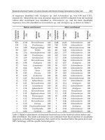
The performances of OFETs with different interfacial layers are summarized in Table 1. The
optimum thickness of the interfacial layer is also indicated. The mobility was improved with
increasing thickness of the hole transporting layer and showed a maximum around 20 nm.
The mobility for heterolayered device was estimated assuming the gate capacitance of only
SiO2 because it is difficult to determine the channel interface. The conventional HMDS
treatment resulted in an improvement in the mobility from 2.5 × 10⁻² cm2/Vs (None) to 6.9 ×
10–2 cm2/Vs. Interfacial layers composed of NPD and m-MTDATA increased the mobility
up to 0.11 and 0.13 cm2/Vs, respectively.
O
C
Drain
O
C
N C 8 H17
C
O
C8 H17 N
Source
C
O
N
N
N
PTCDI-C8H (50nm)
NPD
N
Gate insulator (SiO2)
N
Hole transport layer
Gate (Si)
N
N
N
m-MTDATA
TAPC
Fig. 1. Device structure of hetero-layered OFET using PTCDI-C8H and hole transporting
materials.
0.009
-4
1/2
-5
10
with NPD
with HMDS
none
Drain current (A )
Drain current (A)
10
-6
10
-7
10
-8
10
-9
10
-20
-10
0
10
20
30
Gate voltage / V
40
50
with NPD
with HMDS
none
0.008
0.007
0.006
0.005
0.004
0.003
0.002
0.001
0.000
0
10
20
30
40
50
Gate voltage / V
Fig. 2. Transfer characteristics of the n-type OFET with hetero-layered structure and
conventional surface treatment.
These results indicate that an electronically active material can be used to fabricate an
interfacial layer, and high performance can be achieved without a surface treatment of selfassembly monolayer. We also investigated some other organic materials, n-hexatriacontane
that is perfectly inert material, and Alq3 that is a well-known emissive and electron
transporting material. In these cases, the mobility was rather reduced to be 10–3 cm2/Vs.
These results enable us to conclude that hole transporting materials are responsible for
enhancing mobility.
Mobility can also be improved by modifying the structure of the semiconductor film. X-ray
diffraction patterns of PTCDI-C8H films with and without the NPD (10 nm) interfacial layer
150
Organic Light Emitting Diode – Material, Process and Devices
were measured under the same condition (Fig. 3). Patterns of both the films showed a very
strong peak at 4.3° corresponding to d = 2.05 nm. This peak is assigned to the long axis of the
molecules, which are aligned vertically on the surface. However, in the case of the PTCDI-C8H
films with the NPD interfacial layer, the diffraction peaks are rather weak, which is also
supported by the fact that the high order peaks become unclear, as shown in the magnified
inset of Fig. 3. This result indicates that the improvement in mobility caused by the holetransporting interfacial layer is not attributed to the increase in crystallinity of the PTCDI-C8H
film. This interpretation is also supported by contact angle measurements. The contact angle of
the interfacial layer was 85.8° for m-MTDATA and 92.5° for NPD. These values are
comparable to that of HMDS-treated SiO2 surface. This fact also indicates that the mobility
improvement can be attributed to the electronic effect of hole transporting layer.
Mobility
(cm V s )
Threshold
(V)
On/off
ratio
Bare
0.0351
20.4
5.18 × 10
HMDS
0.0690
21.5
1.32 × 10
n-hexatriacontane (15 nm)
0.0407
11.8
3.00 × 10
TAPC (20 nm)
0.0713
15.5
1.28 × 10
NPD (10 nm)
0.110
16.7
1.17 × 10
m-MTDATA (20 nm)
0.127
25.3
1.33 × 10
Alq3 (15 nm)
0.00686
12.4
-
Surface
2
-1 -1
3
4
3
4
4
4
Table 1. Performances of PTCDI-C8H OFETs with different interfacial layers between the
gate insulator and the channel layer.
(a) NPD / PTCDI-C8H
(b) PTCDI-C8H
100000
12000
10000
200
8000
100
6000
0
Intensity (cps)
Intensity (cps)
14000
4000
10
20
30
2000
0
5
10
15
20
2 (deg)
25
30
80000
200
60000
100
40000
0
10
20
30
20000
0
5
10
15
20
25
30
2 (deg)
Fig. 3. X-ray diffraction patterns of (a) NPD (10 nm)/PTCDI-C8H (50 nm) film and (b)
PTCDI-C8H (50 nm) film deposited on the Si/SiO2 substrate.
Energy levels (highest occupied molecular orbital (HOMO) and LUMO levels) of the organic
semiconductors used in this study are shown in Fig. 4. The n-type organic semiconductor,
Organic Field-Effect Transistors Using Hetero-Layered Structure with OLED Materials
151
PTCDI-C8H, has a deep LUMO level of 4.6 eV. On the other hand, hole transport material of
NPD and TAPC has higher HOMO level and wide energy gap exceeding 3 eV. Therefore,
LUMO level of the interfacial layer is much higher than that of the channel layer.
Electron energy (eV)
1.9
2.5
2.0
3.2
4.6
5.1
m-MTDATA
5.5
NPD
5.6
TAPC
5.9
Alq3
6.6
PTCDI-C8H
Fig. 4. Energy level diagrams of organic semiconductors used in this study. Upper and
lower values indicate the LUMO and HOMO.
These results can be interpreted as following model. Figure 5 shows the schematic energy
diagram of the heterolayered OFET. Since the LUMO level of the interfacial layer was
considerably higher than that of the n-type semiconductor layer, electrons would not enter the
interfacial layer. In addition, the hole-transporting layer did not show p-type FET operation.
Therefore, it was concluded that an n-type channel was formed at the interface between the
hole-transporting layer and the n-type semiconductor film. The role of the interfacial layer can
be basically attributed to the separation of the channel carriers from the surface electron traps,
similar to the conventional hydrophobic surface treatment. However, it was noted that the
mobility or threshold voltage had a correlation with the HOMO level of the inserted layer.
Mobility increased in the order of m-MTDATA > NPD > TAPC, which corresponded to the
order of the HOMO levels, i.e., the interfacial layer with a higher HOMO level exhibited better
performance. This result suggests that the nature of semiconductor of the interfacial layer
affected the electron transportation process at the interfacial channel.
source
gate
n-type
semiconductor
interfacial layer
insulator
Surface traps
of the insulator
N-type channel
Electron traps
in the n-type channel
Fig. 5. Schematic relationship of energy levels in the hetero-layered OFET composed of hole
transporting layer and n-type organic semiconductors.
This additional effect should be discussed from the viewpoint of electronic interaction
between the hole transporting layer and the n-type channel layer. In the single layer device
152
Organic Light Emitting Diode – Material, Process and Devices
of PTCDI-C8H, the surface electron traps of SiO2 can be passivated by inert surface
treatment like HMDS. However, there would be many electron traps in the PTCDI-C8H film
itself. They cannot be eliminated by surface treatment of the substrates. On the other hand,
the hole transporting materials generally have higher HOMO levels, in other words,
electron donating character. Therefore, the interfacial layer tends to give electrons toward
PTCDI-C8H film at the interface. It may not eliminate the shallow electron traps because the
HOMO level of NPD is far from the LUMO level of PTCDI-C8H, but the deep electron traps
are expected to be filled in advance by thermally activated charge transfer. As a result, the
injected electrons can move smoothly at the interface, resulting in the observed high electron
mobility. We conclude that this trap-filling effect is essential of the hetero-layered OFET.
Thus, we proposed the concept of hetero-layered OFETs and ascertained its validity. The
performance was improved by insertion of the electronic active material rather than an inert
surface treatment. Because the film structure of the deposited PTCDI-C8H was not changed
by the surface treatment or interfacial layer, we concluded that this improvement is
attributed to electron donating character of the hole transporting layer.
3. C60 and hole transporting materials
In this section, the concept of hetero-layered OFET is applied to the combination of C60
channel layer and hole transporting material (Fig. 6). C60 is the most standard material of ntype organic semiconductors and the highest performance in n-type OFET has been
reported. The device structure is the same structure with the previous section. For the
interfacial layer, typical hole transporting material of NPD and m-MTDATA were used.
Source
Drain
N
C60 (100 nm)
N
N
SiO2
Si substrate (gate)
N
Hole transport layer
NPD
N
N
m-MTDATA
Fig. 6. Device structure of hetero-layered OFET composed of C60 and hole transporting
materials.
Figure 7 shows the drain current–gate voltage (ID-VG) characteristics of the hetero-layered
OFETs with m-MTDATA and NPD interfacial layer, and the single layer C60 OFETs on OTStreated, HMDS-treated, and non-treated substrates. Also in this case, the ID – VG curves for
the hetero-layered devices increased only for positively biased gate voltage with almost no
hysteresis for forward and backward sweeps. This means that they did not operate as an
ambipolar transistor, and the interfacial layer of the hetero-layered device did not work as a
p-type channel layer.
The performance of each device were summarized in Table 2. The conventional surface
treatment by OTS and HMDS brought about high electron mobility of 0.50 and 0.80 cm2/Vs,
respectively, whereas the normal device on the non-treated substrate showed low mobility
of 7.5 × 10⁻³ cm2/Vs. However, it should be noted that the hetero-layered device with m-
153
Organic Field-Effect Transistors Using Hetero-Layered Structure with OLED Materials
MTDATA and NPD achieved very high electron mobility of 1.1 and 1.8 cm2/Vs,
respectively. These values are the highest value for C60 FETs without any surface treatment
or substrate heating. Thus, it was revealed that the hetero-layered OFET is generally
efficient to improve the performance even in high performance OFETs using C60.
-2
10
-3
10
3.0x10
-2
-4
10
-5
2.5x10
-2
10
-6
2.0x10
-2
10
-7
10
-8
1.5x10
-2
10
-9
10
VD=100V
-10
10
1.0x10
-11
-40
-20
0
20
40
60
80
-2
5.0x10
-3
-1
10
(b)
-2
-2
4.5x10
-3
4.0x10
-4
3.5x10
-5
3.0x10
-6
2.5x10
-7
2.0x10
-8
1.5x10
-9
1.0x10
10
Drain current (A)
3.5x10
-2
-2
10
-2
10
-2
10
-2
10
-2
10
-2
10
10
VD=100V
-10
10
0.0
100 120
-2
10
-11
-40
-20
-4
10
-5
10
-6
10
-7
10
-8
10
Drain current (A)
10
-9
-40
-20
0
20
40
60
-3
0.0
100 120
(d)
-2
-1
-2
10
-3
10
-4
10
-5
10
-6
10
-7
10
-8
10
-9
10
-40
-20
0
20
40
60
6.0x10
-2
5.5x10
-2
5.0x10
-2
4.5x10
-2
4.0x10
-2
3.5x10
-2
3.0x10
-2
2.5x10
-2
2.0x10
-2
1.5x10
-2
1.0x10
VD=100V 5.0x10⁻³
0.0
80 100 120
1/2
-3
80
Drain current (A )
-2
10
60
10
1/2
10
0
-1
40
10
-2
5.5x10
-2
5.0x10
-2
4.5x10
-2
4.0x10
-2
3.5x10
-2
3.0x10
-2
2.5x10
-2
2.0x10
-2
1.5x10
-2
1.0x10
VD=100V 5.0x10⁻³
0.0
80 100 120
Drain current (A )
10
(c)
Drain current (A)
0
20
Gate voltage (V)
Gate voltage (V)
10
0
5.0x10
1/2
4.0x10
1/2
Drain current (A)
10
(a)
-2
Drain current (A )
-1
Drain current (A )
10
Gate voltage (V)
Gate voltage (V)
Fig. 7. Transfer characteristics of OFETs devices of C60 film on the various kinds of surface,
(a) OTS, (b) HMDS, (c) m-MTDATA (20 nm) films, and (d) NPD (30 nm).
Mobility
(cm V s )
Threshold
(V)
On/off
ratio
SiO2
0.0075
66
6.6 × 10
OTS
0.50
23
5.8 × 10
HMDS
0.80
30
1.0 × 10
m-MTDATA
1.8
23
7.8 × 10
NPD
1.8
22
2.6 × 10
Surface
2
-1 -1
4
6
7
4
5
Table 2. The performances of the OFETs with various interfacial layers.
The mobility improvement can be caused also by change of the film structure. In this
section, the film structures were evaluated by using atomic force microscopy (AFM) because
154
Organic Light Emitting Diode – Material, Process and Devices
C60 films deposited at room temperature generally shows no diffraction peak in XRD
measurements. Figure 8 shows the morphology of the C60 films deposited on m-MTDATA
and NPD interfacial layer, and those on the non-treated, OTS-treated and HMDS-treated
substrates. The deposited film of C60 has granular surface with a diameter around 100 nm,
and almost no difference was observed for all the films. The root-mean-square (RMS)
roughness of the C60 films on the m-MTDATA (1.9 nm) and NPD (1.9 nm) are almost the
same with those on the non-treated substrate (1.5 nm), OTS-treated substrate (1.5 nm), and
HMDS-treated substrate (2.9 nm). These results indicate that the observed improvement of
electron mobility was not due to the morphological change of the C60 films.
(a)
(b)
(d)
(c)
(e)
Fig. 8. The AFM images (2×2 μm2) of C60 deposited film (100 nm) on the various kinds of
surface, (a) non-treated SiO2, (b) OTS, (c) HMDS, (d) m-MTDATA (20 nm), and (e) NPD
(30 nm).
In the same manner as the previous section, the improvement by the hetero-layered structure
of C60 OFET is attributed to the electronic effect at the interface. There is a large electron
injection barrier from C60 (4.20 eV) to m-MTDATA (1.90 eV) or NPD (2.40 eV). Therefore, when
the gate is positively biased, injected electrons from the source electrode would accumulate at
the interface between C60 and hole transporting layer. Also in this case, the primary effect of
the interfacial layer would be isolation of channel electrons from the SiO2 substrate surface
having electron traps. This interpretation is supported by the fact that the threshold voltage
becomes smaller (negatively shift) than that of non-treated device, which is similar to the effect
of OTS and HMDS treatment. However, the hetero-layered OFETs with m-MTDATA showed
higher mobility than that with OTS and HMDS treatment. This also means, electron donating
character of hole transport layer and electron accepting character of C60 would cause partial
electron transfer to fill the surface or interfacial traps in the C60 film.
Organic Field-Effect Transistors Using Hetero-Layered Structure with OLED Materials
155
These effects also affect the air stability of n-type operation. It is well-known that n-type
OFET is very sensitive to oxygen and water and does not work in air. Figure 9 shows the
degradation characteristics of the field-effect mobility of C60 OFETs with exposure time to
air. The device was placed in a dark box without any sealing under humidity of 30 ~ 40 %.
The normal device with a bare surface showed rapid decrease of the field-effect mobility
after exposure to air, and almost no operation was observed within 100 hours. The OTS
treatment improved the initial performance; however, the degradation in air could not be
prevented. On the other hand, the device of the hetero-layered OFETs with hole
transporting layer showed much better stability. The device composed of NPD and C60
showed the mobility larger than 10-2 cm2/Vs after 1000 hours exposure to air.
-1
-2
10
2
Mobility (cm /Vs)
10
-3
10
C60 only
OTS treated
NPD
-4
10
-5
10
-6
10
0.1
1
10
100
1000
Exposure time (hours)
Fig. 9. Degradation characteristics of the field-effect mobility of C60 OFETs in air.
Generally, degradation of field-effect mobility in n-type OFET is interpreted as an increase of
electron traps caused by oxygen or water at the channel layer or its interface with the insulator.
In the same way as the initial performance, hole transporting layer having higher HOMO level
gives electrons to C60 in the ground state to fill the electron traps. Because the LUMO level of
C60 is higher than the HOMO level of NPD, this charge transfer is partial and requires thermal
activation. Therefore, additional oxygen or water by exposure to air would be compensated by
the interfacial layer, resulting in long lifetime under atmospheric condition.
Thus, the concept of the hetero-layered OFET was extended to high performance n-type
OFET using C60. Also in this case, the electron mobility was improved by the interfacial
layer of NPD. In addition, the stability in air was drastically improved. These results also
can be explained by partial electron transfer from the hole transporting layer to n-type
channel layer leading to trap filling.
4. Pentacene and electron transporting materials
In this section, we extend the hetero-layered concept to the opposite combination of
materials, that is, p-type organic semiconductor and electron transporting interfacial layer.
For p-type semiconductor, pentacene was used as the most standard material. For the
interfacial layer, many kinds of electron transporting materials were employed as shown in
Figure 10. Most of them are electron transporting materials for OLED device forming
amorphous film. The n-type organic semiconductor like NTCDA and HAT(CN)6 were also
investigated. The HOMO and LUMO level of each material is shown in Figure 11. The
156
Organic Light Emitting Diode – Material, Process and Devices
materials are arranged by the LUMO levels representing electron accepting characters to
discuss the energetic effects later.
The devices were fabricated in the same way and the device performance was measured in
the glove box purged with dry nitrogen gas. The thickness of was 1.0 nm for the interfacial
layer and 50 nm for the pentacene film.
N
N
N
N
N
N
N
N
Pentacene
N
BP4mPy
BCP
N
N
N
CBP
BmPyPhB
N
Drain
Source
Electron transport
layer
N
N
N
N
N
N
N
N
N
Al
N
N
O
N
N
SiO2
N
N
O
O
N
TmPyPB
N
B3PyMPM
Alq3
B2PyMPM
Si substrate (gate)
F
F
N
N
N
N
N
F
F
N
N
N
N
O
N
N
N
Ir
N
O
N
BTB
FIrpic
N
NC
O
C
O
C
O
O
C
O
C
O
CN
N
N
N
N
N
N
NC
CN
NC
B4PyMPM
NTCDA
CN
HAT(CN)6
Fig. 10. Device structure of hetero-layered structure OFET using pentacene and electron
transporting layer.
2.00
2.50
2.70
2.57
2.62 2.66
Energy level (eV)
2.78
3.01
3.00
3.07
3.22
3.50
3.44
3.47
3.70
3.71
4.00
4.39
4.50
5.00
4.40
4.88
5.50
6.00
7.00
7.50
8.00
5.93
6.10
6.50
6.66
6.67
6.15
6.49 6.62
6.68
6.97
6.80
7.30
7.40
8.03
Fig. 11. Energy diagrams of the electron transporting materials used for interfacial layers.
The output curves of the hetero-layered OFETs using each interfacial layer were shown in
Figure 12. All the devices showed pure p-type operation and no ambipolar operation was
observed. The off current was decreased by inserting an interfacial layer of most electron
transporting materials. On the other hand, in the case of NTCDA and HAT(CN)6, the off
current was increased and on/off ratio became lower.
157
Organic Field-Effect Transistors Using Hetero-Layered Structure with OLED Materials
-3
10
Drain current (A)
10
-4
10
-5
10
-6
10
-7
10
-8
10
-9
10
-10
10
-11
10
-12
10
Bare
CBP
BCP
B2PyMPM
Alq3
B3PyMPM
FIrpic
B4PyMPM
NTCDA
HATCN6
-13
60
40
20
0
-20
-40
-60
-80 -100
Gate voltage (V)
Fig. 12. Transfer curves of the heterolayered OFET composed of p-type pentacene and
electron transporting interfacial layers.
Mobility
(cm V s )
Threshold
(V)
On/off
ratio
Bare
0.282
-21
1.35 × 10
BP4mPy
0.276
-28.7
1.89 × 10
Surface
2
-1 -1
6
9
10
BmPyPhB
0.361
-31.8
6.13 × 10
CBP
0.019
-4.7
1.09 × 10
TmPyPB
0.167
-29.1
2.03 × 10
BCP
0.024
-18.2
5.67 × 10
B2PyMPM
0.320
-36.7
3.20 × 10
Alq3
0.068
-22.8
2.57 × 10
B3PyMPM
0.486
-28.4
4.68 × 10
Firpic
0.019
-18.6
1.61 × 10
B4PyMPM
0.388
-29.1
2.57 × 10
NTCDA
0.193
-11.3
3.61 × 10
HAT(CN)6
0.033
10.7
6.05 × 10
BTB
0.045
-14.8
1.48 × 10
7
9
9
9
7
9
7
9
4
1
9
Table 3. FET performance of the hetero-layered OFET composed of p-type pentacene and
electron transporting interfacial layers.
The FET performance of each device is summarized in Table 3. The field-effect mobility was
improved in some cases, and B3PyMPM showed the highest mobility of 0.486 cm2/Vs
among these interfacial materials. The thickness of interfacial layers was 1 nm that is much
thinner compared to the HTL/n-type layered OFET. In p-type hetero-layered device, thick
interfacial layer ~ 10 nm rather decreased the mobility in many cases. These results imply
that role of the interfacial layer is different with n-type hetero-layered devices.
We discussed the correlation between the OFET performance and the LUMO level of the
interfacial materials. Figure 13 shows the correlation between LUMO levels and field-effect
mobility, and threshold voltages. From Fig. 13 (a), no correlation with the field-effect
158
Organic Light Emitting Diode – Material, Process and Devices
mobility was observed. These results imply the mobility is not determined by the electronic
property of the interfacial material and charge transfer effect is not concerned. It would be
because the hole transport is more stable and less affected by the interfacial traps compared
to electron transport. On the other hand, weak correlation with threshold voltage was
observed as shown in Fig. 13 (b). It was found that the threshold voltage becomes higher
(positive shift) as the LUMO levels of the interfacial layer becomes lower (deeper). These
results indicates that the charge transfer from pentacene to the electron transporting
material promotes hole accumulation in the pentacene film to the gate voltage application.
In the case of NTCDA and HAT(CN)6, their electron accepting character is so strong that
hole doping occurred and off current was increased.
(a)
(b)
0.4
B3PyMPM
B4PyMPM
BmPyPhB
B2PyMPM
0.3
BP4mPy
0.2
NTCDA
TmPyPB
0.1
Alq3
CBP
BTB
BCP
0.0
HAT(CN)6
FIrpic
2.5
3.0
3.5
4.0
LUMO (eV)
4.5
Threshold voltage (V)
2
Mobility(cm /Vs)
0.5
15
10
5
0
-5
-10
-15
-20
-25
-30
-35
-40
HAT(CN)6
NTCDA
BTB
FIrpic
B2PyMPM
Alq3
BP4mPy
B3PyMPM
BCP
BmPyPhB
2.5
3.0
B4PyMPM
TmPyPB
3.5
4.0
4.5
LUMO (eV)
Fig. 13. Correlation between LUMO levels of interfacial electron transporting materials and
(a) field-effect mobility, (b) threshold voltages.
The observed mobility can be explained by the film structure rather than energetic properties.
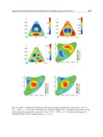
Figure 14 shows the atomic force microscope (AFM) surface images of the thin pentacene film
deposited on the interfacial layer. In the device showing high mobility, large and rigid
granular domains were observed, for example, in the case of B3PyMPM, B4PyMPM,
B2PyMPM, and BmPyPhB. On the other hand, small grains or amorphous-like surface were
observed, for example, in the case of Alq3, FIrpic, and so on. From these results, we concluded
that the mobility in the p-type hetero-layered OFETs composed of pentacene and electron
transporting material is determined by the structural effects rather than the energetic effects.
The material group of B3PyMPM, B4PyMPM, B2PyMPM, and BmPyPhB showed large grains
and higher mobility. These molecules were developed for electron transporting materials of
OLED devices and very high performance was achieved (Tanaka et al., 2007; Sasabe et al.,
2008). However, their LUMO levels are distributed from 3.71 eV (B4PyMPM) to 2.62 eV
(BmPyPhB). Therefore it is difficult to group these four materials by energetic properties, and
electron accepting character leading to charge transfer seems to be not concerned. One
plausible explanation is the molecular arrangement of the interfacial layer. These molecules
include nitrogen atoms in the benzene ring. Since nitrogen atom has higher electron affinity
that carbon atom, the nitrogen part become negatively charged. On the other hand, SiO2
surface without inert surface treatment has OH (hydroxyl) groups and its proton becomes
positively charged. Therefore the nitrogen atoms in these molecules are attracted to the weak
positive charge and the molecule would lie flat on the surface. This effect can be interpreted as
electrostatic interaction between two point charges (nitrogen - and hydrogen +), rather than
interaction between dipole moments between the molecule and hydroxyl group. In order to
159
Organic Field-Effect Transistors Using Hetero-Layered Structure with OLED Materials
maximize Coulomb stabilization, all the nitrogen atoms should touch the surface, resulting in
flat arrangement of the molecule on the surface. Consequently, very smooth and flat surface is
achieved and pentacene film is expected to form high crystalline film with large grains.
Bare
BP4mPy
0.282 cm2/Vs
BmPyPhB
0.276
B2PyMPM
Alq3
0.024
0.320
0.068
B4PyMPM
NTCDA
HAT(CN)6
0.388
0.193
0.033
TmPyPB
0.019
0.361
BCP
CBP
0.167
B3PyMPM
0.486
FIrpic
0.019
BTB
0.045
Fig. 14. AFM surface images of the pentacene film deposited on various interfacial layers.
δδ-
SiO2 surface
+
Hδ
O
Si
+
Hδ
O
Si
Fig. 15. Molecular arrangement model of B3PyMPM on the SiO2 surface.
Thus, the concept of heterolayered OFET was extended to p-type pentacene OFET with
electron transporting interfacial layer. The performance was slightly improved, but it was
mainly attributed to the effect of film structures. It was suggested that the electron transport
material including nitrogen atoms forms a preferable underlayer to improve the crystallinity
of the pentacene film on it.
5. Conclusion
In this chapter, we introduced a concept of heterolayered OFET composed of the channel
organic semiconductor layer and the interfacial organic semiconductor having opposite
polarity. In the HTL/n-type devices, the initial performance and stability in air was
significantly improved. This effect can be attributed to electron transfer from HTL to n-type
semiconductor at the interface, resulting in filling interfacial traps in advance. In the ETL/p-
160
Organic Light Emitting Diode – Material, Process and Devices
type devices, the performance was slightly improved, but that was mainly attributed to
structural effect of film formation.
The hetero-layered OFET is very simple method. The device can be fabricated only by
subsequent evaporation of two materials. It does not need self-assembly monolayer
treatment taking a long time. Furthermore, it can be expected to solve the most serious
problems in n-type OFET of mobility and stability in air. Our results suggest that air stable
OFET without designing a new material having deep LUMO level. We expect a novel
science and engineering for this “in-plane” carrier transport at the interface subjected to
electrostatic gradient.
6. Acknowledgement
This study was partially supported by the New Energy and Industrial Technology
Development Organization (NEDO), Precursory Research for Embryonic Science and
Technology (PRESTO) program of the Japan Science and Technology agency (JST), and
Grant-in-Aid for Scientific Research in Japan.
7. References
Chua, L. L., Zaumseil, J., Chang, J. F., Ou, E. C. W., Ho, P. K. H., Sirringhaus, H., and Friend,
R. H., (2005) General observation of n-type field-effect behaviour in organic
semiconductors, Nature Vol.434, No.7030, pp. 194-199, 193.
Dimitrakopoulos, C. D. and Malenfant, P. R. L., (2002) Organic thin film transistors for large
area electronics, Adv. Mater. Vol.14, No.2, pp. 99-+, 510.
Lim, S. C., Kim, S. H., Lee, J. H., Kim, M. K., Kim, D. J., and Zyung, T., (2005) Surface-treatment
effects on organic thin-film transistors, Synth. Met. Vol.148, No.1, pp. 75-79, 22.
Lin, Y. Y., Gundlach, D. J., Nelson, S. F., and Jackson, T. N., (1997) Stacked pentacene layer
organic thin-film transistors with improved characteristics, IEEE Electron Device
Lett. Vol.18, No.12, pp. 606-608, 189.
McCulloch, I., Heeney, M., Bailey, C., Genevicius, K., Macdonald, I., Shkunov, M., Sparrowe,
D., Tierney, S., Wagner, R., Zhang, W., Chabinyc, M. L., Kline, R. J., McGehee, M.
D., and Toney, M. F., (2006) Liquid-crystalline semiconducting polymers with high
charge-carrier mobility, Nat Mater Vol.5, No.4, pp. 328-333, 1476-1122.
Rost, C., (2004) Ambipolar organic field-effect transistor based on an organic
heterostructure, Vol.95, No.10, pp. 5782, 00218979.
Rost, C., Karg, S., Riess, W., Loi, M. A., Murgia, M., and Muccini, M., (2004) Ambipolar
light-emitting organic field-effect transistor, Vol.85, No.9, pp. 1613, 00036951.
Sasabe, H., Chiba, T., Su, S. J., Pu, Y. J., Nakayama, K., and Kido, J., (2008) 2Phenylpyrimidine skeleton-based electron-transport materials for extremely
efficient green organic light-emitting devices, Chem Commun (Camb) No.44, pp.
5821-5823, 1359-7345.
Singh, T. B., Sariciftci, N. S., Yang, H., Yang, L., Plochberger, B., and Sitter, H., (2007) Correlation
of crystalline and structural properties of C[sub 60] thin films grown at various
temperature with charge carrier mobility, Vol.90, No.21, pp. 213512, 00036951.
Tanaka, D., Sasabe, H., Li, Y.-J., Su, S.-J., Takeda, T., and Kido, J., (2007) Ultra High Efficiency
Green Organic Light-Emitting Devices, Vol.46, No.1, pp. L10-L12, 0021-4922 1347-4065.
Tatemichi, S., Ichikawa, M., Koyama, T., and Taniguchi, Y., (2006) High mobility n-type
thin-film transistors based on N,N '-ditridecyl perylene diimide with thermal
treatments, Appl. Phys. Lett. Vol.89, No.11, pp. 21.
6
Organic Light Emitting Diodes Based
on Novel Zn and Al Complexes
Petia Klimentova Petrova, Reni Lyubomirova Tomova
and Rumiana Toteva Stoycheva-Topalova
Institute of Optical Materials and Technologies “Acad. J. Malinowski”
Bulgarian Academy of Sciences
Up to 1 July 2010 Central Laboratory of Photoprocesses “Acad. J.Malinowski”
Bulgaria
1. Introduction
Organic light emitting diodes (OLEDs) have gained great interest in the last years due to
their potential for future flat panel display and solid state lighting applications. OLEDs are a
novel and very attractive class of solid-state light sources, which generate a diffuse, nonglaring illumination with high color rendering. Compared to the other major lighting
technologies in the market – incandescent, fluorescent, high intensity discharge (HID)
lamps, LED and electroluminescent, OLED technology has the potential of achieving
substantial energy and CO2 savings, without compromising color rendering or switching
speed. The unique features of OLED lighting are inspired the imagination of designers who
are exploring various OLED applications: windows, curtains, automotive light, decorative
lighting and wall papers. The OLED technology is now being commercialized as a multibillion dollar market. OLEDs are already used in small displays in cellular phones, car
stereos, digital cameras, etc. The rapidly growing market for OLED displays and lighting
is driving research in both advanced materials and improved manufacturing processes. In
spite of the spectacular results achieved, there are still many problems concerning the
efficiency, stability and lifetime of OLEDs, materials selection and optimization,
encapsulation, uniformity over large areas, manufacturing cost, colour saturation, etc. to
be solved.
OLED represents a quite complicated system of many very thin layers of various materials
situated between electrode layers (one of which is transparent); this system emits light when
placed under electric potential. The type of material used as the light emitter determines the
specific characteristics of such devices.
Two types of OLEDs are developed – on the bases of “small” molecules (SM-OLED) (Tang
& VanSlyke, 1987) and conjugated polymers (PLED) (Burroughes et al., 1990), oligomers,
etc. Potential emitters for SM-OLED are metal complexes from the lanthanide and platinum
groups as well as complexes of Al, Zn, Cd, Cu, Be, B with carefully selected ligands from the
group of heterocyclic compounds like as hydroxyquinoline, benzoxazole, benzothiazole,
triarylamines, etc. (Petrova & Tomova, 2009). The first generation of efficient devices,
pioneered by Tang and Van Slyke from Eastman Kodak (1987), was based on fluorescent
162
Organic Light Emitting Diode – Material, Process and Devices
materials. In this case, the emission of light is the result of the recombination of singlet
excitons, but the internal quantum efficiency is limited to 25%. The second generation uses
phosphorescent materials where all excitons can be converted into emissive triplet state
through efficient intersystem crossing (Baldo et al.,1998). Such materials are up to four times
more efficient than fluorescent materials.
An important aspect to improve OLEDs performances is suitable selection of materials for
functional OLED layers. In this work we have presented our successful decisions for all
functional layers – hole transporting, electron transporting, buffer, hole blocking,
electroluminescent in the structures of OLEDs. The new examined electroluminescent Zn
and Al complexes were synthesized in the Laboratory of Dyes Synthesis at the Department
of Applied Organic Chemistry, Faculty of Chemistry, Sofia University ”St. Kl. Ohridski”.
2. OLED structure
The simplest OLED structure is a single layer device architecture, where the organic emitter
is deposited between two electrodes and acts as emitter and as charge transport material
(holes and electrons) at the same time. If a forward bias voltage is applied to the electrodes
of an OLED device as depicted in Fig.1a, electrons from the cathode and holes from the
anode are injected into the organic semiconductor. The oppositely charged carriers move
towards each other across the organic semiconductor, encountere, recombine to form
excitons and some of them decay radiatively. The efficiency of an OLED is determined by
the number of charge carriers that are injected and the number of holes and electrons that
actually recombine during emission of light. In order to improve the device efficiency, the
multi layer OLED architecture was introduced (Fig.1b).
Nowadays devices may have a total of 7–9 layers of active materials: an anode; anode buffer
layer (ABL), hole injecting layer (HIL) or electron blocking layer (EBL); hole transporting
layer (HTL); emissive layer (EML); electron transporting layer (ETL) or hole blocking layer
(HBL), electron injecting layer (EIL); cathode buffer layer (CBL), a cathode and a protective
barrier layer (Tomova et al., 2007). Inserting of these layers facilitates charge carrier injection
by reducing the respective injection barriers; enhances the recombination of electrons and
holes in the emissive layer (due to accumulation of charges in the EL); shifts the
recombination area towards the middle of the device and thus prevents the quenching of the
excitons at the electrodes.
a)
b)
Fig. 1. Structure of: a) monolayer OLED; b) multilayer OLED.
Organic Light Emitting Diodes Based on Novel Zn and Al Complexes
163
The bilayer OLED consisting of hole transporting layer and emissive layer of different
electroluminescent “small” moleculear materials is a basic structure in our investigations.
They were prepared by thermal evaporation in vacuum better than 10-4 Pa at rates 2-5 A/s
on commercial polyethylene terеphtalate (PET) flexible substrate, coated with transparent
anode of In2O3:SnO2 (ITO - 40 Ω/sq). As cathode was used Al electrode, thermal evaporated
in the same vacuum cycle.
We studied the morphology, photoluminescence (PL), electroluminescence (EL) and the
performance of the devices measuring the current-voltage (I/V), luminescence-voltage
(L/V) and electroluminescence-voltage (EL/V) characteristics. The electroluminescent
efficiency (ηL) was calculated by equation (1) and used for quantifying the properties of the
OLEDs.
ηL = L / I
(1)
(where L is the luminescence (in cd/m2) and I is the current density (in A/m2) and used for
quantifying the properties of the OLEDs.
All measurements were carried out with unpackaged devices with area of 1cm2, at room
temperature and ambient conditions.
3. Hole transporting and buffer layers
The operating mechanisms of OLEDs involve injection of electrons and holes into the
organic emitter layers from the electrodes. During recombination, electrons and holes
generate molecular excitons (Kido et al., 1998), which result in the emission of light from the
emitter layer. Тherefore the effective recombination of electrons and holes affects on the
electroluminescence efficiency of organic light-emitting diodes. That’s why, it is important
to balance the number of holes and electrons in EL devices. The mobility of holes in OLED
materials used as the hole transport layer (HTL) is some orders of magnitude greater than
that of the electrons in the ETL (Zheng et al., 2005). The recombination zone is shifted
towards the cathode, which usually leads to a non-radiative loss of energy (Rothberg et al.,
1996) and decreasing of an OLED efficiency (Sheats et al., 1996). For that reason, by reducing
the mobility of holes in HTL or promoting electron injection into ETL can improve the
balance of carriers in OLED. The reducing of holes mobility can be achieved via inserting a
proper buffer layer between anode and hole transporting layer. On the other hand
introducing of a buffer layer improve the ITO morphology such as inhomogenity or
protrusions, impede the diffusion of indium into the organic layer during device operation,
which is correlated with the decay of a device’s performance (Schlatmann et al., 1996).
The ITO/organic interface morphology play a key role to stable operation and efficiency of
the device. For that reaseon, a lot of work has been devoted to the anode buffer layers
(ABLs) between ITO and the organic material. The introduced buffer layers mainly can be
divided in inorganic and organic compounds. Among the reported inorganic anodic buffer
layers good inorganic insulators such as transparent metal oxides Pr2O3, Y2O3, Tb4O7, ZnO
(Xu et al., 2001), Al2O3 (Li et al., 1997; Xu et al., 2001), SiO2 (Deng et al., 1999; Xu et al., 2001),
silicon nitride Si3N4 (Jiang et al., 2000; Xu et al., 2001), carbon nitride a-C:N (Reyes et al.,
2004), transition metal oxides, also V2O5, (Wu et al., 2007; Guo et al., 2005), MoOx (You et al.,
2007; Jiang et al., 2007), WO3, (Jiang et al., 2007; Meyer et al., 2007), CuOx, (Hu et al, 2002; Xu
et al., 2001), NiO, (Chan et al., 2004; Im et al., 2007) and Ta2O5 (Lu & Yokoyama, 2003), have
164
Organic Light Emitting Diode – Material, Process and Devices
attracted much attention due to their capability to lower the hole-injection barrier and
improve the interface morphology.
As the organic buffer layers a variety of materials as copper phthalocyanine (Van Slyke et
al., 1996; Shi & Tang, 1997; Tadayyon et al., 2004), α-Septithiophene (Park et al., 2002),
Langmuir-Blodjett
films
of
polymethylmethacrylate
(Kim
et
al.,
1996),
polytetrafluoroethylene (Gao et al., 2003), fluoropolymers (Wang et al., 2006), fluorenebased poly(iminoarylene)s (Jung et al., 2002), conductive polymer such as polythiophene
(Arai et al., 1997), poly(3,4-ethylenedioxythiophene) (Carter et al., 1997; Berntsen et al.,
1998), and polyaniline (Krag et al., 1996) etc. have been tested.
We explored the effect of p-isopropenylcalix[8]arenestyrene copolymer (iPrCS and
polycarbonate (PC), as buffer layers in OLED, and the incorporation of TPD with PVK as
hole transporting layer.
3.1 p-Isopropenylcalix[8]arenestyrene copolymer (iPrCS)
The calixarenes are a class of bowl-shaped cyclo-oligomeres obtained via phenolformaldehyde condensation with a defined upper and lower rim, and a cavity. This
speciality enable them to act as host molecules due to their cavities, and allow utilized them
as chemical sensors, extractants for radioactive waste processing, materials for non-linear
optics, bio-active compounds.
CH3
CH2
H3C
C
OH
OH OH
CH2
CH2
CH2
CH
CH2
CH2
m
z
6
C
C
CH2
CH3
Fig. 2. Chemical structure of the p-Isopropenylcalix[8]arenestyrene copolymer used in
device fabrication as buffer layer.
In this work, we offer the p-Isopropenylcalix[8]arenestyrene copolymer (iPrCS) as a novel
anode buffer layer (ABL) for the fabrication of OLED with improved efficiency and life time.
The p-Isopropenylcalix[8]arenestyrene copolymer (Fig.2) employed (Petrova et al., 2010) for
this study was for the first time synthesized according to described procedure (Miloshev &
Petrova, 2006), in University of Chemical Technology and Metallurgy, Sofia. Until now the
calix[4]arene compounds were used only for design of electroluminescent complexes - for
ex. a calix[4]arene [Al I]3+ complex (Legnani et al., 2004), lanthanide complexes with
calix[4]arene derivatives (Wei et al., 2007).
Two types of devices were investigated: ITO/ABL/TPD/Alq3/Al, and ITO/TPD/Alq3/Al
as a reference structure. The buffer layer (δ = 10 - 16 nm) of iPrCS was deposited on
PET/ITO substrates by spin-coating from 0.1 - 0.3% solution in THF at 2000 rpm. N, N’bis(3-methylphenyl)-N, N’-diphenylbenzidine (TPD) (δ = 30 nm) as hole transporting and
tris(8-hydroxyquinoline) aluminum (Alq3, δ = 50, 75 nm) as electroluminesent and electron
165
Organic Light Emitting Diodes Based on Novel Zn and Al Complexes
iPrCS (10 nm)/TPD/Alq3
iPrCS (13 nm)/TPD/Alq3
iPrCS (16 nm)/TPD/Alq3
TPD/Alq3
75
50
25
a
0
0
5
10
iPrCS (10 nm)/TPD/Alq3
2
100
Luminescence (cd/m )
2
Current Density (mA/cm )
transporting layer were used. TPD, Alq3 and the Al cathode (δ = 120 nm) were deposited via
thermal evaporation in a vacuum better than 10-4 Pa at rates of 2-5A/s.
Figure 3 presents typical nonlinear current/voltage (Fig.3a), luminescence/voltage (Fig.3b)
and efficiency characteristics (Fig.3c) of ITO/iPrCS (10-16nm)/TPD (30nm)/Alq3 (50nm)/Al and
ITO/TPD (30nm)/Alq3 (50nm)/Al as a reference structure. It was shown that the turn-on voltage
slightly decreased with increasing of the thickness of iPrCS, while the luminescence and
efficiency of devices increased and reached maximum values at a thickness of 13 nm. The
efficiency of 2 cd/A at 13 nm iPrCS was nearly 80% higher than those of 1.2 cd/A of the
reference structure.
15
20
iPrCS (13 nm)/TPD/Alq3
750
iPrCS (16 nm)/TPD/Alq3
TPD/Alq3
500
250
b
0
25
10
Electroluminescent
efficiency (cd/A)
Voltage (V)
15
20
Voltage (V)
25
iPrCS (10 nm)/TPD/Alq3
3
iPrCS (13 nm)/TPD/Alq3
iPrCS (16 nm)/TPD/Alq3
TPD/Alq3
2
1
c
0
0
25
50
2
Current Density (mA/cm )
Fig. 3. a) Current/voltage, b) luminescence/voltage and c) efficiency characteristics of
ITO/iPrCS/TPD (30nm)/Alq3 (50nm)/Al, and ITO/TPD (30nm)/Alq3 (50 nm)/Al.
Effect of the two thicknesses of Alq3 on the performance of the devices with 13 nm film
iPrCS is presented in Fig.4. It was established that the luminescence (Fig.4b) and efficiency
(Fig.4c) of the devices with iPrCS were higher compared to the reference structures and that
the device with 75 nm emissive layer of Alq3 showed the best characteristics. The efficiency
of 3.04 cd/A at the current density of 20 mA/cm2 of the device with iPrCS is similar to those
of 3.4 cd/A at the same current density, reported by Okamoto for the structure
ITO/CFx/NPB (60 nm)/Alq3 (60nm)/LiF/Al (Okamoto et al., 2006).