Photodiodes World Activities in 2011 Part 2 pot
Bạn đang xem bản rút gọn của tài liệu. Xem và tải ngay bản đầy đủ của tài liệu tại đây (1 MB, 30 trang )
An Absolute Radiometer Based on InP Photodiodes
21
H G. Bach, A. Beling, G. G. Mekonnen, and W. Schlaak,(2002).“Design and fabrication of
60-Gb/s InP-based monolithic photoreceiver OEICs and Modules”, IEEE J. Select.
Topics Quantum Electron., vol. 8,pp. 1445-1450, Nov./Dec. 2002.
R.Thomas Hawkins II, M. D. Jones,S. H. Pepper, and J. H. Goll, (1991).”Comparison of fast
photodetector response measurements by optical heterodyne and pulse response
techniques,” J. Lightwave Technol, vol. 9,pp. 1289–1294 , 1991.
S. Kawanashi, A. Takada, and M. Saruwatari,(1989). ” Wide-band frequency response
measurement of optical receivers using optical heterodyne detection,” J. Lightwave
Technol. , vol. 7, No. 1,pp. 92–98, Jan. 1989.
P. Debie and L. Martens,(1995).”Correction technique for on-chip modulation response
measurements of optoelectronic devicees,” IEEE trans. on Microwave Theory
Tech., vol. 43, no. 6, pp. 1264–1269, June 1995.
G. Unterborsch, A. Umbach, D. Trommer, G. G. Mekonnen,(1997).”70GHz long-wavelength
photodetector,” in Proc.28th Eur. Conf. on Opt. (ECOC ’97), pp. 25-28, Sep. 22–25
1997.
G.Wang, T. Tokumitsu,I. Hanawa, Y. Yoneda, K. Sato, and M. Kobayashi,(2003). ” A time-
delay equivalent-circuit model of ultrafast p-i-n photodiodes,” IEEE Trans. on
Microwave Tech., vol. 51, No. 4, pp. 1227–1233, April 2003.
A. Siefke, M. Dahlstrom, U. Westergren, X. J. Leijtens, N. van Melick, and M. K.
Smit,”Integration of an 8×10 GHz polarization independentWDMreceiver with
HBT-preamplifiers,” proc. symp. IEEE/LEOS Benelux Chapter,pp. 25–28,Gent,
Belgium.
A. Alping,” Waveguide pin photodetectors: theoritical analysis and design
criteria,(1989)procedins, vol. 136,Pt.J, No. 3, pp. 177–182, June 1989.
O.Wada, H.Hasegawa, K. Taguchi,(2002). “InP Based materials and devices” John Wiley,
ISBN: 0-471-18191-9. Unietd States of America.
J. Campos, P. Corredera, A. Pons, A. Corróns J. L. Fontecha.(1998). “Reflectance
dependencies of silicon trap detectors”. ,IOP Metrología, 35, 455-460.
P Corredera, M L Hernanz, M González-Herráez,J.Campos(2003). “Anomalous non-linear
behaviour of InGaAs photodiodes with overfilled illumination” IOP Metrología 40,
S181-S184.
P Corredera, M L Hernanz, J Campos, A Corróns, A Pons and J L Fontecha.(2000).
“Comparison between absolute thermal radiometers at wavelengths of 1300 nm
and 1550 nm” IOP Metrología. 37. 237-247.
J.Castrellon, G.Paez, M.Strojnik.(2002) “Radiometric analisis of a fiber optic temperatura
sensor” Opt. Eng, 41 (6),1255-1261.
R. Goebel, S. Yilmaz, R.Pello.(1996). “Polarization dependence of trap detectors” IOP
Metrología, 33,207-13.
E.F.Zalewski, C.R.Duda, “Silicon photodiode device with 100% external quantum
efficiency” Appl.Opt.,22, 2867-2873.
J.M.Coutin, F.Chandoul, J.Bastie. (2005).“Characterization of new trap detectors as transfer
standards” Proceedings of the 9th international conference on new developments
and applications in optical radiometry.
A.L.Muñoz Zurita, J.Campos Acosta, A.S.Shcherbakov, A.Pons Aglio.(2006).“Medida de
reflectancia y de fotodiodos de InGaAs/InP”. Proc. of the VIII National Meeting on
Optics, (Optical Society of Spain), p.27-30.
Photodiodes - World Activities in 2011
22
A.L.Muñoz Zurita, J.Campos Acosta, A.S.Shcherbakov, and A. Pons Aglio.(2007).
“Measuring the reflectance and internal quantum efficiency of InGaAs/InP
photodiodes in near infrared range”. Proc.of the IX International Congress on
Advanced Infrared Technology and Applications, (AITA-9), p.1-6.
A.L.Muñoz Zurita, J.Campos Acosta, A.Pons Aglio. A.S.Shcherbakov.(2007). “Medida de la
reflectancia de fotodiodos de InGaAs/InP” Óptica Pura y Aplicada, 40(1), 105-109.
A.L.Muñoz Zurita, J.Campos Acosta, A.S.Shcherbakov, and A.Pons Aglio.(2008) “Measuring
the reflectance and the internal quantum efficiency of silicon and InGaAs/InP
photodiodes in near infrared range”. Proc of SPIE Photonics West Conference
(January 22-26, 2008, San José, USA).
A.L.Muñoz Zurita, J.Campos Acosta, A.S.Shcherbakov, and A.Pons Aglio. (2008). “External
Quantum efficiency of some InGaAs/InP photodiodes”, Proc of NewRad2008
congress, MO_P41, (1-3).
2
Physical Principles of Photocurrent Generation
in Multi-Barrier Punch-Through-Structures
A.V. Karimov, D.M. Yodgorova and O.A. Abdulkhaev
Physical-Technical Institute of the Scientific Association
"Physics-Sun" of the Academy of Sciences
of the Republic of Uzbekistan, Tashkent
Uzbekistan
1. Introduction
The reach-through effect representing close up the space charge regions of two adjacent
oppositely biased junctions leads to a sharp exponential increase in current from the bias
voltage (Sze et al., 1971). Therefore, this effect was originally found in transistor structures
was undesirable. But in the further development of electronics, this effect has found many
applications in electronic devices. For example, in barrier injection transit-time diodes as dc-
current bias (Chu & Sze, 1973; Coleman & Sze, 1971; Presting et al., 1994), in static induction
transistors as an extra advantageous current to increase the transconductance of the
transistor (Nishizawa & Yamamoto, 1978), in low-voltage transient voltage suppressors as a
clamp device (de Cogan, 1977; King et al., 1996; Urresti et al., 2005), in JFET optical detectors
as a reset mechanism (Shannon & Lohstroh, 1974, as cited in Lohstroh et al., 1981), in IGFET
tetrodes as a modulated current flow (Richman, 1969, as cited in Lohstroh et al., 1981), in
punch-through insulated gate bipolar transistors (Iwamoto et al., 2002), in gate-field-
controlled barrier-injection transit-time transistors and in light injection-controlled punch-
through transistors (Esener & Lee, 1985).
Due to the predominance the diffusion processes in structures with reach-through effect
(Lohstroh et al., 1981; Sze et al., 1971) characters of the generation-recombination processes in
the space charge regions in these structures, as well as non-stationary processes caused by
extraction of the majority carriers and formation of the uncompensated space charge in the
base layer are still remain unexplored. To prevent the diffusion processes three-barrier
structure was developed, in which the flow of both types of carriers in the structure is limited
by rather high potential barriers (Karimov, 1991, 1994, 2002). This allowed us to research in
such structures the generation-recombination processes in the space charge regions after
reach-through, as well as the influence of illumination on these processes. In these structures is
found the internal photocurrent gain (Karimov & Karimova, 2003; Karimov & Yodgorova,
2010), which can not be associated with an avalanche or injection processes. Thus, this section
is devoted to disclosing the mechanisms of charge transport and the nature of the internal
photocurrent gain in multibarrier reach-through-photodiode structures.
In this section, is given a brief overview of multibarrier photodiode structures, as well as the
results of a comprehensive research of the dark and light characteristics of multibarrier reach-
through-photodiode structures. On the basis of which is proposed model, which explains the
mechanism of charge transport and internal photocurrent gain, as well as some future trends.
Photodiodes - World Activities in 2011
24
2. An overview of multibarrier photodiode structures
The sensitivity and the bandwidth of the photodetector is critical to the overall performance
of the receiver. A higher sensitivity translates into a longer distance possible between the
last repeater and the receiver, without loss of data. The bandwidth of the photodetector will
define the overall upper bandwidth limit of the receiver. There are two major types of the
photodetector used in the telecommunication systems today – a p-i-n photodiode and an
avalanche photodiode. The sensitivity of the p-i-n photodiode by itself is often too low for
long-haul applications, typically, as the bandwidth is increased, the sensitivity is decreased.
The alternative to the p-i-n photodiode, the avalanche photodiode, improves the sensitivity
of the p-i-n photodiode by an additional section of the chip (section with high enough
electric field for the formation of the avalanche multiplication) that provides gain.
Depending on the gain of the device the sensitivity can be varied over a few dB without
severe penalty in the bandwidth of the device. However, there is an additional noise
associated with the gain section of the device which will impact receiver sensitivity. Also, at
high gains, the device bandwidth will be limited by the gain-bandwidth product (a typical
value of this product is 100 GHz). A typical operating current gain of the gain section of the
device is 3 to 10 without penalty in the device bandwidth. In this rang the device is usually
RC-limited. One of the first multibarrier structures with internal photocurrent gain is a
bipolar phototransistor (Campbell, 1982). A phototransistor can have high gain through the
internal bipolar-transistor action, which was significantly improved by utilizing a wide-gap
emitter (Chand et al., 1985), or by utilizing punch-through transistors (Esener & Lee, 1985).
It should be noted that the inherent to transistors large areas degrades their high-frequency
performance.
Semiconductor device with two metal-semiconductor rectifying junctions can also be
attributed to multibarrier photodiode structures (Sugeta & Urisu, 1979). In these structures,
high performance is ensured by non injecting metal-semiconductor junctions and low
capacitance of planar barriers. Non injecting nature of the metal-semiconductor junction
suppresses internal photocurrent gain. Presence of the carrier injection in one of the
junctions allowed one to obtain photocurrent gain for low-frequency range. Internal
photocurrent gain in the high-frequencies has been achieved only when avalanche
multiplication is present. However, in case of variation of the parameters of the potential
barriers may cause some amplification of the primary photocurrent. The mechanism of the
observed internal photocurrent gain can be attributed to the formation of a nonuniform
electric field distribution and the separation of light-generated carriers near the anode with
simultaneous additional emission of electrons from the cathode (Klingenstein et al., 1994).
However, the use of series-connected heterojunctions and metal-semiconductor junctions
allows one to control the spectral range of responsivity.
Series connection of the three barriers to longer enough short base layers allows one to
obtain the internal photocurrent gain as a photothyristor. However, it is having the S-
shaped current-voltage characteristic leads to instability of its parameters, and therefore can
only be used as an optical switch. By serial connection of the p-n-junction with a high
resistive long-base layer were obtained the injection-based photodiodes whose
characteristics are similar to photothyristor characteristics (Vikulin et al., 2008). At the same
time these photodiodes are had sufficient internal gain in the prebreakdown region, but
decreased high-frequency performance.
Thus, in most multibarrier photodiode structures are inconsistent the high-frequency
performance and the photosensitivity, i. e. there is a competitive relationship between them,
which leads to the constancy of their product. In this aspect, it would be appropriate to
Physical Principles of Photocurrent Generation in Multi-Barrier Punch-Through-Structures
25
create a new class of multibarrier photodiode structures that is an alternative to avalanche
photodiodes and field phototransistors.
3. Three-barrier reach-through-photodiode structure
Investigated a three-barrier reach-through-photodiode structures on basis of gallium
arsenide were produced on base of technology for obtaining abrupt p-n-junctions from
epitaxial homolayer or heterolayer p(n)-type which was growth from a liquid phase on
substrate n(p)-type (we used a substrates doped with shallow or deep impurities). The
carrier concentration in the grown epi-layer (with thickness 1-2 microns) was 5-7·10
15
cm
-3
and in the substrate 1-9·10
15
cm
-3
. By evaporation in a vacuum of the translucent layers Ag
(70 Å) on both surfaces of structure were obtained rectifying junctions (in some samples to
obtain the barrier was used Au). Height of potential barriers were measured by a
photoelectric method are 0.6-0.8 eV and are determined by fixing the Fermi level on surface
states. As a result, were made three barrier m
1
-p-n-m
2
-structures with an area of 2-25 mm
2
,
in which m
1
-p- and n-m
2
-junctions are physically connected in series, and p-n-junction
opposite. Due to the existence of a blocking junction at any bias polarity these structures are
able to operate at both polarities of the bias voltage and a double-sided sensitive, i. e., the
photocurrent can be taken under illumination from either side of structure. The total
capacitance of the structure is close to the value determined by the geometric size of the
entire structure and is about 0.2-0.5 pF/mm
2
.
The proposed structure is similar to a thyristor, but differs from it in the larger thickness of
one of the base regions (the thickness of the n-region is equal to 350 microns), while in the
thyristor three barriers are separated by two base regions with a thickness, which is in one
order with the diffusion length of minority carriers (Sze & Kwok, 2007). In this case, the
smaller thickness of other base region contributes to close up the space charge regions of
adjacent junctions before the onset of avalanche multiplication.
4. The dark characteristics
Investigated m
1
-p-n-m
2
-structure in the initial bias voltages has typical current-voltage
characteristics for a structure with three successively connected barriers (i. e. the current
transport is determined by the reverse-biased junctions and in the case of the generation
mechanism the dependence is a power law with an index equal to 0.5), which are then in
voltages above a certain voltage (U
o
) changed to a linear dependence as resistors, Fig. 1. In
this case, the resistance was determined from the slope of current-voltage characteristics is
several orders of magnitude higher than determined by resistivity and the geometric sizes of
the base regions, which indicates the existence of potential barriers in the modified
structure. However, the observed linear character of current-voltage dependence can not be
explained within the existing theories of the barriers.
The observed behaviors of the current-voltage characteristics are associated with the effects
taking place in a three-barrier structure when the voltage is increased beyond the reach-
through voltage. As is well known for reach-through-structures charge transport through
these structures is determined by the minority carriers (in our case electrons) that are
emerging from the forward-biased junction. However, in the m
1
-p-n-m
2
-structure the metal-
semiconductor barriers restrict the flow of these carriers. Thus, in a three-barrier reach-
through-structures the current density through the structure after the reach-through is
determined by double-sided thermal electron emission, i. e. the flow of holes is limited by
the left barrier, while the flow of electrons is limited by the right barrier.
Photodiodes - World Activities in 2011
26
Fig. 1. Measured I-V characteristics of the three barrier structure at opposite bias polarities:
1 - (+)m-p-n-m(-); 2 - (-)m-p-n-m(+); γ – power index in I ~ V
γ
.
In case of forward biased p-n-junction in the initial bias voltages the space charge regions of
the metal-p and p-n-junctions are closed up which is caused by sufficiently thin base-layer.
In the further increase of bias voltage the energy bands of the p-n-junction tend to become
flat, which leads to a significant increase in current density of electrons from the n-region,
Fig. 2. According to the research (Sze et al., 1971), the current density of electrons from the
n-region is defined by:
2
*2
exp
4
pn
FB
nn
FB
qV V
jAT
kTV
(1)
It should be noted that the current density of electrons incoming to the n-region is limited by
the potential barrier of the n-metal-junction:
*2
exp
mn
mn
nn
q
jAT
kT
(2)
Therefore, in the n-region adjacent to the p-n-junction there is a strong depletion of the
major carriers, which leads to the formation of an uncompensated positive space charge of
ionized donors, which in turn attracts electrons from the nearby area leading to the
formation of new uncompensated positive space charges, which contributes to the further
development of non-stationary processes in n-region. These processes will continue until the
establishment of equilibrium between the currents of electrons emerging from the n-region
and incoming to the n-region. The required reduction in current density of electrons
emerging from the n-region is given by the decreasing of equilibrium concentration of
electrons in the n-region, which, while maintaining electrical neutrality of structure becomes
possible when the donors go to the neutral state. The conductivity of the n-region becomes
close to intrinsic conductivity, which leads to an increase in its resistivity and an increase in
the incident in this area bias voltage. As a result, the current-voltage characteristic of the
structure becomes close to linear. The degree of depletion of the n-region and thus its
resistivity determines by the current density of electrons through the n-metal junction:
Physical Principles of Photocurrent Generation in Multi-Barrier Punch-Through-Structures
27
mn
nregion n
Rfj
(3)
In case of reverse biased p-n-junction in the initial part of the current-voltage characteristics
the dependence is a power law with an index equal to 0.5, which is due to the predominance
of the generation processes in the space charge region of reverse biased junction. Above a
reach-through voltage the energy bands of the metal-p-junction tend to become flat, which
leads to a significant increase in current density of holess from the p-region, which leads to
the formation of an uncompensated negative space charge of ionized acceptors. Field of
space charge reduces the built-in potential of the n-metal-junction, leading to an increase in
Fig. 2. Energy band diagram of a three barrier structure at bias polarity (+)m-p-n-m(-) after
reach-through.
current density of electrons overcoming the barrier of n-metal while the current density of
electrons incoming to the n-region is limited by barrier metal-p. As a result, just as in the
above case, we have depleted n-region. Thus, the current-voltage characteristic of the
structure is changed to a linear one. The degree of depletion of the n-region and thus its
resistivity in this case are determined by current density of electrons through a metal-p:
m
p
nregion n
Rfj
(4)
Thus, for both polarities the current transport is determined by an identical mechanism. Due
to the fact that the barrier height of metal-p-junction is greater than the barrier of n-metal-
junction resistance of the structure in the mode of blocking of the p-n-junction is of greater
than another mode.
Temperature dependence of the resistance of the structure in the linear region in both modes
is described by the function (Fig. 3.)
1
exp( ( ))
C
RT f
T
(5)
As noted above the current flowing through the structure is determined by the resistance of
the depleted n-region, which in turn depends on the intrinsic carrier concentration in this
Photodiodes - World Activities in 2011
28
region and current density of electrons through the n-metal- (or metal-p-) junction, which
explains the existence of two linear regions with different slopes in this relationship.
Activation energy determined from these slopes at low temperatures corresponds to the
energy band gap, and at high temperatures to the potential barrier’s height. Accordingly,
the change in slope with increasing the temperature is caused by prevalence of the
thermionic electron current through the metal-semiconductor junction for high
temperatures.
Fig. 3. The resistance of the three barrier structure as a function of temperature at opposite
bias polarities in linear region of I-V characteristics: 1 - (+)m-p-n-m(-); 2 - (-)m-p-n-m(+)
Temperature coefficient of voltage break point of the current-voltage characteristic has a
negative value with a coefficient of -0.098 V/K, so we can assume that the break point is
uniquely determined by the reach-through of adjacent junctions of the structure.
Thus, despite the fact that the structure contains a number of series-connected barriers at
voltages higher than a reach-through voltage its current-voltage characteristic becomes
linear.
5. Light characteristics
Consideration of the structures in the photovoltaic mode, showed that in structure is
generated the photo-EMF. The dependence of short circuit current on the intensity of light is
nearly linear. Load characteristics in accordance with the current-voltage characteristics are
linear, which leads to increased half-width of the maximum output power.
Light characteristics taken from the integral lighting (incandescent lamp) at 100 lux are
shown in Fig. 4. In this figure solid line represents the data of the reference photodiode
(single-barrier p-n-photodiode) without internal gain. For the researched structures at both
polarities of the bias the photocurrent increases with bias voltage to much greater values
than in the reference photodiode indicating the presence of internal photoelectric gain. In
the reverse-biased p-n-junction at low voltages is taken a tendency to saturation of the
photocurrent, as in conventional photodiode without amplification, but when the voltage is
increased beyond the reach-through voltage the photocurrent begins steady with voltage.
Curves of light characteristics in case of forward-biased p-n-junction under illumination by
side of the p-type layer with increasing light intensity move in parallel toward higher
Physical Principles of Photocurrent Generation in Multi-Barrier Punch-Through-Structures
29
currents. This can be explained by the fact that from the light emission increases the current
density of electrons to the depleted n-region through the n-metal-junction, which leads to a
decrease in the degree of depletion and resistance of this region
mn mn mn
nre
g
ion n dark
p
hoto
Rfjfjj
(6)
Fig. 4. Photocurrents of the three barrier structure and reference photodiode as a function of
bias voltage at opposite bias polarities: 1 - (+)m-p-n-m(-); 2 - (-)m-p-n-m(+)
It is known that the light with energy in the region
g
hE
, which is absorbed in the
metal and excites photoemission of electrons from this metal is not absorbed in the bulk of
the semiconductor, so changing the illuminated area does not affect the sensitivity of the
photodiode.
Analysis of the spectral response of the three-barrier reach-throuch-structure (Fig. 5.) shows
that in the both polarities of the bias and regardless from the illuminated surface (top or
bottom surface) the photosensitivity is higher when the absorbed light excites
photoemission of electrons from the metal than the case when the absorbed light excites
intrinsic photogeneration. This agrees well above given mechanism of photosensitivity and
due to the fact that the resistance of the depleted n-region is determined only by the current
density through the metal-semiconductor junction.
It should be noted that in all the structures external quantum efficiency was greater than
unity and indicates the presence of internal gain in these structures. In this case, the
observed internal photocurrent gain in the structures does not fit into the framework of the
avalanche and the transistor (injection) effects.
6. Mechanism of the internal photocurrent gain
The mechanism of charge transport, depending on the polarity of the operating voltage
practically does not differ, which leads to the identity of the internal photocurrent gain in
both modes, so we restrict ourselves to the case for direct mode, i. e. forward-biased p-n-
junction mode.
Photodiodes - World Activities in 2011
30
In the forward-bias p-n-junction mode because of the narrowness of the p-region metal-p
junction and p-n-junction interlock quickly, which leads to an exponential increase in
current density of electrons from the n-region with the approach of the bias voltage to flat-
band voltage. In this case, the current density in the n-region is limited to the saturation
current density of n-metal junction. Since
pn
mn
nn
jj
, the n-region is depleted of electrons,
which leads to an increase in resistance of this region. Depletion of electrons continues until
the current density of electrons emerging from the n-region decreases did not reach a
current density of electrons incoming to the n-region. Thus, the degree of depletion is
determined by current density of electrons incoming to the n-region.
a) b)
Fig. 5. Spectral response of the three barrier structure at opposite bias polarities and
different bias voltages: а) (+)m-p-n-m(-); b) (-)m-p-n-m(+)
Thus, the structure represents a resistance whose value is controlled by a current density of
n-metal junction, that is, by nature, similar to the FET, but is controlled by current density.
Due to the fact that the intensity of light radiation directly controls the current density,
which in turn controls the resistance of the structure, this structure has the internal
photoelectric gain.
7. Structures with a heterojunction
Performing a three-barrier photodiode structure based heterojunction allows one to control
its spectral respons: take a selective sensitivity or enhance the optical range, in the long or
short waves. Increasing energy band gap of the base region can cover the short-wave part of
the spectrum, while reducing the energy band gap of p-type region can reduce the
sensitivity to shorter wavelengths until the completion of the selective sensitivity is
determined by the potential barrier of n-metal. Reducing the potential barrier height of n-
metal can expand the optical range to longer wavelengths.
Physical Principles of Photocurrent Generation in Multi-Barrier Punch-Through-Structures
31
In the case of a three-barrier photodiode Au-nAl
0.1
Ga
0.9
As-pGaAs-Ag-structure of the
current transport mechanism similar to the mechanism of homojunction structure, with the
difference that on case of reverse biased n-p-heterojunction with increasing voltage the
current dependence is changed from the linear to quadratic, which can be explained by the
mechanism of space-charge-limited current transport mechanism. Therefore, in this mode
include not observed internal photocurrent gain. However, in a case of forward biased
heterojunction the structure has the internal photoelectric gain (Fig. 6.), the magnitude of
which increases with both increasing the operating voltage and intensity of light. The
dependence of photocurrent on light intensity becomes superlinear character.
Spectral characteristics have also shown that the quantum efficiency in a direct displacement
of n-p-heterojunction regardless of the surface to be illuminated in a broad spectral range
from 0.95 to 1.3 eV (0.8 to 1.6 microns) unchanged, Fig. 7. By increasing the applied voltage
to 65 volts at a radiation power of 0.2 mW/cm
2
, the quantum efficiency of the structure
increases to 2.77, i. e. there is an internal photoelectric gain.
Fig. 6. Photocurrent of the three barrier structure with heterojunction as a function of bias
voltage
As noted above, in the structures long base region is depleted of majority carriers and the
impurity goes into a neutral state. To verify this situation have been investigated with the
basic structure of the area containing deep impurity levels of oxygen. In this case, the
compositions heterolayers and metals were chosen so that the height of the barriers have
similar values and do not affect the current transport mechanism, and allowed us to
determine the influence of deep impurity. In Au-pAl
0.05
Ga
0.9
In
0.05
As-nGaAs:O-Ag-structure
for both polarities of bias the current-voltage characteristics, spectral response and
capacitance-voltage characteristics were identical. Spectral characteristics when excited by
heterolayer show that the maximum photocurrent due to excitation of carriers from metal
with a characteristic tail of the excitation of carriers from deep levels of oxygen, Fig. 8.
Raising the temperature leads to a broadening of the spectral characteristics of a clear
manifestation of the photocurrent in the impurity region of the spectrum caused by oxygen
levels (Fig. 9.), and for a given temperature increase of confining the illuminated metal-
semiconductor junction bias voltage leads to a simultaneous increase in the photocurrent
spectrum in the whole range with simultaneous spectral broadening.
Photodiodes - World Activities in 2011
32
Fig. 7. Spectral response of the three barrier structure with heterojunction at different bias
voltages and in bias polarity (+)m-p-n-m(-)
Fig. 8. Normalized spectral response of the three barrier structure with deep impurity levels
of oxygen at different bias voltages and in bias polarity (+)m-p-n-m(-)
8. Some perspectives of multibarrier photodiode structures
Multibarrier photodiode structure with an appropriate choice of design parameters may
provide a basis to create new structures with improved properties that are of interest for
micro and optoelectronics.
Low-capacitance current-controlled transistor can be created can be created by forming a
planar rectifying and ohmic contacts to the surface of a thick n-type region of the m
1
-p-n-
structure. The result will be m
1
-p-n-m
2
-structure with an ohmic contact to the base n-type
region. Capacitance of the structure will be determined by the geometric dimensions of the
structure. It creates a voltage forward bias p-n-junction is applied to the electrodes of the
Physical Principles of Photocurrent Generation in Multi-Barrier Punch-Through-Structures
33
potential barriers, and input to the ohmic contact and the contact potential barrier. By
analogy with the field-effect transistor contact potential barrier, one might say, carry out the
role of the drain and source, an ohmic contact – the role of the gate. However, in contrast to
the FET output characteristics are controlled by the current of the gate. In the absence of the
input signal through the structure is minimal and determined by the resistance base and
lockable metal-semiconductor interface.
Fig. 9. Normalized spectral response of the three barrier structure with deep impurity levels
of oxygen at different temperatures and in bias polarity (+)m-p-n-m(-) at 2 V.
Small change in the gate current, i.e. in the current flowing through the barrier n-m
2
leads to
a stronger change in the total current through the structure. At the same time the output
characteristics are obtained with characteristics similar to the static induction transistor.
In another embodiment, instead of the potential barrier is proposed to form a semiconductor
n-p-junction. As a result multibarrier photodiode will be an m
1
-p-n-p structure with an
ohmic contact to n-base. The operating mode will create a voltage applied to the contacts of
the barrier and the p-contact area. Useful signal will be fed to the resistance connected to the
base and the p-region, or as a signal required for the gain can be a light signal fed to the n-p-
junction, where you will create short-circuit current is proportional to the intensity of the
radiation. As a result, the output is the amplified signal, ie, the proposed structure will have
multibarrier reinforcing properties.
Highly sensitive photodetector can be created by the serial connection m-p-n-structure to p-
n-junction. The result is a four barrier m-p-n-p-n-structure including a three-barrier m-p-n-p
and bipolar n-p-n-structure. Operating voltage is applied to the external contacts m
1
and n-
type region with a positive polarity to the contact potential barrier. In the dark current
through the structure is determined by the electronic component of the collector p-n-
junction, where the electrons have a significant barrier. Under illumination of the collector
junction is created that matches the sign of the photocurrent to the dark current and
summed. Coefficient of internal photoelectric amplification will consist of works of the gain
on the part of a three-barrier transistor gain.
Photodiodes - World Activities in 2011
34
Multibarrier photodiode structures are sensitive to impurity and intrinsic emission can be
created by the formation of a nonuniform distribution of deep impurities in a long base n-
region in m-p-n-structure. The structure is a thin stripe of p and a thick n-type lightly doped
layer (300 microns), which create internal barriers without illumination, did not exceed a
few kT. However, if covering own light barrier height can prevail kT, leading to a reduction
in current through the structure. When excited by light in the impurity region through the
structure will increase.
9. Conclusion
In multibarrier mpnm-photodiode structures with the effect of closure of adjacent
oppositely biased junctions, the mechanism of charge transport is determined by the
depletion of the major carriers in the base, leading to the development of transitional
processes in n-type region with the subsequent transition to a neutral donor state. The
degree of depletion n-region and its specific resistance are determined by current density of
electrons emerging from semiconductor-metal junction; the dependence of current on
voltage obeys a power law with an exponent close to unity and is due by the day the main
part of the external voltage on the depleted n-region.
Determining the noise and frequency properties of photodiode structures low capacitance
and dark current distinguishes multibarrier structure compared with other types of
detectors.
Performing a three-barrier photodiode structure based heterojunction allows you to control
its spectral range, a selective sensitivity and enhance the optical range, in the long or short
waves. Reducing the height of the barrier metal-semiconductor optical range can be
extended to longer wavelengths.
In multibarrier photodiode structures of the internal photoelectric amplification controlled
operating voltage and an order of magnitude more sensitive unijunction diode photodiode.
For their work does not require any cooling at room temperature provides the required
operating modes defined spectral regions (0.9 microns, 1.3 microns, 1.5 microns) with low
values of capacitance of the order 0,2-0.5 pF/mm
2
. In this case, the dark current for a voltage
of 100 V was 40-100 nA. Internal photoelectric amplification of photocurrent is provided
from the outset the applied voltage, ie, they possess sufficient sensitivity to record from low
supply voltages (5 V). Due to the high input resistance are easily switched with the field-
effect transistors and integrated circuits.
Thus, in the above material is presented original experimental data on the principles of
creating improved multibarrier photodiode structures, some features of their photoelectric
characteristics when exposed to light and heat radiation, the results of the analysis of
processes of charge transport and photocurrent gain.
10. References
Campbell, J. C. (1985). Phototransistors for lightwave communications. Semiconductors and
Semimetals,
Vol.22D, p. 389-447.
Chand, N.; Houston, P.A. & Robson, P.N. (1985). Gain of a heterojunction bipolar
phototransistor.
IEEE Transactions on Electron Devices, Vol.32, No.3, p. 622-627.
Physical Principles of Photocurrent Generation in Multi-Barrier Punch-Through-Structures
35
Chu, J. L. & Sze, S. M. (1973). Microwave Oscillation in pnp Reach-Through BARITT Diodes.
Solid-State Electronics, Vol.16, pp. 85.
Coleman, D. J., Jr. & Sze, S. M. (1971). A Low-Noise Metal-Semiconductor-Metal (MSM)
Microwave Oscillator.
Bell Syst. Tech. J., Vol.50, pp. 1695.
de Cogan, D. (1977). The punchthrough diode.
Microelectronics, Vol.8, No.2, pp. 20-23.
Esener, S. & Lee, S. H. (1985). Punch‐through current under diffusion-limited
injection: analysis and applications.
Journal of Applied Physics, Vol.58, No.3,
pp. 1380-1387.
Iwamoto, H.; Haruguchi, H.; Tomomatsu, Y.; Donlon, J. F. & Motto, E. R. (2002). A new
punch-through IGBT having a new n-buffer layer.
IEEE Transactions on Industry
Applications,
Vol.38, No.1, pp. 168-174.
Karimov, A. V. (1991). Karimov
s three-barrier photodiode. USSR Patent,
No.1676399.08.05.
Karimov, A. V. (1994). Karimov
s three-barrier photodiode. Uzb Patent, No.933.15.04.
Karimov, A. V. (2002). Three-barrier photodiode structure. 15 International Workshop on
Сhallenges in Predictive Process simulation,
рp. 71-72. Prague, Czech Republic, 13-17
October.
Karimov, A. V. & Karimova, D. A. (2003). Three-junction Au/AlGaAs(n)/GaAs(p)/Ag
photodiode.
Materials Science in Semiconductor Processing, Vol.6, No.1-3, pp. 137-
142.
Karimov, A. V. & Yodgorova, D. M. (2010). Some features of photocurrent generation in
single- and multibarrier photodiode structures.
Semiconductors, Vol.44, No.5, pp.
647-652.
King, Y.; Yu, B.; Pohlman, J. & Hu, Ch. (1996). Punchthrough diode as the transient voltage
suppressor for low-voltage electronics.
IEEE Transactions on Electron Devices, Vol.43,
No.11, pp. 2037-2040.
Klingenstein, M.; Kuhl, J.; Rosenzweig, J.; Moglestue, C.; Hülsmann, A.; Schneider, Jo. &
Köhler, K. (1994). Photocurrent gain mechanisms in metal-semiconductor-metal
photodetectors.
Solis-State Electronics, Vol.37, No.2, pp. 333-340.
Lohstroh, J.; Koomen, J. J. M.; Van Zanten, A.T. & Salters, R. H. W. (1981). Punch-through
currents in P+NP+ and N+PN+ sandwich structures—I: Introduction and basic
calculations.
Solis-State Electronics, Vol.24, No.9, pp. 805-814.
Nishizawa, J. & Yamamoto, K. (1978). High-frequency high-power static induction
transistor.
IEEE Transactions on Electron Devices, Vol.25, No.3, pp. 314-322.
Presting, H.; Luy, J F.; Schäffler, F. & Puchinger, J. (1994). Silicon Ka band low-noise
BARITT diodes for radar system applications grown by MBE.
Solid-State Electronics,
Vol.37, pp. 1599.
Sze, S. M.; Coleman, D. J. & Loya, A. (1971). Current Transport in Metal-Semiconductor-
Metal (MSM) Structures.
Solid-State Electronics, Vol.14, pp. 1209.
Sze, S. M. & Kwok, K. Ng. (2007). Physics of Semiconductor Devices. John Wiley & Sons,
Inc., Hoboken, New Jersey.
Sugeta, T. & Urisu, T. (1979). High-Gain Metal-Semiconductor-Metal Photodetectors for
High-Speed Optoelectronics Circuits.
IEEE Trans. Electron Dev., Vol.26, pp.
1855.
Photodiodes - World Activities in 2011
36
Urresti, J.; Hidalgo, S.; Flores, D.; Roig, J.; Rebollo, J. & Mazarredo, I. (2005). A quasi-
analyticl breakdown voltage model in four-layer punch-through TVS devices.
Solis-
State Electronics
, Vol.49, No.8, pp. 1309-1313.
Vikulin, I. M.; Kurmashev, Sh. D. & Stafeev, V. I. (2008). Injection-based photodetectors.
Semiconductors, Vol.42, No.1, pp. 112-127.
3
Photon Emitting, Absorption and
Reconstruction of Photons
Changjun Liao, Zhengjun Wei and Jindong Wang
University Laboratory of Guangdong, School for Information
and Optoelectronic Science and Engineering
South China Normal University, Guangzhou
China
1. Introduction
Photon cannot keep itself unchanged from emission to absorption. The information encoded
on the photon is also changed due to interaction with environments. There has no definitely
demonstration that the photon absorbed is the original one from ideal light source since the
quantum mechanics itself is an indeterminate theory that the physical measurement is only
the probability. Any operation on photon before detector involves unavoidably loss that
means a quantum permutation with environments. Although a photon is detected with
same energy the phase uncertainty exists. Section 2 describes the single photon sources and
the questions about the conception of photons. The third section describes the quantization
of electromagetic fields that makes the basis of the Fork states in that the number of the
photon is considered. In Section 4, the representation of the photon in space is described by
a complete set of eigenfunctions which represent the fundamental modes with different
eigen values. Concept of optical modes is a result of quantization of electromagnetic fields.
Optical modes can be occupied by photons in different way in comparison with levels in
atomic system in which Coulomb interaction considered. Bunching and anti-bunching are
considered as the fundamental properties of the optical modes in Section 5. Based on these
theories, several applications are considered. Directional emission of single photons is
considered in Section 6, study on single photon detectors is presented in Section 7,
multipartite entanglement and its application in quantum key distribution is introduced in
Section 8. The fluctuation in vacuum, dephase and decoherent are considered in Section 9.
General consideration of reconstructions of photons including coherent combination and
interfere coherently, resonant-enhanced density of photons are put in the last Section. Here
in this chapter photons are considered as field quantum theory instead of that quantum field
theory. Photons consist of mode fields which are quantized.
2. Sources of single photons
The concept of Photon has important contribution to the foundation of quantum mechanics
which can be seen in any textbook of quantum mechanics (Greiner, 2001). The "particles" of
light are called quanta of light or photons which are recognized to have wave-particle
duality, a typical feature of a quantum system. The concept of photon was soon
Photodiodes - World Activities in 2011
38
demonstrated by photoelectric effect. This effect was interpreted by Einstein with his
famous formula
aa
Eh
(1)
where E is a discrete quanta of light with energy of
, the Planck's constant 2h . The
quantized energy was soon demonstrated with many experiments, including the Compton
effects, the Ritz Combination principle, the Franck-Hertz experiment, etc.
Photons are ideal for quantum information applications due to its high transmission speed
and easy to be coded with quantum information.
Single photons and entangled photon pairs are important for quantum information. Single
photons are usually used in quantum key distribution (QKD) system as quantum
information carriers to ensure the security of a key distribution system based on quantum
mechanics principles (Gisin et al., 2002). The quantum mechanics assured that a single
photon can not be divided and a single photon can not be cloned either (Wootters & Zurek,
1982). Furthermore, a single measurement is not enough for determining the quantum state
with certainty, any measurement provides only the probability if the state is unknown and
the original state changed after measurement and can never be recovered again. Therefore
study on generation and detection of single photons is extremely important.
Light sources are everywhere. But real single photon sources are facing technical challenges.
Among many methods to provide single photons, three kinds of single photon sources have
attracted much attention: the faint optical pulses, spontaneous down conversion photon
pairs and quantum dot.
2.1 Faint laser pulses
In practice, the single photons are usually produced by precisely controlled attenuation of
laser pulses to a very weak level and assume at that level the photon follow Poisson
distribution.
!
n
n
Pe
n
(2)
where,
n
P
are the probability of the pulse containing n photons with mean photon number
of
(Walls & Milburn, 1994). The probability of containing more than one photon in faint
pulses can be made arbitrarily small. For example, with mean photon number of 0.1 as quite
usual, there is only 5% of the nonempty pulses contain photons more than one, most of the
nonempty pulses contain only single photon. These single photon sources are pseudo-
single-photons or correctly called faint laser pulses.
2.2 Down-conversion photon pairs
Single photon generators using correlated photon pairs generated by the spontaneous
parametric down-conversion are widely reported (Mason et al., 2002; Migdall et al., 2002;
Pittman et al., 2002; Walton et al., 2001). In particular, a periodically poled lithium niobate
waveguide has high probability for generation of photon pairs at 1550 nm (Tanzilli et al.,
2001; Yoshizawa et al., 2003; Mori et al., 2004). A photon pairs includes a signal photon and
an idler photon correlated in time. Therefore the detection of idler photon can be used to
control an optical switch so that the signal photon can surely emit in time. However, the
Photon Emitting, Absorption and Reconstruction of Photons
39
number distribution of the photon pairs follows also Poissonian statistics. A photon number
resolving detector is needed for idler photon if single photon emitting should be guaranteed
as required in quantum information applications. Photon number resolving detection faces
also technical challenges although several kinds of photon number resolving detectors have
been reported, they still far from commercially available (Kardyna et al., 2007; Miller et al.,
2003).
2.3 Single quantum dot emission
In theoretical consideration, single photons should come from a single transition between
two single state levels by one electron in single quantum cavity, such as single atom,
quantum dot, etc. It might be properly called "turn style" or "photon gun".
A single photon generation using semiconductor quantum dot has been reported (Santori et
al., 2001). Electrically driven single-photon source has been demonstrated experimentally
(Zhiliang Yuan et al., 2002). In their experiments, at low injection currents, the dot
electroluminescence spectrum reveals a single sharp line due to single exciton
recombination (one electron and one hole within a quantum dot), while another line due to
the biexciton emerges at higher currents. The second order correlation function of the diode
demonstrated anti-bunching under a continuous drive current with Hanbury-Brown and
Twiss arrangement (Hanbury-Brown & Twiss, 1956). But the efficiency of collecting the
emitted photons is low since the emission from single point diverges in all directions. The
reported collection efficiency is about 0.014, and the emitting photons are not at the
communication wavelengths. Furthermore, the device emitting single photons with
quantum dot is technically complex so that the faint laser pulses are considered as practical
single photon sources (Zbinden, 2002).
Optical patch antenna has been proposed for directional emission of single photons and
experimentally demonstrated (Esteban et al., 2010; Curto et al., 2010). In their experiment, a
single quantum dot emitter is coupled to a nanofabricated Yagi-Uda antenna that resulting
quantum-dot luminescence is strongly polarized and highly directed into the high-index
glass substrate. Questions are how is the photons reformed or reconstructed so that the
divergence changed?
In practical application, the quantum state of a photon is formed by encoding phase
information on part of the photon and then recombining the partite so that can be detected
at a specified detector (Muller et al. 1997 & Hughes et al., 2000). That means a dividable
photon.
2.4 Questionable properties of the single photon
The single photon emitting from single quantum dot can be predicted by the spectrum of
the luminescence where only one spectrum line from single exciton exists. The single exciton
contains only one electron and one hole so that their recombination can only emit one
photon. The results of Hanbury-Brown and Twiss measurement indeed demonstrated no
two photons emitted at the same time. However, it can be considered as due to Pauli
principle of Fermion, can not be taken as a demonstration of photon antibunching.
The collection efficiency of the single photons needs to be explained. Even the collection
efficiency has been increased to about 80%, what is the mean of loss in the photon
collection? Is part of the photon lost or the collection is only complete photons but with very
low probability. How to increase the efficiency of collecting photons?
Photodiodes - World Activities in 2011
40
There once more appear the conceptual and philosophical problems of quantum mechanics.
There is not clear that if the photons are robust enough so that the collection operation
obtains single complete photons by probability, or each of the single photons has lost part of
their energy and the detected single photon is somehow reconstructed that is follow the
measurement theory developed by Niels Bohr and his colleagues in Copenhagen, saying
that it is impossible to separate the quantum mechanical system from the measuring
apparatus.
Same question about transmission loss appears: is there exist some single photons they are
robust enough until being detected, that the transmission loss of the photons should be
quantized based on single photon or all the single photon loses part of their energy
gradually until too weak to be detected. The photon has been encoded to an eigen-state so
that it should be definitely detected in according to the protocol. The practical results are
that the loss increased with transmission distance, and the error bit rate increased also with
the transmission distance. For example, in a report, bit error rate of 2.3% with
communication distance of 15 km rises to 4.1% with distance of 65 km (Namekata et al.,
2007). This phenomenon can not be simply explained only due to detectors detected more
empty pulses after more photon lost in longer transmission distance. This is due to an effect
well known as dephase that the transmission photon interaction with environment or
quantum permutation. The photon lost part of its energy and combined with equal part of
energy with phase unknown from vacuum fluctuation. In fact, there has not definitely been
demonstrated that the absorbed photon at the detector is exactly the original one.
Many experiments show that photons are sensitive to environment and the absorption at the
detector is a complex process. Many experiments show also that photon emission and
absorption usually contain multi-photon interaction, especially in nonlinear process. For
example, photons with higher energy down converted to Twin photons in form of entangled
states (Neves et al., 2005). Multi-photon absorption has been successfully used for imaging
with high resolution and micro-fabrication (Yi et al., 2004). Photons being scattered to
emitting a photon in different wavelength such as Raman scattering or Stockes scattering are
well-known optical phenomena and extensively been used. For example, single-shot
measurement of revival structures of molecules by sequential stimulated Raman transition
(Zumuth et al., 2005). Photon emission and absorption are usually in company with the
emission or absorption of phonons, for example, photo-acoustic topography has been
successfully used for imaging of nanoparticle-containing object (Zh. Yuan, 2005). Multi-
photon absorption has been taken as nonlinear phenomenon. The theoretical calculation of
three photon absorption is quite agreed with the experiments (Cronstrond & Jansik, 2004).
Photons are too fragile to be trapped to be study. Nevertheless, the structure of the photon
has been considered by Gong Zutong in 1980. a English version of his paper (Gong, 1999)
was published for his centennial, but his ideal was from even earlier study in 1933 and
based on the elementary quantum theory (Chao, 1933). A photon was thought to consist of a
positive and a negative photinos so that can explain many properties of the photon.
The nature of the photon has attracted much attention in recent years. A special issue of
Optics & Photonics was published named "The nature of Light: What is a photon?" in which
six feature papers are included (Roychoudhuri & Roy, 2003).
In the field of quantum information including quantum communication and quantum
computation, photons are ideal information carriers that they can be easily coded into
different quantum state and transmit a long distance. The most serous problems of the
quantum information transmission and processing are due to the dephase and/or
Photon Emitting, Absorption and Reconstruction of Photons
41
depolarization that result in quantum bit error rate of more than a few percent in
comparison with classical communication where the bit error rate has decreased to less than
10
-9
. The quantum bit error rate has its special physical origin and need to be studied in
more detail. The preparation, transmission and detection of quantum states of the photons
in the quantum information system with high fidelity are essential (Combes &Torner, 2005;
Torres & Torner, 2005; Eiseman et al. 2004).
A concept of reconstruction of photons is introduced in this chapter to discuss quantum
state of photon and its detection, to analyze the origin of the bite error, including some
technical detail in the single photon detectors.
3. Quantization of electromagnetic field
There are mainly two kinds of particles in according to their statistical properties, the
Fermion and boson. Photons possess only electromagnetic energy, and mediate
electromagnetic interaction. Therefore, photons belong to the type of bosons and are the
most ubiguitous bosons. Photons possess discrete energy which can also be deduced from
quantization of electromagnetic fields (Yariv, 1988). The total energy of the classical
electromagnetic fields, the Hamiltonian
1
2
V
HdV
HH EE (3)
where,
is the magnetic permeability,
is the dielectric constant, H and E are the
magnetic vector and electric vector respectively. The integral performs over volume V in
consideration. The normal mode expansions of
H and E are
1
,
aa
a
tpt
Er E r (4)
1
,
aa a
a
tqt
Hr H r (5)
respectively, where
a
is the radian oscillation frequency of the ath mode. The normal
modes are normalized to meet the orthogonal condition:
,ab ab
V
dV
HH
(6)
,ab ab
V
dV
EE
(7)
The magnetic vector and electric vector
H and E in Eq.(3) are substituted with their normal
mode expansions Eq.(4) and Eq.(5) leading to
222
1
2
aaa
a
Hpq
(8)
Photodiodes - World Activities in 2011
42
Therefore, the Hamiltonian of the electromagnetic fields equals to a sum of harmonic
oscillator Hamiltonians. The variable
a
p
canonically considered as momentum, and
a
q is
the canonical coordinate. They are conjugate variables of a quantum mechanical harmonic
oscillator, connected by the commutator relations:
,,0
ab ab
pp qq
(9)
,
,
ab ab
qp i
(10)
Similar to the quantum mechanical harmonic oscillator, the creation operator
l
a
and the
annihilation operator
l
a for the electromagnetic fields can be defined:
1/2
1/2
1
2
1
2
llll
l
llll
l
at qt ipt
at qt ipt
(11)
Solving these equations for
l
p
and
l
q which are inserted into Eq.(8), the result is
1
2
lll
l
Haa
(12)
There has an important Hermitian operator
ˆ
sll
naa
k
, its eigen value is an positive integer
(Mandel & Wolf, 1995).
ˆ
ss ss
nn nn
kk kk
. (13)
where, the subscript
k represents the wave vector, and s represents the polarization.
0,1,2, ,
s
n
k
. Therefore, the state vector
s
n
k
is number state, or Fock state. The ground
state
0 is called as vacuum state. The energy in the vacuum state is not really zero,
1
00
2
l
l
H
(14)
It is an average value over all possible frequencies. It actually represents the vacuum
fluctuation, important in the quantum information theory. The annihilation and the creation
operators acting on the Fock states result in one photon change in the states that
1/2
1/2
1
1
lk k
l
ll l
l
an n n
an n n
(15)
The probability distribution of photons in a coherent state is the Poisson distribution as
shown in Eq.(2).
Photon Emitting, Absorption and Reconstruction of Photons
43
4. Optical modes
The detector detects energy so that especially suitable for Fock state study. In an idealized
case absorbing one photon leads to one transition of the electron that releases one pair of
electron and hole charge carriers. The quantum efficiency is said to be 100%. The actual
emission and absorption are more complex as described in the section 2. While in theoretical
study, it is usual to consider single mode light field interaction with two level atomic
systems. However, compared with electron levels, optical modes have much more different
features.
4.1 Interaction of electron with optical fields
In study on the interaction between the radiation fields and the atom system, the
Hamiltonian describing interaction between the electromagnetic fields and an electron
(neglecting the electron spin) is
Elec Inter Field
HH H H (16)
Where,
Elec
H refers to electron motion without the external electromagnetic field.
Inter
H is
interaction of the electron with the light field.
Field
H is the Hamiltonian of the light fields.
The interaction of the electron with the light fields may be written in two parts as (Walls &
Milburn, 1994)
3
,1
ˆ
() ( )
Elec
e
Hx Xdx
m
Ap
(17)
2
23
,2
ˆ
()
Elec
e
HxAxdx
m
(18)
where,
A is the vector potential of the electromagnetic field, p is the momentum of the
electron, e and m are the charge and mass of the electron respectively. The electromagnetic
field operator expressed as a superposition of the unperturbed wave functions that
() ()
jj
j
xax
(19)
Though the Fock state and number operator can be used to study photon emission and
absorption, explain quantum collapses and revivals for interaction of a two-level atom with
a single mode field. It is not good enough for practical situation or from a rigorous
theoretical treatment in consideration of the reasons:
1. The size of a quantum dot is very small so that in consideration of the uncertainty
principle of quantum mechanics the light emitting is omnidirectional, it has a large
divergence angle.
2.
The absorption happens in a very short time so that the emitted photon has a large
bandwidth in according to the uncertainty principle of the quantum mechanics.
3.
Even for the polarization, it is always considered as combination of two parts or two
orthogonal modes so that a horizontal linearly polarization light is a sum of two linear
polarizations orthogonal each other making a 45º angle to the horizontal or a sum of
right and left circularly polarized light.
Photodiodes - World Activities in 2011
44
4. Optical modes should be considered as a position similar to levels for electron in an
atomic system. The different is that a level allows only one electron to occupy, while an
optical mode can be occupied by many photons, and the number in one optical mode
has no limitation yet. One photon can also be shared by several optical modes as doing
in quantum information where information is coded to part of the photon in different
mode. One photon shared by four optical modes shown as multipartite entanglement
was experimentally demonstrated. Therefore, a part of one photon exists in one optical
mode should not considered as "probability of finding one photon", that is indeed a
component of the photon (Papp et al., 2009).
Therefore, we should consider that one photon consists of multi-components existing in
different modes, or shared by multi-modes. It should be noticed that the number operator is
obtained from the integral of a set of normal modes which describe field distribution. One
photon should be expresses as a sum of a complete set orthogonal normalized eigen
functions. We therefore prefer to start from the studying the fundamental modes of the
electromagnetic fields.
4.2 Quantization conditions of planar waveguides
The fundamental modes are characterized by the quantization of the vectors appeared in the
wavefunction including polarization and the wave vector. To find the eigen value, Einstein
proposed a generalized quantization rule (Stone, 2005, as cited in Einstein, 1997)
, 1,2,3,
i
i
C
dnhi
pq
(20)
where,
p is momentum, q is coordinate, h is the Planck's constant, C
i
is a closed independent
loop. This formula is correct in deal with angular momentum. Though the Einstein
quantization condition may need a small modification in dealing with practical system
including no central forces, this formula is fundamental correct if the boundary condition is
properly considered. For example, in dealing with a symmetrical planar dielectric
waveguide, the integral form of the quantization condition changes to summation form that
phase changes at the boundary have to be added to the summation (Saleh & Teich, 1991).
The quantization condition is
222, 1,2,3,
yr
kd m m
(21)
where k
y
is the y-component of the wave vector, d is the geometrical thickness of the
waveguide in the y-direction, the wave is guided to the z-direction. The Einstein's formula
holds still if we use the effective optical length
e
ff
r
dd
. The phase change of reflection at
boundary can be obtained from Fresnel Equations
1122
1122
cos cos
cos cos
TE
nn
r
nn
(22)
2112
2112
cos cos
cos cos
TM
nn
r
nn
(23)
These formulae show different polarization has different reflection coefficient.
TE
r is the
reflection of the TE waves. The direction of the electric component of the TE modes keeps
Photon Emitting, Absorption and Reconstruction of Photons
45
unchanged at the boundary while the magnetic components and wave vector change their
directions in the incident plan so that called transverse electric light waves. TM is called the
transverse magnetic light waves or TM polarized light waves for the same reason. It is
convenient to define
0
cos , 1, 2
jj j
nk j
, to rewrite Eg.(22) as
12
12
2
2
12 1 2
22
2
2
12
12
TE
r
ii
i
(24)
The same calculation can be performed for TM waves that leads the reflection from medium
a at a/b boundary can be written as
exp 2
ab ab
ri
(25)
where,
arctan
ab
ab
ba
i
(26)
where the coefficients of the polarization
2
1,
,
k
k
TE
nTM
(27)
Therefore, not only the wave vector quantized, the polarization modes are also non-
degenerated.
4.3 The fundamental modes in free space
Photons mediate electromagnetic interactions which also lead to quantization of the physical
observables similar to Coulombic interaction in an atomic system. The electromagnetic
interactions include coherent interference and coherent combination. The electromagnetic
interaction happens during their superposition.
It is reasonable to start from consideration of polarized monochromatic optical waves. We
consider TM mode that the direction of the magnetic vector of the optical wave will not
change while the electric vector and the wave vector can change their directions in a plan
containing them. The resonant condition considered in the phase space is
dk
rd kdr
d
(28)
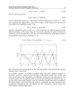
The photons survived in resonance. This is why a lens can focus an optical beam: the
relative phase delays are compensated by direction change of the wavevector so that the
curvature of the wavefront changes as shown in Fig.1. There exists angular momentum due
to strong electromagnetic interaction.