Photodiodes World Activities in 2011 Part 3 pdf
Bạn đang xem bản rút gọn của tài liệu. Xem và tải ngay bản đầy đủ của tài liệu tại đây (2.32 MB, 30 trang )
Photon Emitting, Absorption and Reconstruction of Photons
51
interaction of light field with electron or atomic systems that demonstrated anti-bunching
light, the most promising is the electrically driven single-photon source (Zhiliang Yuan et
al., 2002). In their experiment, the HBT measurement demonstrated indeed sub-Poissonian
photon statistics and anti-bunching. Most of the experiments reported to date demonstrate
antibunching using radiation field interaction with atomic or ion system which limit the
number of the photon emitting. Is there any reason that from the property of the photons by
themselves that should result in antibunching? Why the photons can distinguish each other?
Destructive two-photon interference demonstrated photon antibunching with calculated
2
01g . Actually, they obtained both the bunching and antibunching by controlling the
phase difference between two input beams so that the production process is difficult to
understanding by a naïve photon picture (Kaoshi & Matsuoka, 1996).
To answer these questions, one should also consider the physical observables that are
quantized wavevectors or polarization vectors. Electromagnetic fields never refuse to
interfere with each other. There are two cases that should be considered. One is the
coherently combination, the other is the interference coherently. If we consider the
monochromatic wave as single mode, the two linearly polarization orthogonal each other to
form a new state only when their wave vectors lay on line. For the linearly polarized light
with wave vector in different direction in same plan, they can coherently interfere to
produce fringes when across each other, while keeps their independent so that keep their
polarization and wave vector unchanged after crossover. However, if these waves
topologically charged they can combine to share a same angular momentum. The optical
vortices formed under strong electromagnetic interaction where the wavevectors
topologically combined. The optical vortex with angular momentum equal to 1 refuses to
take same position with the optical vortex with angular momentum equal to -1 in the space
so that vortex lattice formed as shown in Fig.5. This phenomenon can be considered as
spatial anti-bunching. However, there should be collective behavior of large amount of
photons since the optical vortices are the results of strong electromagnetic interaction
provided by photons themselves. Here, the optical vortices with different angular
momentum can distinct each other. The optical vortices are now mostly considered due to
orbital angular momentum.
6. Directional emission of photons
The divergence of photon emitting from a cavity can be easily estimated from uncertainty
principle of the quantum mechanics.
2
x
xp
(34)
Supposing the size of the antenna is
Rx
, the divergence angle /
xx
p
p
and
2/
x
pk, it is immediately to have
4 R
(35)
Therefore, the divergence angle increases with decreasing the size of the antenna. The
divergence angle of photon emitting from quantum dots is very large that a photon shared
by all possible modes. As a result, the collection efficiency of the photon is very low.
Photodiodes - World Activities in 2011
52
Put a quantum dot in cavity or waveguide that may limit the photon to emit only to desired
modes. But that is difficult in technical realization. Using surface plasmon resonances to
form optical patch antennas is promise (Esteban et al., 2010). The unidirectional emission of
a quantum dot coupled to a nanoantenna was experimentally demonstrated (Curto et al.,
2010). In their experiment, a quantum dot was placed in the near field of one of the five-
element gold Yagi-Uda antennas for operation wavelengths of ~800 nm. The total length of
the antennas is 830 nm. The antennas emission a beam with an divergence angle at half
maximum of 12.5º×37º pointing into the glass substrate. The simulations indicated that as
much as 83.2% of the QD emitted light were collected.
This coupling demonstrates a mode selection. The surface plasmon can only be excited by
TM waves. As a result, quantum dot emission is transformed onto TM mode via surface
plasmon resonance. The interaction of the five-element emission decided the direction of the
optical beam. The mode selection is from two physical reasons:
1.
Photons are survived in resonance. Once the TM mode resonant with surface plasmon,
it absorbs all energy of the photon possess, TE mode is depressed.
2.
The interaction of the radiation field emitted by the antennas decided the emission
direction and divergence. That is decided the mode structure of the photon.
Divergence from an emitter can not be avoidable. The detector requires convergence of the
beam. There is still a need to study the wavefronts and the mode structure, if one considers
the reciprocity: that is if a next similar five-element Yagi-Uda can sense the emitted beam so
that results an absorption in a quantum dot under the assumption adiabatic unitary
transformation?
There has no evidence that an adiabatic unitary transformation is technical realistic. Loss
and dephase are unavoidable. However, many experiments have demonstrated with single
photon detector now available commercially, many quantum information experiments can
be successfully performed.
7. Single photon detector
Single photon detectors are essential for quantum information applications. Single photon
detectors at the communication wavelengths have attracted much attention in recent years.
Here we introduce some of the results on developing single photon detector at
communication wavelengths in our laboratory.
7.1 Characterizing an APD for single photon detection
Single photondetectors used in quantum key distribution ask for very high sensitivity and
extreme low noise. The InGaAs avalanche photodiodes (APD) are usually chosen for single
photon detection at the infrared communication wavelengths. This APD has a structure of
separate absorption, grading, and multiplication (SAGM). The SAGM APD has been studied
extensively and successfully used for single photon detection in the infrared communication
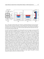
wavelengths. The structure of this APD is depicted in Fig.6. The absorption layer InGaAs is
designed to have a bandgap of 0.73 eV so that the sensitivity can extend to about 1650 nm. A
grading layer between the absorption layer and the multiplication layer facilitates the holes
induced by absorption of photons to transit into the multiplication layer (Hiskett et al.,
2000).
Photon Emitting, Absorption and Reconstruction of Photons
53
Fig. 6. (a) The structure of the SAGM APD, (b) the band diagram of the APD, (c) The inner
build electric field under zero bias and under punch-through.
This APD has to be operated in Geiger mode to exploit the extreme sensitivity. A Geiger
mode means the APD is operated at a bias higher than its breakdown voltage that any
carrier in the multiplication layer will initial self-sustained avalanche. As a result, the APD
should have extreme low dark current. Therefore, there are only a few choices of APDs
commercially available for operation in Geiger mode. The APDs have to be operated at low
temperature. The APD will be damaged if there is not quenching voltage immediately after
the avalanche to stop the self-sustained current. Therefore, the Geiger mode is usually
realized in gated mode operation. The gated pulses applied on the APD are synchronized
with the arriving of the signal photons.
However, the breakdown voltage itself is not very clearly defined. Theoretically, breakdown
voltage is said at that voltage the multiplication factor goes to extreme large, or self-
sustaining avalanche appeared. But in experiment, it usually included various guess work.
For example, the breakdown voltage is defined as the bias voltage at which dark current is
100 μA (Maruyama et al., 2002). Or, the voltage when the first pulse with peak value of 100
mV (0.5 mV at the APD) was detected (Rarity et al., 2000). The voltage higher than the
breakdown voltage is called excess voltage or the relative excess bias. Exploring the use of
the excess voltage for higher sensitivity has also been reported. Therefore, the
characterization of the APD at voltage higher than the breakdown is also needed. However,
the characterization of the I-V curves is usually stopped at the guessed breakdown voltage
to prevent APD from being damaged. Here we introduce the I-V characterization including
the excess voltage with breakdown voltage well defined by actual measured value.
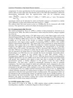
A passive quench circuit with a 200 KΩ quench resistor is used to characterize an APD of
type C307645E from EG&G. The APD was cooled to a temperature of -25
℃ by Peltier effect.
A 1.31 μm pigtailed DFB diode laser attenuated to -45dBm was used as input signals which
switches on to measure photon-current-voltage curves, and switches off to measure dark-
current-voltage curves. The measured results are shown in Fig.7 which is very similar to
other corresponding reports.
The punch through voltage and the breakdown voltage are not clearly indicated in the I-V
curve shown in Fig.7. We define a parameter called relative current gain
Photodiodes - World Activities in 2011
54
1
r
dI
G
dV
(36)
Fig. 7. The breakdown voltage and the bias were decided from these I-V relations
experimentally.
The reason is obvious. The multiplication factor has reached it maximum after breakdown,
the gain is saturated. The detector performs as a linear device before avalanche and after
breakdown. The relative current gains are plotted with the applied voltage both for the
photon-current and the dark current as shown in Fig.8 where the data are the same as in
Fig.7. The breakdown voltage and the punch through voltage are much more clearly
indicated.
The breakdown voltage makes no difference between the photon induced carriers and the
dark carriers. But the dark carriers start to avalanche at higher bias. This features a depletion
region exists at the vicinity of the heterojunction of the InGaAs/InGaAsP.
7.2 Operation parameters of APD for better performance
It is usual in designing a single photon detector, the operating voltage and the
temperature should be carefully considered. The operating voltage should higher than the
breakdown, that is an excess voltage is needed. With increasing the excess voltage, the
sensitivity seems to be increased, but the error bits or dark counts increased also. There is
still uncertain that how high the excess voltage is the best. Thermal excitation decreased
with cooling the temperature. It seems the lower temperature is the better. But from the
consideration of practical application and the phenomenon the dark carriers not start to
avalanche immediately after punch-through, it is reasonable to optimize the operation
temperature.
Photon Emitting, Absorption and Reconstruction of Photons
55
Fig. 8. The relative current gain versus bias characterization curves clearly indicating the
punch through voltage, breakdown voltage and the avalanche.
In according to the I-V property shown in the Fig.8, one should consider both the bias and
the operation temperature at the same time. Because the breakdown voltage decreases with
temperature, the breakdown voltage can be adjusted by cooling the APD so that it is larger
than the punch through voltage but not too high to avoid the breakdown initiated by dark
carriers. In the Fig.8, the breakdown voltage of about 50 V is a reasonable choice. The excess
voltage needed is very limited.
It is well known that the photon absorption follows an exponential law while the thermo-
generated carriers follow Gaussian distribution. A calculation analysis is shown in Fig.9
where we calculated the distribution for incident of average 0.1, 0.3, 0.5 photons per pulse
and suppose the thermo-generated carriers in the pulse duration are 1, 0.75, and 0.5,
corresponding to the curves (a), (b), and (c) respectively. The S/N ratio is defined as the
photon-induced carriers divided by thermal carriers that can drift into the multiplication
layer. It is clear that the S/N is fairly high if the bias voltage do not penetrate into the
absorption layer too much.
The excess voltage can be controlled by temperature since the breakdown voltage is a
function of the temperature. That is the basis the temperature control could be used to
adjust the breakdown voltage. The bias larger than that of the punch-through is necessary
and the depth of punch through should be carefully chosen.
Photodiodes - World Activities in 2011
56
Fig. 9. The spatial distribution of the photon-induced carriers and thermal carriers in the
absorption layer calculated on the basis of average number per pulse duration indicating
that the depth of the punch-through voltage penetrate into the absorption is very limited for
a reasonable S/N.
7.3 Integral detection
The gated electric pulses may produce electric spikes that would result in error counts.
Therefore, single photon detector with balanced two APDs has been reported that S/N ratio
improved by more than one order of magnitude in compared to the conventional usage of
APDs (Tomita & Nakamura, 2002; Kosaka et al., 2003). Although various proposals had
added to the balancing structures, they are not only technically complex, the spikes can not
be cancelled completely. The integral gated mode single photon detection is much
promising for use in quantum key distribution (Wei et al., 2007).
In the method of the integral gated mode detection, an integral capacitor stores the charges
of the avalanche current and gives a negative feedback to the APD bias that leads to quench
the avalanche at a fixed level. The integral capacitor and a charge amplifier compose as
integrator so that the detected signals are static charge on the capacitor. There are no spikes
at all and easy for digital processing afterwards.
In the experiments with the integral gated mode single photon detector, the single photon
source was attenuated faint pulses with width of 50 ps at 1550 nm from a gain-switched
laser (Sepia PDL808, Picoquant). The APD used in the experiments was from JDS Uniphase
(ETX 40 APD BA, ETX00408052-005). The temperature of the APD was stabilized at 224±0.1
K. The static bias was 43.1 V which is below the punch through voltage. The gated pulses of
5.13 ns in FWHM and 4.4 V peak-to-peak were added to DC bias. The breakdown voltage of
Photon Emitting, Absorption and Reconstruction of Photons
57
this APD measured at 224 K is 46.6 V. Therefore, there is only an excess voltage of 0.9 V. A
gate pulse frequency of 100 kHz was chosen in the measurement.
The traces of the APD avalanche recorded by oscilloscope TDS1012 show clearly the
transient spike cancellations. A single photon detection efficiency of 29.9% at dark count
probability of 5.57×10
-6
per gate or 10.11×10
-7
has been achieved.
8. Multipartite entanglement of photons
The single photon detector records classical information. It records only the energy. In
quantum information, there should have records of quantum bits. Therefore, two or more
detectors have to be used, and these detectors should be entangled each other. This can be
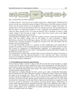
realized with some kind of interferometers. For example, the Mach-Zehnder interferometer
as shown in Fig.10, the record at the detector A should be entangled with that at detector B.
If detector A records 1, then detector B should record 0. That is, only record of (10) is correct,
while all other records including (01), (00), (11) are error bits.
Fig. 10. Mach-Zehnder implementation of quantum key distribution
To obtain a correct record, Bob has to decode by using phase modulation in according to
their protocol so that the maximum of the interference is at detector A corresponding to the
input quantum signals:
1
11
1
0
2
1
i
i
i
e
e
e
(37)
One photon can be coherently shared among N spatially distinct optical modes to form
multipartite entanglement, a quantum state being called W state. A W-state with N=4 can be
expressed in the form
12
1
1000 0100 0010 0001
2
ii
i
Weee
(38)
The multipartite entanglement with N=4 where the partite is formed by beamsplitter has
been detected and characterized in more detail (Papp et al., 2009).
A genuine N-partite entanglement is realized only with simultaneous participation of all N
of the constituent systems. There is also a similar case where is N time-distinct partite
entanglement. There are N time-distinct faint pulses to share one photon. This kind of
multipartite entanglements is realized in differential phase shift key distribution system
where the simultaneous participation of the constituent systems is due to the nonlocality of
the photons.
Φ
A
B
Photodiodes - World Activities in 2011
58
However, the utilization ratio of the traditional differential phase shift is low. Their key
creation rate under ideal condition can only reach (1-1/N) if a single photon pulse is split
into N sequential ones. The utilization ratio of photons can reach 1 under ideal condition by
discrimination and controlled delay of the first pulse (Wang et al., 2009). This scheme can
also result in a genuine N-partite entanglement with N time-distinct constituents. In the
proposed scheme of 6-partite entanglement, the two pulse trains containing three time-
distinct pulses in each formed by beam splitter and controlled time delay. The multiplex at
Bob side are designed such that with the first single pulse of the first train two-bit delayed
the rearranged pulse train can recombine with the next pulse train in three time slots
exactly. Their coherent superposition represents an entangled state of a photon in three-
dimensional Hilbert space with four non-orthogonal states:
1
100 010 001
3
A
BC ABC ABC
VHH
(39)
Where,
V is vertical polarization state, H is the horizontal polarization state. All the
constituents of a photon have involved in the key creation so that is a genuine multipartite
entanglement state. Not only the key create ratio is increased, the security is also enhanced.
9. Dephase and decoherence
Dephase and decoherence are unavoidable even in the case under idealized condition
without loss if one consider a rigorous representation of the wavefunction for single
photons. In according to quantum mechanics, a state of a particle is represented as a
complete set of eigen functions. Therefore, the number state of N=1 should be expressed in a
two dimensional Hilber space that
101
(40)
Even in pure vacuum, the fluctuated electromagnetic fields exist that make up the zero-
point energy. Quantum theory predicts that empty space is not truly empty. In an
electromagnetic field, virtual photons created and annihilated constantly that make
contribution to a small renormalization of the energy of a quantum system, known as the
Lamb shift. The experimental observation of the Lamb shift in a solid system has been
reported (Frabner et al., 2008). A scheme including vacuum state that can be used to
demonstrate the nonlocality of a single photon experimentally has also been proposed
(Dunningham & Vedral, 2007).
In their scheme, classical faint pulse incident on beamsplitter has been expressed as two
input ports and two output ports where a state of Eq.(40) and a vacuum state
0 are
incident on the two input ports of a 50:50 beamsplitter, and two output state of U1 and U2
as shown in Fig.11. It is obvious that vacuum fluctuation in the output state is increased. In
their model, they have chosen the particular values that
1/ 3 , and 2/3
i
e
to
simplify the analysis without losing the generality of their arguments. The state after the
beamsplitter is
1
00 01 10
3
i
ei
(41)
Photon Emitting, Absorption and Reconstruction of Photons
59
Where the first ket in each term represents the number of the particles on path U1 and the
second ket represents the number of particles on path U2. It is general the case that any
operation on the state of the photon leads to lose and combining vacuum fluctuation. That is
the quantum permutation.
The phase is important while modes are distinguished only with their polarization and
momentum. In quantum mechanics, states with only a pure phase difference are taken as
the same state also. Now that the constituents of the photon and the vacuum fluctuations
with phase unknown come together in the same mode to superposition that are the reason
the dephase come from.
Fig. 11. Single photon is operated by a beam splitter, the vacuum states are involved.
10. Reconstruction of photons
Vacuum supports all optical modes and each of the modes can contain constituent of any
photon with phase and amplitude arbitrarily defined which are relay on the initial
condition. Therefore a photon emitted from a quantum dot or from a single atom will be
coupled to all possible modes with equal probability. The interaction of all the emitting
mode fields decides the Emitting pattern that has large divergence. The divergent light will
soon be scattered to become a part of the fluctuation in the vacuum if it is not immediately
collected and focused to a detector and absorbed. Any procedure or operation on the
emitted light means mode change and mode structure reorganization.
The actual probability of detecting a photon is decided by the collecting and focusing as
much as possible the constituents of the photon. The highest detection efficiency of a photon
is always at where the superposition of the mode fields has constructive coherence to the
maximum while detection probability of zero may indicate a destructive superposition.
Therefore one should consider the mode structure of a photon and the interaction of the
mode fields. It is usual to limit the mode number so that can make the modes controllable.
It is essential to control the mode selection so that to control the mode structure of a photon.
There are two mechanisms to collect energies of the photon. One is the mode competition.
The other is control the mode volume geometrically such as in waveguides or in cavities
where only limited modes can be excited.
10 β
α
0
U1
U2
Photodiodes - World Activities in 2011
60
In case the quantum dot coupled to the surface plasmon in an element of the Yagi-Uda
antenna, the emitting energy concentrated in resonant TM mode due to excitation of the
surface plasmon so that the TE mode is depressed. This is the resonant enhancement effect.
The direction of emitted light by the Yagi-Uda is decided by interaction of all elements
composing the antenna. Here only one direction has coherent maximum of superposition.
Reconstructions of photons for quantum information are quite usual. The photons are
divided into two or more part and encoded with phase information. On recombining these
constituents of the photon, the coherent superposition decides where the maximum
detection probability should appear to a detector as predicted. The coherent maximum and
the coherent minimum appeared at the same time and in different places showing an
entanglement. A successful unitary transformation will guarantee a photon appeared to a
detector with probability of 1 while the probability is zero at all other places. However, this
transformation can not prevent a detector to sense the vacuum fluctuation.
The vacuum fluctuation has important role in the detection. Since the vacuum contain all
possible modes that deserve the ergodic assumption. That is why the quantum permutation
with vacuum exists always. In fact, the photon reconstruction is decided eventually under
the choice of the detector where the herald mode fields combining necessary energy from
the vacuum fields can form a photon the mode structure of which matches the needs for
resonant absorption. There has not a photon detector that is quantum state sensitive, for
example, a polarization dependent detector. One may consider a detector which is state
sensitive so that can decrease the quantum error bits.
In conclusion, photons are different from other particle with static mass. Photons compose
by themselves of electromagnetic field modes which are quantized by the electromagnetic
interaction. Therefore, mode structure of a photon should be considered so that nonlocality
and entanglement of photons could be explained.
11. References
Chao, C. Y., & Kung T.T. (Gong Zutong), (1933). Interaction of hard γ-ray with atomic
nuclei. Nature, 4, (1933) 709
Combes, J. & Torner, L., (2005). States for phase estimation in quantum interferometry.
Journal of Optics B: Quamtum and Semiclassical Optics. 7, (2005) 14-21
Cronstrond, P. & Jansik, B., (2004). Density functional response theory calculation of three-
photon absorption. Journal of Chemical Physics, 121, (2004) 9239-9346
Curto, A. G.; Volpe, G., Taminiau, T.H., et al. (2010). Unidirectional emission of a quantum
dot coupled to a nanoantenna. Science, 329, 5994, (20 August 2010) 930-933
Dunningham, J. & Vedral, V., (2007). Nonlocality of a single particle. Physical Review Letters,
99, (2 November 2007) 180404
Einstein A., (1997). On the quantum theorem of Sommerfeld and Epstein. A translation of
the paper appears in "The collection Papers of Albert Einstein", Vol.6, Engel, trans.,
Princeton U. Press, Princeton, NJ (1997), pp.434, see also: A. Douglas Stone, Physics
Today, (August 2005) 37-43
Eiseman, M.D., L. Childress, A., Andre, et al. (2004). Shaping quantum pulses of light via
coherent atomic memory. Physical. Review Letters, 93, (2004) 233602
Esteban R., Teperik, T.V., & Greffet, J. J., (2010). Optical patch antennas for single photon emission
using surface plasmon resonances. Physical Review Letters, 104, (15 January 2010) 026802
Frabner, B.,Göppl. M., Fink, J M., et al. (2008). Resolving vacuum fluctuations in an electrical
circuit by measuring the Lamb shift. Science, 322, 5906,(28 November 2008) 1357-1360
Photon Emitting, Absorption and Reconstruction of Photons
61
Ghai, D. P., Vyas, S., Senthilkumaran, P., & Sirohi, R.S., (2009). Vortex lattice generation
using interferometric techniques based on lateral shearing. Optics Communications,
282, (2009) 2692-2689
Gisin, N., Ribordy, G., Tittel, W., & Zbinden, H., (2002). Quantum cryptography. Reviews
Modern Physics, 74(1), (January 2002)145-195
Gong Zutong, (1999). Structure theory of photon, PHOTONICS SINICA, 28(1), (1999) 1-10
Greiner W., (2001).Quantum Mechanics, Fouth Ed. Springer-Verlag Berlin Heidelberg, ISBN
7-5062-7263-6/O·530, New York
Hanbury Brown R. & Twiss, R. Q. (1956). Correlation between photons in two coherent
beams of light. Nature (London) 177, (1956) 27-32
Hiskett, Ph. A., Buller, G. S., Loudon, A. Y. et al. (2000). Performance and design of
InGaAs/InP photodiodes for single-photon counting at 1.55 μm. Applied Optics,
39(36), (December 2000) 6818-6829
Hughes,R. J., Morgan, G. I., & Perterson, C. G., (2000). Quantum key distribution over a 48
km optical fibre network. Journal of Modern Optics 47, 2/3,(2000) 533-547
Kardyna B.E. , Hees, S.S., & Shields,A.J., (2007). Photon number resolving detector based on
a quantum dot field effect transistor. Applied Physics Letters, 90, (2007) 181114
Koashi, M. & Matsuoka,M., (1996). Photon antibunching by destructive two-photon
interference. Physical Review A53, (5), (May 1996) 3621-3624
Kosaka, H., Tomita, A., Namhu, Y., et al. (2003). Single-photon interference experiment over
100 km for quantum cryptography system using balanced gated-mode photon
detector. Electron. Lett. 39(16), (2003) 1199-1201
Mandel, L., & Wolf, E., (1995). Optical Coherence and Quantum Optics, Cambridge, ISBN 0 521
41711 2, New York. pp.476
Maruyama, T., Narusawa, F., Kudo, M., et al. (2002). Development of a near-infrared
photon-counting system using an InGaAs avalanche photodiode. Optical
Engineering, 41(2), (2002) 395-402
Mason E.J., Albota, M. A., Konig, F., & Wong, F.N.C., (2002) Efficient generation of tunable
photon pairs at 0.8 and 1.6 μm. Opt. Lett. 27, (2002) 2115-2117
Migdall A.L., Branning, D., Castelletto, S., & Ware, M., (2002). Single photon source with
individualized single photon certifications. Proc. SPIE Vol.4821 (2002) 445-465
Miller A. J. , Sae Woo Nam, and J. M. Martinis, (2003). Demonstration of a low-noise near-infrared
photon counter with multiphoton discrimination, Appl. Phys. Lett. 83(4), (2003) 791-793
Mori S., Motoya, M., Namekata, N., & Inoue, S., (2004). Generation of correlated photon pairs at
1550 nm by periodically poled Lithium Niobate. Trans IEICE , J87-C(2004)675-685
Muller, A., Herzog, T., Huttner, B. et al. (1997). "plug and play" systems for quantum
cryptography. Appl. Phys. Lett. 70(7), (1997) 703-795
Namekata, N., Fujii, G., & Inoue, S., (2007). Differential phase shift quantum key distribution
using single-photon detectors based on a sinusoidally gated InGaAs/InP avalanche
photodiode
. Appl. Phys. Lett. 91, (2007) 011112
Neves,I., Lima, G., Gomez, A. J. G. et al. (2005). Generation of entangled states of Qbits using
twin photons. Phys. Rev. Lett. 94(10), (2005) 100501
Papp, S. B., Choi, K. S., Kimble, H. J. et al. (2009). Characterization of multipartite entanglement
for one photon shared among four optical modes, Science, 324, 5928, (2009) 764-771
Pathak A. & Mandal, S., (2003). Photon-bunching, photon-antibunching and nonclassical
photon statistics of coherent light couped to a cubic nonlinear medium. Modern
Physics Letters B, 17(5&6),(2003) 225-233
Pittman T.B., Jacobs, B.C., & Franson, J.D., (2002). Single photon on pseudodemand from
stored parametric down-conversion, Phys. Rev. A 66 (2002)042303
Photodiodes - World Activities in 2011
62
Rarity, J. G., Ridley, T.E., Ridley, K.D., et al. (2000). Single photon counting for the 1300-1600-
nm range by using of Peltier-cooled and passively quenched OnGaAs avalanche
photodiodes. Applied Optics, 39(36), (2000) 6746-6753
Roychoudhuri Ch. & Roy, R., Guist. Ed. (2003). OPN Trends: The nature of light, What is a
photon. Optics & Photonics News, 3(1)
Saleh, B. E. A. & Teich, M. C.,(Eds.). (1991). Fundamentals of Photonics, John Wiley & Sons,
ISBN 0-471-83965-5, New York, pp.87-88, 249
Santori C., Peton, M., Solomon, G., Dale, Y., et al. (2001). Triggered single photons from a
quantum dot. Phys. Rev. Lett. 86, (2001) 1502-1505
Tanzilli S., Riedmatten, H.D., Zbinden, H., et al. (2001). Highly efficient photon pair source
using periodically poled lithium niobate waveguide. Electron. Lett. 37 (2001) 26-28
Tomita, A. & Nakamura, K. (2002). Balanced gated-mode photon detector for quantum-bit
discrimination at 1550 nm. Opt. Lett. 27(20), (2002) 1827-1829
Torres, J. P. &Torner, L. (2005). Quantum state engineering for spatial control of entangled
photon pairs. Proceeding of SPIE Vol.5736, (2005) 173-184
Walls D.F., & Milburn, G.J., (1994). Quantum Optics, Springer-Verlag, ISBN 3-540-58831-0,
Berlin Heidelberg, pp.41-58, 199
Walton Z., Sergien, A.V., Atature, M., Saleh, B.E.A., & Teich. M.C. (2001). Performance of
photon-pair quantum key distribution system. J. Mod. Opt. ; 48 (2001) 2055-2063
Wang Jindong., Qin Xiaojuan, Zhang Huani, et al. (2009). A free-space-based differential
phase shift quantum key distribution scheme with higher key creation efficiency.
Optics communications, 282, (2009) 3379-3381
Wei, G. X., Lu, L-L., Guo, Ch-Sh., (2009). Generation of optical vortex array based on the
fractional Talbot effect. Optics Communications, 282, (2009) 2665-2669
Wei Zhengjun, Zhou Peng, Wang Jindong, et al. (2009). An integral gated mode single
photon detector at telecom wavelengths. Journal of Physics, D: Applied Physics,
40(22), (2007) 6922-6925
Wootters W.K. & Zurek, W.H., (1982). A single quantum cannot be cloned, Nature, 299,
(1982) 802-803
Yang, Sh., Powers, P. E., & Zhan, Q., (2009). Experimental verification of focus tailoring
using circularly polarized vortex beams with annular pupil mask. Optics
Communications, 282, (2009) 4657-4659
Yariv, A., (1988). Quantum Electronics, third edition, John Wiley & Sons, ISBN 0-471-60997-
8, New York, pp.96-99
Yi, S. W., Lee, S.K., Yang, G.Y. et al. (2004). Three dimensional micro-fabrication using two-
photon absorption by femtosecond laser. Procedings of SPIE, Vol.5342, (2004) 137-145,
Yoshizawa, A., Kaji, R., & Tsuchida, H., (2003). Generation of polarization-entangled photon
pairs at 1550 nm using two PPLN waveguides. Electron. Lett. 39, (2003) 621-622
Yuan, Zhiliang, Beata E. Kardynal, R. M. Stevenson, et al. (2002). Electrically driven single-
photon source. Science, 295,(4
January 2002) 102-105
Yuan, Zh., Wu. Ch., Zhao, H., Zhao, & Jiang, H., (2005). Imaging of small nanoparticle-
containing objects by finite-element-based photoacoustic tomography. Opt. Lett. 30,
(2005) 3054-3056
Zbinden H., Pasel, S., Gisin, N. et al. (2002). Practical quantum key distribution. Quantum
Optics In Computing and Communications, Proceedings of SPIE, Vol.4917, (2002) 40-44
Zumuth, S., Ansari, Z., Lepine, E. & Vrakking, M. J. J. (2005). Single-shot measurement of
revival structures in femtosecond laser-induced alignment of molecules. Opt. Lett.
30, ( 2005) 2326-2328
Part 2
CMOS Related Topics
4
CMOS Photodetectors
Albert H. Titus
1
, Maurice C-K. Cheung
2
and Vamsy P. Chodavarapu
2
1
Department of Electrical Engineering, University at
Buffalo, The State University of New York
2
Electrical and Computer Engineering, McGill
University, Montreal
1
USA
2
Canada
1. Introduction
The inclusion of cameras in everything from cell phones to pens to children’s’ toys is
possible because of the low cost and low power consumption of the imaging arrays that
form the core of the cameras. However, these arrays are low cost and low power because
they are CMOS-based; this allows for the devices to be made with the same processes and
facilities that are used to make memory and computer chips. Yet, the continued surge in
CMOS imager popularity goes beyond the lower cost to other factors such as ability to
integrate the sensors with electronics, and the ability to achieve fast, customizable frame
rates [1].
In this chapter, we will cover the design and layout of the various types of CMOS
photodetectors and fundamentals of photo-conversion processes in these devices, including
a brief review of CMOS photodetector history. We will then describe the emerging CMOS
based technologies in photodetector design optimization to tune device responsivity,
integration of micro-optics to achieve enhanced detection in low-light conditions,
integration of photonic grating structures on photodetectors for spectral response selectivity,
and bio-inspired CMOS imaging devices. We will conclude the chapter with some examples
of applications of these technologies.
2. CMOS photodetector history
Since the mid-1960s, combinations of p-n (or n-p-n) junctions have been used to convert
light into electronic signals [2, 3]. Work not only focused on the conversion of photons to
electrons, but also on the ability to read the signals out from arrays of pixels. For example,
Shuster and Strull reported in 1965 that they had developed a 2500 pixel array of
phototransistors with 100 leads for readout [4, 5]. For these earliest devices, high gain had
to be used at the pixels because no integration of light (or charge) was used. A year later,
Weckler demonstrated how to operate a p-n junction photodiode in “photo flux
integrating mode” which enabled pixels to be much simpler and ultimately smaller [6].
Photodiodes - World Activities in 2011
66
Photon integration required that the photodiode be turned on for a fixed amount of time
to raise (or lower) the voltage level on a charge storage device; thus, the amount of charge
remaining (or charge that was removed) is proportional to the light intensity over that
integration time.
In the 1970s, CMOS detectors and imaging arrays began to lose popularity to Charge-
Coupled Device (CCD) -based imagers because CCDs could achieve a higher fill-factor; the
fill-factor was lower for CMOS imagers because of the need for transistors at the pixels for
read out and gain. The ability to produce CCD imagers with the necessary number of pixels
for applications (such as TV) gave CCDs a large advantage over CMOS imagers [7]. Noise in
CCDs was also considerable less than in CMOS devices; it was generally regarded that fixed
pattern noise in CMOS imaging devices was worse than in CCDs, which remained true into
the late 1980s and early 1990s. However, improvements in CMOS fabrication technology
and increasing pressure to reduce power consumption for battery operated devices began
the re-emergence of CMOS as a viable imaging device.
It is generally regarded that the first all-CMOS sensor array to produce acceptable images is
the active pixel sensor (APS) imager [8-10]. The APS design used the linear integration
method [6] for measuring light because of the large output signal generated, as opposed to
the logarithmic method [11-16]. The active column sensor (ACS) [17] is similar to the APS
but has lower fixed pattern noise (FPN). As of 2011, we have CMOS image sensors that have
14.6 Megapixels, and higher.
While CMOS and CCDs continue to compete for a share of the image array sensor market,
the ability to design custom integrated circuits (ICs) with photodetectors to perform specific
functions is an enormous advantage over CCD arrays. These ICs are often used in
applications that have specific requirements such as extremely low power consumption [18]
or variable read-out (frame) rates [19] or very fast read-out rates [20]. Normal video rates of
30 or 60 frames per second are fine for standard definition videos, but for some applications,
frame rates of more than a thousand frames per second are needed to capture extremely fast
occurring events (for example see [20]).
CMOS photodetectors are the technology of choice in smart focal plane arrays. In the mid-
1980s, Carver Mead and Misha Mahowald introduced the Silicon Retina that used a
“vertical bipolar transistor” as the light detecting element [21]. This spawned a significant
amount of research into bio-inspired vision chips that used CMOS photodetectors combined
with CMOS signal processing circuitry [22-32]. Generally, these chips are arrays of smart
pixels with significantly more transistors per pixel than the three or four found in typical
APS-based arrays. However, the relative low cost of fabrication for prototyping CMOS ICs
enables chips with one, two, dozens or thousands of detectors to be designed, fabricated and
tested. For chips with few photodetectors, the remaining silicon die area can be used for
signal processing, read-out, or digital interface logic, so there is no wasted space.
Applications of these custom detector and imaging chips range from sub-retinal implant
imagers [33] to glare detection [34] to fluorescence imaging [35, 36] and x-ray imaging [37],
to name a few. A study of three common photodiode structures available in non-
imager/standard CMOS processes provides valuable benchmark data for designers looking
to use CMOS photodetectors [38]. While not an exhaustive study of all possible CMOS
photodetectors, this chapter provides a useful starting point for selecting the best structure
for the application.
CMOS Photodetectors
67
3. Operation of CMOS photodetectors
The core of the sensing element of a CMOS detector is the photosensitive element of the
circuit. Photogates, phototransistors, and photodiodes all can be used as the sensing
element. In this section, the use of a photodiode is discussed. As its name implies, the
photodiode is simply a junction between a p-type and an n-type semiconductor,
commonly known as a p-n junction. Although a simple p-n junction can be used for light
detection, the more sophisticated p-i-n junction with an intrinsic region between the p-
type and n-type region is often used to improve the device efficiency. In this section, the
basic working principle of a photodiode will be discussed, followed by a discussion on
the p-i-n photodiode, and a method of signal amplification resulting in the avalanche
photodiode.
3.1 Photogeneration and recombination in semiconductors
When a semiconductor is illuminated, a photon that has higher energy, h
ν
, than the
bandgap energy, E
g
, may cause an excitation of an electron from the lower energy valence
band to the higher energy conduction band. This results in a pair of the mobile charge
carriers - electrons and holes. This process known as photogeneration can occur if the total
energy and total momentum among the photogenerated electron-hole pair and the incoming
photon is conserved.
The probability of photogeneration by a single photon is a property of the material.
Macroscopically, this is described by the absorption coefficient,
α
. As a light beam
propagates through a piece of homogeneous semiconductor, its power decreases
exponentially as the semiconductor absorbs some of the power for photogeneration. The
power that remains in the light beam after propagating through a depth of z is given by:
=
exp
[
−
(1)
where, P
0
is the intensity at zero depth. Note that the rate of absorption, −dP/dz, decreases
exponentially with depth. Therefore, more photogeneration is expected to occur near the
surface.
Because the photogenerated carriers exist in an excited state, the excess electrons and holes
will recombine after a short period of time (~ picoseconds on average) to release the excess
energy. This process is known as recombination, and it returns the carriers distributions to
thermal equilibrium condition. These excess carriers are lost if they are not captured to
create an electrical signal for light detection. Therefore, a semiconductor device structure is
needed to facilitate the capturing of the photogenerated carriers. The simplest and most
commonly used structure for this purpose is a diode structure known as photodiode (PD).
3.2 Quantum efficiency and responsivity
Before the discussion on photodiode, two important parameters that are used to
characterize the effectiveness of detection by a photodetector should be discussed; these are
quantum efficiency and responsivity. Quantum efficiency is defined as the probability that
an incident photon will generate an electron-hole pair that will contribute to the detection
signal, so it can be expressed as,
=(1−ℛ)
[
1−exp(−)
(2)
Photodiodes - World Activities in 2011
68
where, ℛ is the surface reflectance, is the probability that the generated electron-hole pair
will become a contribution to the detection signal, and d is the depth of the photo-absorption
region. Therefore, quantum efficiency is affected by material properties and device geometry.
The captured carriers are used to generate a signal either as a voltage or a current. The
measure of signal strength to incident power of the device is called responsivity. If the
output is a current, then it is related to the quantum efficiency by the following expression,
=
=
=
.[nm⋅W/A]
(3)
where, q is the electron charge and
λ
is the wavelength in nanometers.
4. Photodiode
Many photodetectors utilizes the formation of p-n junctions, and the simplest of these is a
photodiode, because a photodiode is simply a p-n junction that is designed for capturing the
photogenerated carriers. In CMOS sensing, a photodiode is usually made by forming an n-
type region on a p-type semiconductor substrate, or vice-versa. This can be done by epitaxial
growth, diffusion or ion implantation.
4.1 A quick review of P-N junction
Figure 1 shows the carrier distributions, charge distribution, built-in electric field and band-
diagram of a typical p-n junction. The inhomogeneous charge and carrier distributions are
the result of a state of equilibrium between diffusion, drift and recombination. The
following is a review of the key features of a p-n junction,
1. An absent of the carriers in a region known as the depletion region or space charge
region. It has layer width, W, and ionic space charge of the donors and acceptors are
exposed in this region.
Fig. 1. (a) Diffusion of carriers at the p-n junction, (b) the resulting electron and hole density
distribution, where N
a
and N
d
are the acceptors and donors densities, (c) the resulting
charge density distribution, (d) the resulting electric field, and (e) the band diagram of a p-n
junction showing the alignment of the Fermi level, E
f
, and shifting of the bands. E
v
is the top
of the valence band and E
c
and the bottom of the conduction band.
CMOS Photodetectors
69
2. Due the charge distribution, a built-in electric field, E, has emerged.
3. Alignment of E
f
between the p-type region and the n-type, as the conduction and
valance bands shift in the depletion region.
4. There is a potential difference of V
0
between the p-side and the n-side.
4.2 Operating rinciple
The operation of a photodiode relies upon the separation of the photogenerated carriers by
the built-in field inside the depletion region of the p-n junction to create the electrical signal
of detection. Under the influence of the built-in electric field, the photogenerated electrons
will drift towards the n-side, and photogenerated holes will drift towards the p-side. The
photogenerated carriers that reach the quasi-neutral region outside of the depletion layer
will generate an electric current flowing from the n-side to the p-side; this current is called a
photocurrent. The generation of the photocurrent results in the shift of the I-V characteristic
of the photodiode as shown in Figure 2. Therefore, the I-V characteristic of a photodiode is
expressed as,
=
s
exp
−1−
ph
(4)
where, the first term is the Schottky Equation that described the ideal I-V characteristics
with I
S
being the saturation current, k the Boltzmann constant and T the operating
temperature, and the second term, I
ph
, is the photocurrent.
Fig. 2. Photogeneration in a p-n junction: (a) the built-in electric field driving the
photogenerated carriers from the depletion region away from the junction, and (b) shifting
of the I-V characteristic due to the photogenerated current, I
ph
.
4.3 Basic modes of operation
A photodiode can be operated in three basic modes: open circuit mode, short circuit mode,
and reverse bias (or photoconductive) mode. The circuit diagrams of the three different
basic operating modes are shown in Figure 3.
Open circuit (OC) mode is also known as photovoltaic mode. As the name implies, in this
mode, the terminals of the photodiode is connected an open circuit. In this mode, there is no
net current flowing across the photodiode, but due to the photogenerated current, a net
E
c
E
v
h
Electric Field
N
P
(a) (b)
+
−
Photodiodes - World Activities in 2011
70
voltage is created across the photodiode, called the open circuit voltage, V
OC
. In reference to
Figure 2(a), the photodiode is operating at the point where the I-V characteristic curve
intersects the x-axis.
Fig. 3. Basic operating mode of a PD: (a) open circuit mode, (b) short circuit mode, and (c)
reverse-bias mode.
In contrast, in the short circuit (SC) mode, the terminal of the photodiode is short-circuited.
This allows the photogenerated current to flow in a loop as illustrated in Figure 3(b). In
Figure 2(b), this is represented by the point at which the I-V characteristic curve intersects
the y-axis. The current that flows in the loop in SC mode is also known as the short circuit,
I
sc
, and it has the same magnitude as I
ph
.
In reverse bias mode, a reverse bias is applied across the photodiode as shown in Figure
3(c). Therefore it is operated in the lower left quadrant of Figure 2(b). Note that by applying
a bias voltage, the potential difference across the p-n junction changes to V
0
– V, and the
balance between drift and diffusion in the p-n junction also changes. This will affect the
depletion width (W) and E as well. The dependence of W on the bias voltage can be
described by,
=(
−)
(5)
where, K is a constant, and m
j
depends on the junction geometry (m
j
= 1/2 for a step junction
and m
j
= 1/3 for a linear junction). Therefore, operating in reverse bias has the effect of
increasing W. The increase in W is not as great as the change in the potential difference,
because m
j
< 1, so E should also increase. From the point of view of charge distribution and
Gauss’s Law, a wider depletion region exposes more of the ionic space charge, which in turn
increases the electric field.
The widened depletion region under reverse bias creates a greater photogeneration region,
while the stronger E increases the drift velocity of the photogenerated carriers. In principle,
the drift velocity increases in proportion with E, so even with an increase in W given by
Equation (5), the transit time (the average time that a drifting carrier to reach the end of the
depletion region) is reduced. Therefore signal loss due to recombination in the depletion
region is reduced. Because of these beneficial effects, reverse bias operation is often
preferred.
CMOS Photodetectors
71
4.4 Dark current
4.4.1 Saturation current – diffusion of minority carriers
As shown in Figure 2(b) there exist a small current under revers bias in the I-V characteristic
even in dark condition. This dark current is caused by saturation current, I
S
. On the
boundaries of the depletion region, minority carriers (electrons on the p-side and holes on
the n-type side) can diffuse into the depletion region. Because of the built-in electric field,
these diffused minority carrier may drift across to the depletion region; this is a source of the
saturation current. Therefore, in photodiodes there exist a dark current; however, the
diffusion process is not the only contribution the dark current.
4.4.2 Generation-recombination current
Apart from the diffusion contribution to the dark current, carriers that are generated by
thermal excitation inter-band trap (defect) states in the depletion region can also have a
contribution to the dark current. This trap-assisted process is essentially the reverse of
Shottky-Read-Hall (SRH) recombination. Just like the photogenerated carriers, carriers
created by trap-assisted generation in the depletion region can also be swept away from the
depletion region by drift before they can recombine and form part of the dark current. This
dark current contribution is known as the Generation-Recombination (G-R) current, and it
can be more significant than the diffusion contribution.
4.4.3 Tunneling currents
Under sufficient reverse bias, the E
C
on the n-side can fall below E
V
on the p-side. In this
condition, there is a finite possibility that an electron in the valence band of the p-side can
tunnel through the bandgap into the n-side conduction band. This process is call direct
tunneling or band-to-band tunneling. If sufficient numbers of direct tunneling events occur, its
contribution to the dark current will be measurable.
Tunneling can also occur through an inter-band trap (defect) state. Due to thermal
excitation, a carrier can be trapped in one these states. If this state exists in the depletion
region, and sufficient reverse biased is applied, a trapped electron from the valence band
can have energy higher than E
C
, and tunneling into the conduction band can occur. This is
called trap-assisted tunnel.
4.4.4 Surface leakage current
Due to the interruption of the crystal lattice structure, there can be a high density of surface
charge and interface states at the physical surface of a device. The surface charge and
interface states can affect the position of the depletion region, as well as behaving as
generation-recombination centers. Therefore, the surface of a device can introduce another
contribution to the dark current called surface leakage current. Passivation of the surface can
be used to control the surface leaking current. This is usually achieved by adding a layer of
insulator such as oxide to the surface.
4.4.5 Frankel-poole current
When a sufficiently large electric field is applied to an insulator, it will start to conduct. This
is called the Frankel-Poole Effect. This effect is caused by escape of electrons from their
localized state into the conduction band. Therefore, the Frankel-Poole Effect can occur in a
semiconductor as well. When a sufficiently large reverse bias is applied across a p-n
Photodiodes - World Activities in 2011
72
junction, electrons generated by the Frankel-Poole Effect can also have a contribution to the
dark current.
4.4.5 Impact ionization current
Under reverse bias, the motion of carriers in the depletion can be described as a drift where
the carriers are repeatedly accelerated by the electric field and collide with the atoms in the
crystal lattice. Under strong reverse bias, the acceleration between collisions can be large
enough for a carrier to obtain the energy required to dislodge a valance electron to create a
new electron-hole pair. This process is known as impact ionization and it can generate new
carriers that contribute to the reverse bias current. When the applied reverse bias is beyond
the breakdown voltage, V
bd
, impact ionization becomes a dominant factor of the photodiode
behavior, and the photodiode is said to be operating in avalanche mode.
4.4.6 Summary of dark current
Table 1 summarizes the different dark currents and their dependence. When these dark
currents are taken into consideration, the photodiode no longer follows the ideal diode
characteristic. A detailed discussion on dark current can be found in [39].
Process Dependence
Diffusion
∝exp−
G-R
∝
√
exp−
Band-to-band tunneling
∝
exp−
Trap-assisted tunneling
∝exp−
Surface Leakage
∝exp−
Frankel-Poole
∝exp−
Impact Ionization
∝exp−
Table 1. Summary of dark current dependence, where a, a’, b and c are constants.
4.5 Noise
There are two basic noise generating mechanisms in a photodiode: the statistical fluctuation
in the number of carriers and photons, and the random motion of the carriers. The statistical
fluctuation in particle numbers is the cause of shot noise. The root mean square of the
current fluctuation due to shot noise is
,
=
2
∆ (6)
CMOS Photodetectors
73
where, I
avg
is the average signal current and Δf is the bandwidth of the signal. The signal-to-
noise ratio (SNR) of shot noise is given by,
SNR =
∆
. (7)
The random movement of carriers produces thermal noise also known as Johnson-Nyquist
noise. The root mean square of the current fluctuation due to Johnson-Nyquist noise is
,
=
∆
(8)
where, R
L
is the load resistance.
4.6 Capacitance and dynamic esponse
In high-speed light detection application of the photodiode, the dynamic response of the
photodiode is of the utmost importance. The dynamic response of the photodiode depends
on the drift velocities of the photogenerated carriers, the junction capacitance that is
associated with the space charge in the depletion region, and the diffusion of
photogenerated carriers from the quasi-neutral regions into the diffusion region. The delay
related to the drift can be characterized by a transit time, the amount of time that it takes a
photogenerated carrier to reach the quasi-neutral region. It is simply given by,
=
=E (9)
where, v
drift
is the drift velocity, x is the distance from the point of photogeneration to the
quasi-neutral region, and
μ
is the mobility of the carrier. Then, the longest possible transit
time is,
(
max
)
=E. (10)
Another delaying factor is due to the bias voltage dependence of the depletion layer width.
A change in bias voltage will change the depletion region width as described by
W
=
K
(
−
)
Equation (5), which in turn changes the amount of exposed space charge. This
change in the amount of space charge due to a change in the bias voltage can simply be
modeled by the junction capacitance. The junction capacitance is given by,
=
(11)
where,
ε
is the dielectric constant, A is the cross-sectional area of the p-n junction.
Photogenerated carriers in the quasi-neutral region are normally lost by recombination.
However, on occasion, the minority species of the photogenerated electron-hole pair can
diffuse into the depletion region and contribute to the photogenerated current. Although the
contribution to the overall signal by these carrier diffusion is small, a delay due to this
diffusion process is observable [40, 41]. The time that takes a minority carrier in the quasi-
neutral region to diffuse into the depletion region is approximately,
=
(12)
where, x is the carrier’s distance to the depletion region boundary, and D is the diffusion
constant.
Photodiodes - World Activities in 2011
74
5. Accumulation mode for signal integration in imaging
The basic operating modes are very useful for real time measurement of light intensity that
falls on a photodiode. However, in imaging applications, an integrated signal from the
photodiode is often preferred. The integrated signal from the accumulation of
photogenerated charge provides a form of statistical binning. This statistical binning not
only provides a stronger accumulative signal, but the accumulative signal is a more faithful
representation of light intensity that falls on the pixel within the time period of signal
integration than an instantaneous measurement, especially for weak or noisy signals.
Moreover, in imaging applications, the integration period of the pixels can be synchronized
using a shutter. In this case, the stored charge can then be read one by one after the
exposure. The result is an image.
Charge accumulation can be achieved in the accumulation mode, and it is used in CCD and
CMOS imaging.
Fig. 4. An abstract representation of a circuit for accumulation mode operation of a
photodiode
Figure 4(a) shows an abstract representation of a circuit for operating a photodiode in
accumulation mode. This circuit represents the circuit element of a pixel in an imaging
array. The goal of the circuit is to accumulate the photogenerated carriers (as charge) within
a set period of time and readout the amount of charge collection as the voltage V
out
. Here is
a description of an operation cycle, assuming that there is an optical shutter for exposure
control:
1. To begin, the reset switch is closed. The photodiode is in reverse bias, and V
D
= V
DD
.
2. The reset switch opens, follow by the shutter. V
D
starts to drop.
3. After t
int
, the shutter closes, followed by the read switch, and V
out
= V
D
.
4. Read switch opens, and then reset switch closes. Circuit returns to initial state.
To measure the light intensity of the pixel for single image, only one cycle of operation is
needed. To measure a series of images (e.g. in video recording), the operation cycle can be
repeated continuously. During the integration phase, the rate of voltage drop depends on
I
ph
, I
d
and C
PD
, which can be described by the following differential equation,
CMOS Photodetectors
75
=−
(13)
Note that C
PD
varies with the bias voltage. As discussed in [42], this voltage drop is usually
linear for a wide range of values below V
DD
. Therefore, the voltage readout at the end of the
integration period can be used as a measurement of the amount of light that has fallen on
the pixel during the integration phase.
6. CMOS active pixel sensing
There are many ways to implement CMOS pixel sensing using accumulation mode. The
simplest active pixel sensing implementation is the T3-APS, as shown in Figure 5. In this
implementation, a MOSFET is used to control the reset current. Another MOSFET is used as
a source follower (SF) to keep the output voltage the same as V
D
, and the control of the
readout is control by yet another MOSFET (Select). The SF-FET prevents discharge during
the readout; therefore it is possible to re-read the same pixel twice without losing V
D
.
Because of difficulty in suppressing thermal noise and other design limitations [43-45], the
T3-APS has been superseded by other implementation such as T4-APS [43, 44, 46].
Fig. 5. T3-APS implementation of CMOS pixel sensing.
7. P-i-N photodiode
Increasing the active region where the signal generating photogenerated carriers originated
from should in principle increase the collection efficiency. Previously, increasing the active
region by increasing W through reverse biased was discussed. To further increase the active
region, the device geometry can be altered to include an intrinsic region between the p-type
and n-type regions, as shown in Figure 6, this results is a p-i-n junction.
Figure 6(e), shows a band diagram of a p-i-n junction under reverse bias. Under reverse bias,
certain assumptions can be made because the external field has driven almost all the carriers
from the intrinsic region [47]. These assumptions are,
• No net charge in the intrinsic region.
• A very narrow depletion region on the doped side of each of the doped-intrinsic
junctions.
With these assumptions, the depletion layer width is simply the width of the intrinsic
region; the electric field in the intrinsic region is simply,