Superconductivity Theory and Applications Part 13 ppt
Bạn đang xem bản rút gọn của tài liệu. Xem và tải ngay bản đầy đủ của tài liệu tại đây (1.75 MB, 25 trang )
Current Status and Technological Limitations
of Hybrid Superconducting-Normal Single Electron Transistors
289
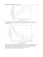
Fig. 5. Plan view of the Stability Diagram for a h-SET. For clarity purposes,
Δ
is given in eV,
so to compare directly with V
SD
.
In the next section we will analyze some of the possible effects that can alter the process of
controlled transport of electric charges in a h-SET turnstile configuration.
The extension of the Coulomb blocked region to V
SD
values ≠ 0 is the peculiar feature of the
hybrid assembly. This opens the possibility for such a device to operate as a turnstile. In fact,
we can operate the device along the pathway between points A and B with V
SD
≠ 0 (Fig. 5).
From points A and A' (B' and B) tunneling inhibition is accomplished thanks to the Coulomb
Energy e
2
/2C (ΔF<0), whereas in the intermediate region A'B', the presence of the
superconducting gap is the limiting mechanism (0<ΔF<Δ).
2.3.3 Error sources in hybrid SET
The following treatment on the error sources in Hybrid SET will not be exhaustive, since
second-order (e.g. co-tunneling), and technology-related (e.g. Adreev’s reflections at the
oxide pinholes) effects, will not be discussed. We will focus on a sort of “ideal” h-SET, in
order to determine the optimal conditions for turnstile operation.
Superconductivity – Theory and Applications
290
It is rather intuitive that small V
SD
values lead to an increased probability for tunneling
events in the backward direction, according to the relationship (Pekola et al., 2008):
()
exp /
bSDBN
eV k TΓ∝ −
(20)
where Γ
b
is the rate of backward tunneling k
B
the Boltzmann constant and T
N
the
temperature at the Normal electrode. On the other hand, the rate of unwanted intra-gap
events increases when V
SD
approaches 2∆, as described by eq. (19). Thus, the probability of
both kinds of spurious events described by eqs. (19) and (20) reaches a maximum value
either for V
SD
= 2∆ or V
SD
=0, respectively. Minimizing the contributions displayed in eqs.
(19) and (20) leads to V
SD
=∆.
It could seem, at a first sight, that the incorporation of superconductors with larger ∆ is, at
first sight advisable, if a drastic suppression of thermal error rates is required as in the case
of metrological applications. This because larger ∆ values would in principle allow
operating the device at higher V
SD
bias.
Examples of h-SETs in literature generally employ Al as the superconductive component
(∆ ≈ 170 μeV). Apart from the ease of producing efficient dielectric junction barriers by
means of simple Al oxidation, the ∆ value for Al is relatively low, if compared e.g with Nb
(∆ ≈ 1.4 meV). As a matter of fact, there are limitations in employing larger gap
superconductors (Pb, Nb) in state-of-art hybrid SETs. Such limitations are either of
fundamental or of technological nature. In the followings we will discuss both these aspects.
2.3.4 A scaling rule
The capability of a h-SET device to act as a single elecron turnstile is related to the
possibility of switching the system between two stable states A and B (Fig. 5), keeping the
system in a blocked region of the stability diagram. All paths at nonzero V
SD
values which
connect A and B, necessarly contain a set of states where the current is suppressed by means
of the superconducting gap, solely. In the present chapter we consider the simplest
theoretical and experimental setup for a turnstile with dc bias and ac gate voltage: in this
framework the system switches between two blocked states, the first related to the Coulomb
blockade in analogy with the n-SET and depicted by means of the AA' and BB' segments, the
second represented by the A'B' segment in which the tunnel current is suppressed by the
superconducting gap. As previously discussed the superconductive gap cannot be
considered as a perfect barrier and the transition in the A'B' segment is a potential source of
current leakage inside the tunnel junctions, then some considerations are needeed in order
to minimize this effect mantaining the advantages of h-SET turnstile configuration.
Minimizing the resident time t
Δ
in this region is then an important issue in order to reduce
errors related to leakage effects. Authors (Pekola et al., 2008), suggested a squared
waveform for the V
g
signal, even if the sinusoidal signal can be more easily handled during
a turnstile experiment.
Evaluation of such resident time is easily obtained in the case of sinusoidal waveform, by
considering the extension of the A’B’ region in Fig. 5. We consider a value for
V
SD
=Δ (with Δ
in eV), say, we assume the SET as working in the optimal conditions according to eqs. (19)
and (20). From geometrical considerations, as can be evident when observing Fig. 5, the
condition:
Δ < E
c
. (21)
Current Status and Technological Limitations
of Hybrid Superconducting-Normal Single Electron Transistors
291
Fig. 6. Comparison between the Current-Voltage characteristics of a Normal (top) and
hybrid (bottom) SET, taken at different gate voltage values. According to the Stability
Diagram of Fig. 2 we observe the broadening of the Coulomb gap with varying V
g
. In the
hybrid assembly the contribution from ∆ broadens the region of inhibited tunneling.
Superconductivity – Theory and Applications
292
must hold, otherwise the system will never reach a stable Coulomb-blocked state. Such
simple relationship provides an important scaling rule for designing h-SETs. It says that
employing high gap superconductors (Nb is a key example) into a hybrid assembly does not
guarantee better device performances. That is, the Charging Energy E
C
must be increased,
too. As an example, if we envisage to replace Al with Nb (2∆ ≈ 340 μeV vs. 2∆ ≈ 3 meV), we
have to find a way to increase the E
C
value by a factor of ~10; this can be accomplished by
decreasing the tunnel capacitance values, solely.
The ratio between t
Δ
, the time interval in which the system is blocked only by the
superconductive gap during a cycle, and the cycle half-period T/2, can be written as:
[]
1
2 / cos( / ) cos( / )
cc
tT ar E ar E
π
Δ
=−Δ−Δ
(22)
and displayed as a function of the junction capacitance and the superconducting gap
Δ(Fig. 7). The 2t
Δ
/T
ratio is <1 (indicative for the presence of a Coulomb Blockade region in
the Stability Diagram, see Fig. 5) only in the portion of the Δ-C plane in which the values of
Δ, and/or C are low. As a comparison, Δ-values for typical low-T
c
superconductors are
indicated together with the reasonnable lower limits for junction capacitance with the most
common SET technologies, the SAIL (Self Aligning In-Line) (Götz et al., 1996) and the
Shadow evaporation (Dolan, 1977).
Fig. 7. The graph displays the calculated dependence of The 2t
Δ
/T
on the superconductor
gap Δ and the junction capacitance C. Lines perpendicular to the Δ-axis show the typical gap
values for most common low-T
c
superconductors, whereas the lines across the C-axis
represent the limit of two typical techniques for producing SETs (see text for details).
Current Status and Technological Limitations
of Hybrid Superconducting-Normal Single Electron Transistors
293
The following chapter will review the technological approaches to realize SET devices, with
the purpose of identifying the most promising ones as far as the capacitance reduction issue
is concerned.
3. SET Technologies
3.1 The Shadow evaporation technique
The shadow evaporation technique (Dolan, 1977) was the first to be used for the fabrication
of single-electron devices based on metallic systems and is currently the most widespread.
This technology takes advantage from a shadow effect, implying that the deposition
techniques must be highly non-conformal. The typical deposition process is then thermal or,
better, e-beam evaporation: this dramatically limits the choice of materials to be deposited
(Nb, for example, being a refractory material, is hardly evaporated).
Fig. 8. SEM image of a suspended mask for Shadow evaporation.
Superconductivity – Theory and Applications
294
The critical step for the success of the process is to fabricate suspended segments of electron
beam resist at a certain distance from the substrate. In common lift-off process, the films are
defined by evaporating the metal through the openings in the mask at normal incidence
substrate, so as to ensure the break between the parts of the layer on the substrate and those
on the mask.
The creation of masks with suspended bridges is possible thanks to the use of two different
types of resists for electron beam lithography, the lower with greater sensitivity to electron
beam than the upper one. During the development step, the exposed resist region is
chemically removed in a selective way, with a wider pattern in the polymer underneath. In
this way, using the so-called proximity effect, typical of electron beam lithography, it is
possible to obtain suspended bridges structures.
Fig. 8 shows the SEM tilted view of the mask we are dealing with: it consists of a support
resist layer of thickness δ
1
~350 nm, on which the layer that define the structures, with
thickness δ
2
~200 nm is lying.
If the mask is suspended one no longer needs to deposit the metal at normal incidence to
guarantee the successful lift-off and can vary the angle of deposition thus obtaining different
patterns on the substrate. From simple geometrical considerations we can see that creating
an opening of width W
0
in the top layer of resist and carrying out the evaporation at an
angle Θ respect to the normal will produce a deposided feature of width:
02
tan( )W
δ
=Θ
(22)
If the angle of incidence is greater than the critical one:
002
arctan( / )W
δ
Θ>Θ =
(23)
the opening in the mask appears as "closed" and the deposition does not reach the substrate.
Fig. 9. Schematics of the angled Shadow evaporation process
Current Status and Technological Limitations
of Hybrid Superconducting-Normal Single Electron Transistors
295
The practical realization of this effect depends on the ability to produce shadow masks
similar to the ideal ones presented so far. To apply this calculation it is important that the
experimental values of δ
1
and δ
2
are reliable, and that the cross section of the top resist layer
is rectangular.
For the construction of tunnel junctions, first a pattern mask with two, very tight openings
must be created. A bridge in the top layer resist between them is then defined.
One can then proceed to the fabrication of tunnel junctions with a deposition-oxidation-
deposition sequence, which occurs in the same vacuum cycle. After the first evaporation
performed to an angle
δ
1
, (Al in Fig. 9) the deposited film is oxidized in O
2
atmosphere then
growing an insulating layer, commonly Al oxide, ~1nm thick. After pumping down, the
second layer is then deposited at angle
δ
2
(Cu in Fig. 9).
3.2 The Self Aligning In Line Process (SAIL)
The principle of the SAIL technique (Koch, 1987) is to fabricate the tunnel junctions at the
two sides of the island, so that the size of the junctions is determined by the thickness and
width of metal thin films: in this way one gets a planar configuration with vertical barriers.
In this section we will discuss the basic steps of the process originally created and provide
some hints on how it could be used for manufacturing h-SETs.
The SAIL process, as presented by Gotz (Gotz et al., 1995) consists of the following steps:
i.
Preparation of a narrow and thin metal film on the substrate (Fig. 10 (a)).
ii.
Fabrication of a resist mask which leaves the area open for the following counter
electrode deposition step (Fig. 10 (b)).
iii.
Anisotropic etching of the film in order to define the island (Fig. 10 (c)).
iv.
Formation of a dielectric barrier on the exposed surface of the island (Fig. 10 (d))
v.
Deposition of the second metal film (Fig. 10 (e)).
vi.
Lift off (Fig. 10 (f)).
There are no particular requirements for the island deposition technique, e.g. sputtering or
evaporation, while the subsequent transfer of the pattern can be accomplished with lift off
or anisotropic etching.
The mask generated in the second step defines the location and size of the island and that of
source and drain electrodes. The process is self-aligned along the length of the island, while
mismatches in the cross direction can be easily compensated by choosing one of the two
metal strips wider: then one can realize an island sandwiched with two wide electrodes
(WNW), as shown in Figure 9, or a large island between two narrow electrodes (NWN),
obtaining in both cases the same junction area.
Difficulties could arise from the use of the same mask for etching and lift off: in fact, the
resist must remain soluble and thick enough to allow reliable lift off, even after the ion beam
bombardment. One will then need to tune the thickness of the resist or the metal depending
on the etching selectivity. The solution may be to replace the ion beam etching, barely
physical, with Reactive Ion Etching (RIE), taking advantage from the chemical selectivity of
the gas employed.
An alternate solution is the use of a multi-layered mask, e.g. two layers of resist with an
intermediate layer with lower etching rate. In this way, the lower resist layer is protected
against the ion bombardment, and can be used as lift off mask.
Superconductivity – Theory and Applications
296
Fig. 10. The main technological steps for the SAIL technique. See text for details.
In order to be used for lift off, the resist mask should show in section walls with negative
slope. The generation of a suitable mask is the crucial step and more complicated in the
SAIL technique than in the shadow evaporation one.
The creation of the barrier after the anisotropic etching of the first mask avoids its damage
due to high-energy ions.
Over-etching in the substrate during step iii. can lead to re-deposition of substrate material
on the exposed sides of the island, and then serious barrier uniformity problems can arise.
To improve the quality of the barrier as well as to minimize the over-etching, it is possible to
choose as substrate the same material of the barrier to be fabricated: in fact, the barrier
dielectrics usually have lower etching rates than the corresponding pure metals, and
therefore can excellently act as etch-stop layers.
A further technological complication is that the formation of reliable contacts requires a
more anisotropic etching (step iii.) than the second metal deposition step (step vi.).
Apart from these difficulties, the SAIL process has several advantages if compared to the
shadow evaporation technique.
Current Status and Technological Limitations
of Hybrid Superconducting-Normal Single Electron Transistors
297
As mentioned above, there is complete freedom in the choice of the deposition process of
metal layer, e.g. evaporation can be replaced by sputtering. It is worth noting, for instance,
that the latter technique is more suitable for depositing a robust and reliable superconductor
like Nb. Moreover, one can get rid of fragile structures like suspended bridges necessary for
the shadow evaporation. Finally, since the tunnel junction is obtained at the sides of the
island, the electrodes overlapping is absent, and the junction capacitance is lower than in
devices realized by the shadow evaporation.
The first SET made with the SAIL technique was reported by M. Gotz (Gotz et al., 1995). The
device is based on the system Al/AlO
x
/Al. The island, with thickness and width of 50 nm
and 80-150 nm, respectively, is defined by EBL and subsequent lift off on a single layer of
AR-P610 resist. The metal was deposited by sputtering. The second mask was made with a
double resist layer composed by AR-P671 and AR-P 641. The thickness of the second metal
layer was 100nm. The anisotropic etching was carried out with Ar
+
ions. Immediately after
the etching, the dielectric barrier has been created by means of oxidation step in dry air. The
reported yield is 40%.
From the width of the Coulomb Blockade areas, the junction capacitance was estimated to
be 0.5 fF, a value in agreement with the calculations for a tunnel junction area of 50 x 150
nm
2
, and a barrier thickness of the order of 1 nm.
4. Conclusions
The employment of the Shadow evaporation technique dramatically limits the choice for
superconductors to use, either from a merely technical (materials to be evaporated) or from
a more fundamental (difficulties in reducing junction areas) points of view. As a matter of
fact, h-SETs made by Al/Cu assemblies have been recently produced and characterized
(Pekola et al., 2008). The SAIL technique seems promising, since it allows for a wider choice
of superconducting materials. It is possible, for example, to envisage the employment of
In:Pb alloys (with improved electrical and thermal properties with respect to the unalloyed
elements) in SAIL SETs by taking advantage from composition-related gap tunability. In this
case, however, technological problems related to deposition of continuous, ~10 nm thick,
films from metals with low fusion temperature require solution. It is noteworthy that such
alloys were used years ago in the first generation Josephson junctions (Lacquaniti et al.,
1982). V or Ta could be interesting alternatives, but the best candidate for the realization of
stable and robust turnstiles should obviously be Nb. Indeed, the graph in Fig. 7 shows that
the inclusion of such material in a h-SET arrangement still requires to overcome the
technological limitations of the SAIL technique.
The possibility of device biasing, offered by the hybrid arrangement can improve the
accuracy of electron pumping process, but care must be taken in reducing leakage through
the superconducting gap. Optimizing between these opposite effects requires the increase of
both the superconducting gap and the charging energy.
5. Acknowlegdments
The work has been carried out at Nanofacility Piemonte supported by Compagnia di San
Paolo.
Superconductivity – Theory and Applications
298
6. References
Altshuler, B. L.; Lee, P. A. & Webb, R. A. (1991). Mesoscopic phenomena in solids. North
Holland, 1991, 978-044-4884-54-1
Averin, D. V.; Korotkov, A. N. & Likharev, K. K. (1991). “Theory of single-electron charging
of quantum wells and dots,”
Physical Review B, vol. 44, n°. 12, pag. 6199, 1991.
Averin, D. V. & Pekola, J. P. (2008). “Nonadiabatic Charge Pumping in a Hybrid Single-
Electron Transistor,”
Physical Review Letters, vol. 101, n°. 6, pag. 066801, 2008.
Blumenthal, M. D.;Kaestner, B.;Li, L.;Gibling, S.;Janssen, T.J.B.M.;Pepper, M.;Anderson,
D.;Jones, G. & Ritchie, D.A. “Gigahertz quantized charge pumping,”
Nat Phys, vol.
3, n°. 5,(2007)
Cholascinski, M. & Chhajlany, R. W. (2007). “Stabilized Parametric Cooper-Pair Pumping in
a Linear Array of Coupled Josephson Junctions,”
Physical Review Letters, vol. 98, n°.
12, pag. 127001, Mar. 2007.
Clark, A. M. (2005).;Miller, N.A.;Williams, A.;Ruggiero, S.T.;Hilton, G.C.;Vale, L.R.;Beall,
J.A.; Irwin, K.D. & Ullom, J.N. , “Cooling of bulk material by electron tunneling
refrigerator “.
Appl. Phys. Lett. 86, 173508 (2005).
Dolan, G. J. “Offset masks for lift-off photoprocessing”.
Appl. Phys. Lett. 31, 337 (1977).
Flowers, J. (2004). “The Route to Atomic and Quantum Standards,”
Science, vol. 306, n°.
5700, pagg. 1324-1330, Nov. 2004.
Geerligs, L. J. ; Anderegg, V. F.; van der Jeugd, C. A.; Romijn, J. & Mooij, J. E. (1989).
“Influence of Dissipation on the Coulomb Blockade in Small Tunnel Junctions“
Europhys. Lett. 10, 79, 1989.
Geerligs, L. J.; Anderegg, V.F.;Holweg, P.A.M.; Mooij, J.E.; Poithier, H.; Esteve, D.; Urbina,
C. & Devoret, M.H. (1990) “Frequency-locked turnstile device for single electrons,”
Physical Review Letters, vol. 64, n°. 22, pag. 2691, Mag. 1990.
Giazotto, F.; Heikkilä, T. T.; Luukanen, A.; Savin, A. M. & Pekola, J. P. 2006). “Opportunities
for mesoscopics in thermometry and refrigeration: Physics and applications“
Rev.
Mod. Phys
. 78, 217 (2006).
Governale, M.; Taddei, F.; Fazio, R. & Hekking, F. W. J. (2005). “Adiabatic Pumping in a
Superconductor-Normal-Superconductor Weak Link,”
Physical Review Letters, vol.
95, n°. 25, pag. 256801, Dic. 2005.
Götz, M.; Bluthner, K.; Krech, W.,Nowack, A.; Fuchs, H.J.; Kley, E.B.; Thieme, P.; Wagner,
Th. Eska, G.; Hecker, K. & Hegger, H. (1996) “Self-aligned in-line tunnel junctions
for single-charge electronics,”
Physica B: Condensed Matter, vol. 218, n°. 1, pagg. 272-
275, Feb. 1996.
Ingold, G. L. & Nazarov, Y. V. (1992) in Single charge tunneling, Vol. 294 of NATO ASI
Series B, edited by H. Grabert & M. H. Devoret, Plenum Press, New York, 1992,
ISBN 0-306-44229-9.
Josephson, B. D. (1962). “Possible new effects in superconductive tunneling,”
Physics Letters,
vol. 1, n°. 7, pagg. 251-253, Lug. 1962.
Keller, M. W.; Martinis, J. M.; Zimmerman, N. M. Steinbach, & A. H. (1996). “Accuracy of
electron counting using a 7-junction electron pump,”
Applied Physics Letters, vol. 69,
n°. 12, pag. 1804, 1996.
Current Status and Technological Limitations
of Hybrid Superconducting-Normal Single Electron Transistors
299
Koch H. "Self-Aligned In-Line Junction - Fabrication and Application to DC-SQUIDS", Int.
Supercond. Electr. Conf., Tokyo August 1987 (Extended Abstracts) pp. 281-284.
Kopnin, N. B.; Mel'nikov, A. S. & Vinokur, V. M. (2006). “Resonance Energy and Charge
Pumping through Quantum SINIS Contacts,”
Physical Review Letters, vol. 96, n°. 14,
pag. 146802, Apr. 2006.
Koppinen, P.; Kühn, T. & Maasilta, I. (2009), “Effects of Charging Energy on SINIS Tunnel
Junction Thermometry “
J. Low Temp. Phys. 154, 179 (2009).
Lacquaniti, V; Battistoni, C.; Paparazzo, E.; Cocito, M.; Palumbo, S. (1982). “Tunnelling
barrier structure of Nb/Pb and Nb/(Pb-In) thin film Josephson junctions studied
by Auger electron spectroscopy and x-ray photoelectron spectroscopy analysis, ”
Thin Sol. Films, vol. 94, n°. 4, pagg. 331-339. 1982
Likharev, K. K. (1988) “Correlated discrete transfer of single electrons in ultrasmall tunnel
junctions,”
IBM Journal of Research and Development, 1988.
Lotkhov, S. V. (2004)“Radio-frequency-induced transport of Cooper pairs in
superconducting single electron transistors in a dissipative environment,”
Journal of
Applied Physics
, vol. 95, n°. 11, pag. 6325, 2004.
Meschke, M.; Guichard, W. & Pekola, J. P. (2006). “Single-mode heat conduction by
photons“
Nature 444, 187 (2006).
Mooij, J. E. & Nazarov, Y. V. (2006). “Superconducting nanowires as quantum phase-slip
junctions,”
Nature Physics, vol. 2, n°. 3, pagg. 169-172, Mar. 2006.
Nahum, M.; Eiles, T. M. & Martinis, J. M. (1994). “Electronic microrefrigerator based on a
normal-insulator-superconductor tunnel junction“
Appl. Phys. Lett. 65, 3123 (1994).
Nahum, M.; & Martinis, J. M. (1993). “Ultrasensitive-hot-electron microbolometer“
Appl.
Phys. Lett. 63, 3075 (1993).
Niskanen, A. O.; Pekola, J. P. & Seppä, H. (2003). “Fast and Accurate Single-Island Charge
Pump: Implementation of a Cooper Pair Pump,”
Physical Review Letters, vol. 91, n°.
17, pag. 177003, Ott. 2003.
Pekola, J. P.; Giazotto, F. & Saira, O P. (2007). “Radio-Frequency Single-Electron
Refrigerator“
Phys. Rev. Lett. 98, 037201 (2007).
Pekola, J. P.; Vartiainen, J. J.; Mottonen, M.; Saira, O P.; Meschke, M. & Averin, D. V. (2008).
“Hybrid single-electron transistor as a source of quantized electric current,”
Nat
Phys
, vol. 4, n°. 2, pagg. 120-124, 2008.
Pothier, H.; Lafarge, P.; Urbina, C.; Esteve, D. & Devoret, M. H. (1992). “Single-Electron
Pump Based on Charging Effects,”
Europhysics Letters (EPL), vol. 17, n°. 3, pagg.
249-254, 1992.
Saira, O P.; Meschke, M.; Giazotto, F.; Savin, A. M.; Möttönen, M. & Pekola, J. P. (2007).
Phys. Rev. Lett. 99, 027203 (2007).
Schmidt, D. R.; Yung, C. S. & Cleland, A. N. (2003). “Nanoscale radio-frequency
thermometry“
Appl. Phys. Lett. 83, 1002 (2003).
Talyanskii, V. I.; Shilton, J.M.; Pepper, M.; Smith, C.G.; Ford, C.J.B.; Linfield, E.H.; Ritchie,
D.A. & Jones, G.A.C. (1997). “Single-electron transport in a one-dimensional
channel by high-frequency surface acoustic waves,”
Physical Review B, vol. 56, n°.
23, pag. 15180, Dic. 1997.
Superconductivity – Theory and Applications
300
Vartiainen, J. J.; Möttönen, M.; Pekola, J. P. & Kemppinen, A. (2007). “Nanoampere pumping
of Cooper pairs,”
Applied Physics Letters, vol. 90, n°. 8, pag. 082102, 2007.
Zimmerman, N. M. & Keller, M. W. (2003). “Electrical metrology with single electrons,”
Measurement Science and Technology, vol. 14, n°. 8, pagg. 1237-1242, 2003.
Zwerger, W. & Scharpf, M. (1991). “Crossover from Coulomb-blockade to ohmic conduction
in small tunnel junctions,“
Zeitschrift für Physik B Condensed Matter, vol. 85, n° 3.
14
Photonic Band Structure and Transmittance
of the Superconductor Photonic Crystal
Ting-Hang Pei and Yang-Tung Huang
National Chiao Tung University
Taiwan,
R.O.C.
1. Introduction
The photonic crystal (PhC) is formed with a dielectric periodic structure and exhibits new
electromagnetic phenomena (John, 1987). It shows some properties analog to the
semiconductor, such as the photonic band structure (PBS) including photonic passing bands
and photonic band gaps (PBGs), and complicated dispersion relations. In analogous to the
electron transport in the semiconductor, the Bloch theorem is also applied to describe
electromagnetic waves propagating in the PhC very well.
The PBS strongly depends on refracted indices of constituent materials and the geometry of
the PhC. Once the materials and geometry structure of a PhC are constructed, the possible
way to change its PBS is tuning the refracted indices of its constituent materials utilizing the
temperature effect, the external electric field effect, or the external magnetic field effect, etc
(Busch & John, 1999; Kee & Lim, 2001; Kee
et al., 2000, 2001; Figotin et al., 1998; Takeda &
Yoshino, 2003a, 2003b, 2003c, 2003d, 2004). For PhCs composed of ferroelectric or
ferromagnetic materials, PBSs can be tuned by the external electric field effect and the
external magnetic field effect (Busch & John, 1999; Figotin et al.). On the other hand, the
variation on the PBS of the liquid-crystal PhC controlled by the external electric field or the
temperature has also been investigated (Kee & Lim, 2001b; Takeda & Yoshino, 2003a, 2003b,
2003c, 2003d, 2004).
Another potential material that can be used to tune the PBS is the
superconductor by varying the temperature and the external magnetic field (Lee et al., 1995;
Raymond Ooi
et al., 2000; Takeda & Yoshino, 2003e).
In our previous works, we have designed a tunable PhC Mach-Zehnder interferometer
composed of copper oxide high-temperature superconductors (HTSCs) utilizing the
temperature modulation to reach the on and off states (Pei & Huang, 2007a). The Mach-
Zehnder interferometer, whose path-length difference of two arms is fixed after designed,
can be realized as an optical switching device or sensor due to the temperature effect. In the
output, the signals from two arms interfere with each other, and the phases of these two
signals can be modulated by HTSCs. Besides, we also discussed the superprism effect in the
superconductor PhC (Pei & Huang, 2007b). The superprism effect was demonstrated
experimentally by Kosaka et al. in 1998 (Kosaka et al., 1998). They found that the refracted
angle of a light beam in a PhC is very sensitive to the incident angle and wavelength. The
Superconductivity – Theory and Applications
302
basic explanation of the superprism effect is based on the anomalous dispersion
characteristics of the PBS. The propagation direction of light in the PhC is the same as the
direction of the group velocity, which is determined by the equifrequency surfaces (EFS).
The group velocity is normal to the EFS at a certain wave vector and is defined as
g
k
v
g
rad
, where
k
and ω are the wave vector and the frequency, respectively. Notomi
has published a detailed study on the superprism effect (Notomi, 2000). In our work, we not
only study the transmission of light propagating through the superconductor PhC, but also
pay lots of attentions on the refraction. The result shows that the refraction can be changed
sensitively by the temperature of the superconductor.
In this chapter, we deduce the way to calculate the PBS of the superconductor PhC based on
the plane wave expansion method first. It is not like the way to calculate the PBS of the PhC
only composed of dielectric materials. Second, the finite-difference time-domain (FDTD)
method for the PhC composed of dispersive materials such as superconductors are derived
carefully. The time-domain auxiliary differential equations (ADEs) are introduced to
represent effects of currents in dispersive materials. The ADE-FDTD algorithm can be used
to calculate the transmission of the finite superconductor PhC. It has also been used in our
previous works to discuss the tunability of the PhC Mach-Zehnder interferometer composed
of HTSCs and the superprism effect in the superconductor PhC.
Finally, the internal-field expansion method developed by Sakoda is also introduced
(Sakoda, 1995a, 1995b, 2004). This method is used to calculate the transmission of the two-
dimensional PhC composed of air cylinders embedded in certain background medium. It is
much like the grating theory that describes the scattering waves as Bragg waves. He
successively calculated the transmission and the Bragg reflection spectra using this method,
and also mentioned that the existences of the uncoupled modes (Sakoda, 1995a, 1995b).
However, this method has not been yet verified on the superconductor PhC. We use this
method to calculate the transmission of the finite superconductor PhC and compare the
result of it with that of the ADE-FDTD method.
2. The plane wave expansion method for calculating the photonic band
structure of the superconductor photonic crystal
The superconductivity of the superconductor is strongly sensitive to the temperature and
the external magnetic field. We only discuss the temperature effect in this chapter. The PhC
structure is composed of superconductor cylinders with triangular lattice in air as shown in
Fig. 1. The two-fluid model is used to describe the electromagnetic response of a typical
superconductor without an additional magnetic field (Tinkham, 2004), and it describes that
the electrons occupy two states. One is the superconducting state, in which the
superconducting electrons of density
N
s
(x, y) are paired and transport with no resistance.
The definition of the superconducting state under the temperature and magnetic field effects
is shown in Fig. 2. The other is the normal state, in which the normal conducting electrons of
density
N
n
(x, y) act like electrons in general materials with a nonzero resistance. Both
superconducting and normal conducting electrons coexist in the superconductor when the
temperature is lower than the critical temperature. This model also characterizes the
performance of high-frequency superconductive devices very well (Van Duzer & Truner,
1998).
Photonic Band Structure and Transmittance of the Superconductor Photonic Crystal
303
Fig. 1. The cross-section of the two-dimensional PC formed in a triangular array.
Fig. 2. The definition of the superconducting state under the effects of the temperature and
the magnetic field.
Utilizing this model, the E-polarized light with its electric field parallel to the
z-axis (TM
mode) is incident on a two-dimensional PhC lying in the
x-y plane. In the presence of the
external electric field, superconducting and normal conducting current densities
J
sz
and J
nz
flowing along the z-axis can be expressed as the following equations (Tinkham, 2004):
2
01
(,)
(,) (,) (,)
s
sz
pz
Jxy
x
y
x
y
Ex
y
t
(1)
2
01 ,
(,)
(,) (,) (,) (,)
n
nz
nz p z
Jxy
Jxy xy xyExy
t
(2)
where ( , )
s
p
xy
and ( , )
n
p
xy
are the plasma frequencies of the superconducting and normal
conducting electrons given by
2
01 1
,
(,) (,) (,) (,) (,)
s
ps
xy N xye xym c xy xy
(3)
2
01
(,) (,) (,)
n
pn
xy N xye xym
(4)
Superconductivity – Theory and Applications
304
λ(x, y) is the London penetration depth, ε
1
(x, y) is the distribution of the dielectric constant, τ
is the relaxation time, c is the wave velocity in free space, and m is the mass of the electron.
Because the incident electric field is harmonic with frequency ω, the induced J
sz
and J
nz
also
have the same oscillating period. Eqs. (1) and (2) can be further expressed as follows:
2
01
(,)
(,) (,) (,)
s
p
sz z
xy
Jx
y
ix
y
Ex
y
(5)
2
01
(,)
(,) (,) (,)
(1 )
n
p
nz z
xy
Jxy xy Exy
i
. (6)
Substituting Eqs. (5) and (6) into the E-polarized wave equation results in the following
equation (Pei & Huang, 2007a):
22 2
1
0
22 2
(,) (,) (,)
(,) (,) (,)
zz
zsznz
Exy Exy xy
Ex
y
iJx
y
Jx
y
xy c
22
2
1
22
(,) (,)
(,)
1(,)
(1 )
sn
pp
z
xy xy
xy
Exy
i
c
2
,
2
(,, ) (,)
sz
xy E xy
c
, (7)
where ε
s
(x, y, ω) is the effective dielectric function given by
22
1
2
.
(,) (,)
(,, ) (,)1
(1 )
sn
pp
s
xy xy
xy xy
i
(8)
For HTSCs, optical characteristics show the anisotropic properties (Takeda & Yoshino,
2003e). The electric fields parallel and perpendicular to the c-axis feel different dielectric
indices. However, Eq. (7) is still valid even for anisotropic materials (Lee
et al., 1995). When
the electric fields are parallel to the c-axis, plasma frequencies are in the microwave and far-
infrared regions (Takeda & Yoshino, 2003e). In our study, the z-axis is chosen as the c-axis.
In the superconducting state, the electromagnetic wave can propagate in the range of the
London penetration depth. The London penetration depth is dependent on the temperature T,
which can be expressed as
4
0
1
c
TTT
(Zhou, 1999), where T
c
and λ
0
are the
critical temperature and the London penetration depths at the absolute zero temperature,
respectively. When the temperature is above about 0.8 times the critical temperature, the
London penetration depth increases rapidly and then approaches infinity as the temperature is
close to T
c
. Besides, ( , )
s
p
xy
strongly depends on the London penetration depth as well as the
temperature. Based on the experimental results (Shibata & T. Yamada, 1996; Matsuda, 1995) in
the far-infrared region, the small contribution of the normal conducting electrons can be
neglected and the plasma frequency ( , )
s
p
xy
can be assumed to be uniform within the rods.
Then the third term on the right side of Eq. (6) can be dropped and then simplified as
Photonic Band Structure and Transmittance of the Superconductor Photonic Crystal
305
2
1
2
.
(,)
(,, ) (,)1
s
p
s
xy
xy xy
(9)
Eq. (9) is known as the Drude model (Grosso & Parravicini, 2000) which can also be applied
to the kind of PhCs constituting metallic components.
Kuzmiak et al. (Kuzmiak et al., 1994) has dealt with the two-dimensional PhC containing
metallic components. We use the same method based on the plane-wave expansion to
calculate the PBSs of the superconductor PhCs. In this method, the dielectric function of the
PhC is directly expanded in a Fourier series. The dielectric constant of the PhC can be
written explicitly in the form
,
(, ) 1 ( ) 1 ( )
ss
a
rSra
(10)
where the function
() 1Sr
and (, ) ( )
ss
r
if r
is inside the cylinder, and () 1Sr
and
(, ) 1
s
r
if r
is outside the cross section. The expansion of (, )
s
r
in a Fourier series
on reciprocal lattice vectors
G
is
,
(, ) ( , )
iG r
ss
G
rGe
(11)
where the Fourier coefficient (,)
s
G
is given by
(2)
0
1
(,) (,)
iG r
ss
V
c
Gredr
a
(2)
0
0
,
1
() 1 ()
iG r
s
G
V
c
Sre dr
a
(12)
where the integral is now over the 2D unit cell
(2)
0
V
and a
c
is the area of the unit cell in the
PhC. Eq. (12) can be expressed as
2
1,
2
(0,)1 1 1
s
p
s
G
f
(13)
2
11
1,
2
1
12()
(0,)
s
p
s
JGR
G
f
GR
(14)
where f is the filling fraction. For the triangular superconductor PhC, the filling fraction of
the superconductor rod in a unit cell is
22
(2 3)
f
Ra
. According to the Bloch theory,
the electric field can be expanded in the form
()
,
(,) (|)
ik G r
zz
G
Exy EkGe
(15)
Superconductivity – Theory and Applications
306
where
ˆˆ
x
y
kkik
j
is the wave vector of the electromagnetic waves propagating inside the
PhC. Substituting Eqs. (11) and (15) into Eq. (7), we obtain a set of equations for the
coefficients ( | )
z
EkG
. It is a standard eigenvalue problem of a real and symmetric matrix
with respect to the frequency ω. The set of equations for coefficients ( | )
z
EkG
shows as
follows:
2
2
()
1
,
1
() (| )
s
p
iG G r
z
GG
c
G
kG Sre drEkG
ca
2
()
1
1.
,
1
1()(|)
iG G r
z
GG
c
G
ff
Sr e drE k G
ca
(16)
Rearranging Eq. (16) that we have
22
2
1
,,
2
(| )
pp
ss
z
GG GG
G
JGGR
kG f f EkG
cc
GGR
2
1
01 01
,
2
2
1(|)
z
GG
G
JGGR
f
fEkG
c
GGR
(17)
To solve this matrix eigenvalue problem, the frequencies can be determined at a certain
wave vector and the whole PBS can be obtained.
3. The E-polarized photonic band structure
In our designed device, we used high-T
c
superconductor Bi
1.85
Pb
0.35
Sr
2
Ca
2
Cu
3.1
O
y
(Takeda &
Yoshino, 2003). Previous study (Takeda & Yoshino, 2003) utilized parallel copper oxide
HTSCs rods to form PhCs with square lattices repeating in two-dimensional directions (x-y
plane). The authors theoretically investigated the tunability of the photonic band gap (PBG)
of the two-dimensional PhC by changing temperatures of superconductors and external
magnetic fields. The PhC structure we discuss here is composed of superconductor
cylinders with triangular lattice in air as shown in Fig. 1. The E-polarized electromagnetic
wave with the electric field parallel to the extended direction of the rod propagates in the x-y
plane. Adjusting the temperature of the superconductor can control the refracted index of
the superconductor as well as the PBS of the superconductor PhC. When T
T
c
is satisfied,
the dependence of the plasma frequency on the temperature is given by (Zhou, 1999)
4
.
() (0) 1
ss
pp c
TTT
(18)
For this superconductor, the London penetration depth of the copper oxide HTSCs is λ = 23
μm at T = 5 K, the critical temperature T
c
= 107 K, and the dielectric constant is ε
1
= 12
(Shibata & Yamada, 1996). When T = 5 K, we obtain
4
/1.310
s
p
c
cm
-1
.
Photonic Band Structure and Transmittance of the Superconductor Photonic Crystal
307
Fig. 3. The PBS of the PhC composed of superconductor cylinders at T = 5 K with radius of
cylinders r = 0.2a and lattice constant a = 100 μm. The first Brillouin zone shows at the right
lower corner. In this figure, the region between two paired horizontal lines is the PBG.
The theory discussed in Section 2 is used to calculate the PBS along the three directions ΜΓ,
ΓΚ, and ΚΜ in the reduced Brillouin zone when the periodic lattice constant of the PhC is a
= 100 μm, the radius of cylinders is r = 0.2a, and the overall temperature is fixed at 5 K. The
PBS is shown in Fig. 3 and the first Brillouin zone at the right lower corner. The reduced
Brillouin zone is denoted as the triangle ΓΚΜ. From Eq. (9), we can see that the optical
response of the superconductor under the E-polarized wave is the same as that of the metal
described by the Drude model. The lowest point of the first band for a metal or metal-like
material is above zero frequency, which is not like a non-dispersive material whose lowest
point of the first band is at zero frequency. A PBG exists from zero to a certain frequency
ω
lowest
, which means that the light can propagate in the PhC only in the frequency range
above ω
lowest
. In Fig. 3, the region between two paired horizontal lines is the PBG region. The
PhC has a large second PBG, which is located in the frequency range from 0.33 to 0.47
(2πc/a). The third PBG is located in the frequency range from 0.595 to 0.605 (2πc/a).
4. The finite-difference time-domain method for the photonic crystal
composed of dispersive materials
In 1966, K. S. Yee first provided the FDTD method to solve electromagnetic scattering
problems (Yee, 1966). The Yee’s equations are obtained to discretize Maxwell’s equations in
time and space. The fields on the nodal points of the space-time mesh can be calculated in an
iteration process when the source is excited. Because the finite resource of the hardware
limits the size of simulation domain, an absorbing boundary condition (ABC) needs to be set
on the outer surface of the computational domain. In 1994, Berenger proposed a perfectly
matched layer (PML), which is an artificial electromagnetic wave absorber with electric
conductivity σ and magnetic conductivity σ
*
(Berenger, 1994). The PML absorbs outgoing
waves very well, so it can simulate the electromagnetic wave propagating in free space.
Therefore, we apply the PML as the absorbing layer used in the FDTD method.
Superconductivity – Theory and Applications
308
In the FDTD method, Maxwell's equations are solved directly in time domain via finite
differences and time steps without any approximations or theoretical restrictions. The basic
approach is relatively easy to understand and is an alternative to more usual frequency-
domain approaches, so this method is widely used as a propagation solution technique in
integrated optics. Imagine a region of space where no current flows and no isolated charge
exists. Maxwell's curl equations can be written in Cartesian coordinates as six simple scalar
equations. Two examples are:
,
1
y
zx
H
EH
tx
y
(19)
0
.
1
y
zx
E
HE
tyx
(20)
The most common method to solve these equations is based on Yee's mesh and computes
the E and H field components at points on a grid with grid points spaced Δx, Δy, and Δz
apart, which are named grid sizes. The E and H field components are then interlaced in all
three spatial dimensions. Furthermore, time is broken up into discrete steps of Δt. The E
field components are then computed at times t = nΔt and the H at times t = (n + 1/2)Δt,
where n is an integer representing the computing step. For example, the E field at a time t =
nΔt is equal to the E field at t = (n - 1)Δt plus an additional term computed from the spatial
variation, or curl of the H field at time t. This method results in six equations that can be
used to compute the field at a given mesh point, denoted by integers i, j, k
12 12 12 12
12, 12, , 12 , 12
1
,,
01
,
,
||||
||
nnnn
yy xx
ij ij ij ij
nn
zij zij
ij
HHHH
t
EE
xy
(21)
,,1, 1,
1
,,
0
.
|| ||
||
nn nn
xi
j
xi
jy
i
jy
i
j
nn
zij zij
EE EE
t
HH
yx
(22)
These equations are iteratively solved in a leapfrog manner, alternating between computing
the E and H fields at subsequent Δt/2 intervals. The grid sizes and time step in 2D
simulations are set Δx =Δy and Δt = Δx/2.
The method for implementing FDTD models of dispersive materials utilizes ADE equations
which describe the time variation of the electric current densities (Taflove & Hagness, 2005).
These equations are time-stepped synchronously with Maxwell’s equations. ADE-FDTD
method is a second-order accurate method.
Consider a dispersive medium whose Ampere’s Law can be expressed as
0
,
()
() () ()
p
p
Et
Ht Et J t
t
(23)
Photonic Band Structure and Transmittance of the Superconductor Photonic Crystal
309
where
()
p
Jt
is the polarization current. The goal of the ADE technique is to develop a
simple time-stepping scheme for
()
p
Jt
. In our superconductor system,
sz
J
and
nz
J
contribute
to
E
and
p
J
, respectively, so Eq. (23) can be rewritten as
01 .
(,,)
(,,) (,) (,,) (,,)
z
sz nz
Exyt
Hxyt xy J xyt J xyt
t
(24)
Another time-dependent Maxwell’s curl equation is
,
(,,)
(,,) (,)
Hx
y
t
Exyt xy
t
(25)
where
μ(x,y) is the position dependent permeability of the material. Eqs. (24) and (25) can
be discretized in two-dimensional space and time by the Yee-cell technique(Yee, 1966).
Eqs. (1) and (2) are the required ADEs for
sz
J
and
nz
J
. They both can be easily and
accurately implemented in an FDTD code using the semi-implicit scheme where fields at
time-step
n+1 are created and updated by fields known at time-step n. Then, we
implement Eqs. (1) and (2) in an FDTD code by finite differences, centered at time-step
n+1/2:
11
2
,, ,,
01
,
,
|| ||
2
nn nn
sz i
j
sz i
j
zi
j
zi
j
s
p
ij
JJ EE
t
(26)
11 1
,,,, ,,
2
01
,
.
|||| ||
22
nnnn nn
nz i
j
nz i
j
nz i
j
nz i
j
zi
j
zi
j
n
p
ij
JJJJ EE
t
(27)
Solving Eqs. (26) and (27) for
1
,
|
n
sz i
j
J
and
1
,
|
n
nz i
j
J
, we obtain
2
11
,,01 ,,
,
|| ||
2
nn snn
sz i
j
sz i
jp
zi
j
zi
j
ij
t
JJ EE
(28)
121
,,01,,
,.
12
|| ||
12 212
nn nnn
nz i
j
nz i
jp
zi
j
zi
j
ij
t
t
JJ EE
tt
(29)
Then we can evaluate Eq. (24) at time-step
n + 1/2:
1
12 1 1
,,
01
,
,,,,,
.
11
22
nn
zz
nnnnn
ij ij
sz sz nz nz
ij
i
j
i
j
i
j
i
j
i
j
EE
HJJJJ
t
(30)
Applying Eq. (30) into the implementation of Eq. (25) in an FDTD code by finite differences,
we obtain the
E fields at time-step n+1:
12 12 12 12
12, 12, , 12 , 12
1
,,
01
,
.
||||
||
nnnn
yy xx
ij ij ij ij
nn
zij zij
ij
HHHH
t
EE
xy
(31)
Superconductivity – Theory and Applications
310
Thus, the ADE-FDTD algorithm for calculating dispersive media has three processes.
Starting with the assumed known values of
z
E
,
n
sz
J
,
n
nz
J
, and
12n
H
, we first calculate the
new
1n
z
E
components using Eq. (31). Next, we calculate the new
1n
sz
J
and
1n
nz
J
components
using Eqs. (28) and (29). Finally,
32n
x
H
is obtained from
12n
x
H
and
1n
z
E
by using Eq. (30).
32n
y
H
is updated as
32n
x
H
be done.
In the end of this section, let us return to discuss the numerical stability. We choose the two-
dimensional cell space steps, i.e. Δx and Δy, and the time step Δt based on the required
accuracy. The space step is usually chosen less one twentieth of the smallest wavelength in
order to avoid the non-physical oscillation. The time step must satisfy the well-known
“Courant Condition”:
1
22
max
,
11 1
() ()
t
V
xy
(32)
where V
max
is the maximum wave velocity in the computational domain.
5. The transmission of the finite photonic crystal composed of the
superconductor
In this section, the ADE-FDTD method is used to calculate the transmission of the finite
thickness PhC from the frequency 0.01 to 1.00 (2πc/a). As we know, the PBS represents the
existing mode with photon energy inside the infinite PhC; but in practice, the thickness of a
PhC is always finite. So it is necessarily to calculate the transmission and further compare to
the PBS in the previous section. This also verifies calculations of the PBS through the ADE-
FDTD method. The triangular PhC is shown in Fig. 1 in which the interface is along the ΓΜ
direction (x-direction). Light is normally incident and propagates along the ΓΚ direction (y-
direction). The numbers of layers along the x- and y-directions are 40 and 30, respectively.
The lattice constant along the x-direction is a
1
and that along y-direction a
2
. We choose a
2
= a
= 100 μm and a
1
= 3 a
2
. For simplicity, the square unit cell ΔxΔy are used in the ADE-FDTD
calculations where Δx =Δy = a/30. The time increment is Δt = Δx/2c. The Gaussian wave is
supposed to be incident from air on the PhC. The transmissions from 0.01 to 1.00 (2πc/a) are
shown in Fig. 4. The increment of the frequency is 0.005 (2πc/a). In this simulation, we
consider both currents
sz
J
and
nz
J
. The contribution of the current
sz
J
in the calculations is
dominant and that of the current
nz
J
is very small. It can be seen that almost zero
transmission below frequency 0.16 (2πc/a) matches the prediction of the PBS. All
transmissions are more than 0.80 at frequencies from 0.16 to 0.33 (2πc/a). This frequency
region just corresponds to the first photonic band, in which the highest transmission is close
to 1.0 at 0.28 (2πc/a). The second PBG occurs at frequencies between 0.33 and 0.47 (2πc/a). It
can be seen that the transmission dramatically drops to nearly zero at 0.33 (2πc/a) and then
continues almost zero until 0.47 (2πc/a). The second and third bands both occupy the
frequency region from 0.47 to 0.59 (2πc/a), so the transmission becomes larger in this
frequency region. From the PBS, we can predict that another sharp drop should take place in
a narrow region between 0.59 and 0.61 (2πc/a), which is just the third PBG. A sharp drop
after 0.59 (2πc/a) is indeed investigated and then rapid rise after 0.61 (2πc/a) from the ADE-
Photonic Band Structure and Transmittance of the Superconductor Photonic Crystal
311
FDTD calculations. The frequency region above 0.61 (2πc/a) and below 1.00 (2πc/a) is
occupied by several bands. Hence, the most parts of this frequency region should have non-
zero transmission.
0 0.1 0.2 0.3 0.4 0.5 0.6 0.7 0.8 0.9 1
0
0.1
0.2
0.3
0.4
0.5
0.6
0.7
0.8
0.9
1
Frequency (2πc/a)
Transmission
Fig. 4. Transmissions calculated by the FDTD method when the Gaussian wave is incident
from air into the PhC. The radius of cylinders is 0.2a and the lattice constant a is 100 μm. We
set Δx = a/30 and 30 layers in the propagation direction.
Fig. 5. The transmission and reflection when the electromagnetic wave propagates through
three media including two interfaces.
Another possible low transmission predicted by the PBS occurs in the vicinity of the
intersection between the fifth and sixth bands. In Fig. 4, these two bands intersect at the Γ
point of the first Brillouin zone when the frequency is 0.86 (2πc/a). Because the modes in the
Superconductivity – Theory and Applications
312
PhC only occupy k=0 states, the density of states (DOS) is very small at the intersection. On
the other hand, from the viewpoint of the effectively refracted index of the PhC, they have
very small effectively refracted indices in the vicinity of the intersection. Hence, the
multilayer model instead of DOS can be used to explain the extremely low transmissions. In
our calculations, the PhC is sandwiched between two homogeneous media. If the PhC is
replaced with an effective homogeneous medium (Pei et al., 2011a, 2011b), it can define the
effectively dielectric constant. ε
pc
, effectively magnetic permeability μ
pc
, effectively refracted
index n
pc
, and effective impedance η
pc
in the normally incident case. The effective refracted
index and effective impedance are defined as
p
c
p
c
p
c
n
and
p
c
p
c
p
c
for the
positive refraction, respectively. For the negative refraction, the refracted index and effective
impedance are defined as
()()
p
c
p
c
p
c
n
and ()()
p
c
p
c
p
c
(Engheta &
Ziolkowski, 2006). The relation between the effectively refracted index and effective
impedance is
.
p
c
p
c
p
c
n
(33)
The transmission and reflection become the problem of multiple scattering by interfaces as
shown in Fig. 5 (Moreno, 2002). The total transmitted coefficient of the system consisting of
one finite and two semi-infinite media with two interfaces is (Yariv & Yeh, 2002)
12 23
2
12 23
,
1
pc
pc
ik L
ikL
tte
t
rre
(34)
where k
pc
=n
pc
ω/c and L is the length of the PhC along the y direction. The r
12
, r
23
, t
12
, and t
23
are defined as
12
,
p
ci
p
ci
r
(35)
23
,
t
p
c
t
p
c
r
(36)
12
,
2
pc
p
ci
t
(37)
23
,
2
t
t
p
c
t
(38)
where
iii
and
ttt
are the impedances of the incident region and
transmitted region, respectively. The incident and transmitted regions are both air here, so
the η
i
= η
t
. If the effectively refracted index of the PhC is zero in Eq. (33), either ε
pc
or μ
pc
has
to be zero. It deduces that η
pc
is zero if μ
pc
=0, and η
pc
is infinite if ε
pc
=0. By calculations, the
effectively refracted index at the intersection of two bands is zero as well as the
Photonic Band Structure and Transmittance of the Superconductor Photonic Crystal
313
transmission. We can further check this point of view by using the ADE-FDTD method at
0.86 (2πc/a). The result shows that most of the electromagnetic wave cannot pass through the
first interface between the incident region and the PhC. According to the above discussion
of transmission and Eq. (37), the zero t
12
deduces zero effective impedance η
pc
. Due to η
pc
=0,
we have a non-zero ε
pc
and a zero μ
pc
here.
Fig. 6. The determination of the refracted wave vector and refracted angle by the
conservation of wave vector parallel to the interface. The outer circle represents the EFS with
frequency ω in air, and the inner one the EFS with frequency ω in the PhC. The line is
perpendicular to the interface along the ΓΜ direction.
From the ADE-FDTD calculation in Fig. 4, we find out that the extremely low transmission
not only takes place at the intersection, but also extends to the vicinity. They locate at
frequencies between 0.80 and 0.88 (2πc/a). To explain it we should calculate the effectively
refracted indices in this frequency region. The effectively refracted indices can be
determined from EFSs. According to the conservation rule, the incident and the refracted
wave vectors are continuous for the tangential components parallel to the interface. Given
the incident wave vector and an incident angle, the refracted wave vector and the refracted
angle will be determined. How to determine the refracted wave vector and refracted angle
by the conservation rule is shown in Fig. 6. The incident and refracted waves are on
different sides of the normal line, so it is the positive refraction. By applying Snell’s law, the
effectively refracted index can be further determined. But traditional Snell’s law cannot be
applied if the EFSs move inward with an increasing frequency (Notomi, 2000). It needs to
add minus sign on the effectively refracted index. Figs. 7–10 show the 3D EFSs of the fourth
to seventh photonic bands in the first Brillouin zone. It can be seen that the frequency range
of 3D EFSs matches the calculation in Fig. 3. They all form a bell shape. Some erect upward
and some erect downward. The upward bell usually corresponds to the positive refraction
and the downward bell usually corresponds to the negative refraction.
Crosscutting the 3D EFS at a certain frequency reduces to a two-dimensional contour. Thus,
we obtain a lot of k
x
and k
y
at the same frequency drawn in the two-dimensional plane. Each
point on the contour is the allowed propagating mode in the PhC for the chosen frequency.
In the following, we further discuss the extremely low transmission at frequencies from 0.80
to 0.88 (2πc/a). EFSs of frequencies 0.81, 0.83, and 0.85 (2πc/a) for discussions are shown in
Refracted wave vector
Incident wave vector
Interface directio
n