Advances in Photodiodes Part 1 pdf
Bạn đang xem bản rút gọn của tài liệu. Xem và tải ngay bản đầy đủ của tài liệu tại đây (719.16 KB, 30 trang )
ADVANCES
IN PHOTODIODES
Edited by Gian-Franco Dalla Be a
Advances in Photodiodes
Edited by Gian-Franco Dalla Betta
Published by InTech
Janeza Trdine 9, 51000 Rijeka, Croatia
Copyright © 2011 InTech
All chapters are Open Access articles distributed under the Creative Commons
Non Commercial Share Alike Attribution 3.0 license, which permits to copy,
distribute, transmit, and adapt the work in any medium, so long as the original
work is properly cited. After this work has been published by InTech, authors
have the right to republish it, in whole or part, in any publication of which they
are the author, and to make other personal use of the work. Any republication,
referencing or personal use of the work must explicitly identify the original source.
Statements and opinions expressed in the chapters are these of the individual contributors
and not necessarily those of the editors or publisher. No responsibility is accepted
for the accuracy of information contained in the published articles. The publisher
assumes no responsibility for any damage or injury to persons or property arising out
of the use of any materials, instructions, methods or ideas contained in the book.
Publishing Process Manager Katarina Lovrecic
Technical Editor Teodora Smiljanic
Cover Designer Martina Sirotic
Image Copyright Heintje Joseph T. Lee, 2010. Used under license from Shutterstock.com
First published March, 2011
Printed in India
A free online edition of this book is available at www.intechopen.com
Additional hard copies can be obtained from
Advances in Photodiodes, Edited by Gian-Franco Dalla Betta
p. cm.
ISBN 978-953-307-163-3
free online editions of InTech
Books and Journals can be found at
www.intechopen.com
Part 1
Chapter 1
Chapter 2
Chapter 3
Chapter 4
Chapter 5
Part 2
Chapter 6
Chapter 7
Preface IX
Theoretical Aspects and Simulations 1
Spectral Properties of Semiconductor Photodiodes 3
Terubumi Saito
Noise in Electronic and Photonic Devices 25
K. K. Ghosh
Design of Thin-Film Lateral SOI PIN Photodiodes
with up to Tens of GHz Bandwidth 43
Aryan Afzalian and Denis Flandre
Modeling and Optimization
of Three-Dimensional Interdigitated Lateral
p-i-n Photodiodes Based on In
0.53
Ga
0.47
As
Absorbers for Optical Communications 69
P Susthitha Menon, Abang Annuar Ehsan and Sahbudin Shaari
Simulation of Small-pitch High-density
Photovoltaic Infrared Focal Plane Arrays 95
Mikhail Nikitin, Albina Drugova,
Viacheslav Kholodnov and Galina Chekanova
Silicon Devices 121
Methodology for Design, Measurements
and Characterization of Optical Devices
on Integrated Circuits 123
G. Castillo-Cabrera, J. García-Lamont
and M. A. Reyes-Barranca
Performance Improvement
of CMOS APS Pixels using Photodiode
Peripheral Utilization Method 143
Suat U. Ay
Contents
Contents
VI
Color-Selective CMOS Photodiodes Based
on Junction Structures and Process Recipes 159
Oscal T C. Chen and Wei-Jean Liu
Extrinsic Evolution of the Stacked Gradient
Poly-Homojunction Photodiode Genre 181
Paul V. Jansz and Steven Hinckley
Silicon Photodiodes for Low Penetration
Depth Beams such as DUV/VUV/EUV
Light and Low-Energy Electrons 205
Lis K. Nanver
Avalanche Photodiodes in Submicron CMOS
Technologies for High-Sensitivity Imaging 225
Gian-Franco Dalla Betta, Lucio Pancheri, David Stoppa,
Robert Henderson and Justin Richardson
The Use of Avalanche Photodiodes
in High Energy Electromagnetic Calorimetry 249
Paola La Rocca and Francesco Riggi
Low-Energy Photon Detection with PWO-II
Scintillators and Avalanche Photodiodes in Application
to High-Energy Gamma-Ray Calorimetry 275
Dmytro Melnychuk and Boguslaw Zwieglinski
Emerging Technologies 289
High-Power RF Uni-Traveling-Carrier Photodiodes
(UTC-PDs) and Their Applications 291
Tadao Nagatsuma and Hiroshi Ito
n-Type β-FeSi
2
/p-type Si Near-infrared Photodiodes
Prepared by Facing-targets Direct-current Sputtering 315
Mahmoud Shaban and Tsuyoshi Yoshitake
GaN-based Photodiodes on Silicon Substrates 331
L.S. Chuah and Z. Hassan
Gas Source MBE Grown Wavelength
Extending InGaAs Photodetectors 349
Yong-gang Zhang and Yi Gu
Use of a-SiC:H Photodiodes
in Optical Communications Applications 377
P. Louro, M. Vieira, M. A. Vieira,
M. Fernandes and J. Costa
Chapter 8
Chapter 9
Chapter 10
Chapter 11
Chapter 12
Chapter 13
Part 3
Chapter 14
Chapter 15
Chapter 16
Chapter 17
Chapter 18
Contents
VII
Three Transducers Embedded into One Single SiC
Photodetector: LSP Direct Image Sensor,
Optical Amplifier and Demux Device 403
M. Vieira, P. Louro, M. Fernandes,
M. A. Vieira, A. Fantoni and J. Costa
InAs Infrared Photodiodes 427
Volodymyr Tetyorkin, Andriy Sukach and Andriy Tkachuk
The InAs Electron Avalanche Photodiode 447
Andrew R. J. Marshall
Chapter 19
Chapter 20
Chapter 21
Pref ac e
Photodiodes are the simplest but most versatile semiconductor optoelectronic de-
vices. They can be used for direct detection of light in the ultraviolet, visible and
infrared spectral regions, and of so X rays and charged particles. When coupled
with scintillators or other converting materials, they are also suitable for the detec-
tion of gamma rays and neutrons. Owing to some interesting features they can off er
such as small size, ruggedness, stability, linearity, speed, low noise, etc., they are
appealing to a large variety of applications, spanning from vision systems to optical
interconnects, from optical storage systems to photometry and particle physics to
medical imaging, etc.
The book Advances in Photodiodes addresses the state-of-the-art, latest developments
and new trends in the fi eld, covering theoretical aspects, design and simulation
issues, processing techniques, experimental results, and applications. The book is
divided into three parts.
Part 1 includes fi ve chapters dealing with theoretical aspects, device modeling and
simulations. Basic concepts, advanced models useful to describe the device opera-
tion and to predict the performance, and novel design methodologies are compre-
hensively reviewed. Part 2 collects eight chapters describing recent developments
in silicon photodiodes, including both CMOS-compatible and full custom devices.
Design and processing issues aimed at enhancing CMOS active pixel performance
for special imaging applications are reported; a new technology for very shallow
junction photodiodes and use of avalanche photodiodes in calorimetry applications
are also reviewed. Part 3 includes nine chapters relevant to new developments in-
volving technologies based on materials other than silicon (e.g., GaN, InAs, InGaAs,
SiC, etc.), aimed at improved performance and extended wavelength detectivity into
the ultraviolet, infrared, terahertz, and millimetric waves spectral regions.
Wri en by internationally renowned experts from 17 countries, with contributions
from universities, research institutes and industries, the book Advances in Photo-
diodes is a valuable reference tool for students, scientists, engineers, and researchers
working in such diff erent fi elds as optoelectronic devices, electronic engineering,
telecommunications, particle physics and medical imaging, to cite but a few.
X
Preface
I would like to thank all the authors for presenting their work in this book. I am also
grateful to the editorial staff and the reviewers for their eff orts to ensure both high
quality of the book and keeping up with tight schedule for the publication. I am sure
the readers will appreciate this book and fi nd it useful.
Prof. Gian-Franco Dalla Be a
University of Trento,
Italy
Part 1
Theoretical Aspects and Simulations
1
Spectral Properties of
Semiconductor Photodiodes
Terubumi Saito
National Metrology Institute of Japan,
National Institute of Advanced Industrial Science and Technology
1-1-1, Umezono, Tsukuba-shi, Ibaraki 305-8563,
Japan
1. Introduction
Needs for quantitative optical measurements are expanding in various applications where
measurement conditions are very different. For precise measurements, uncertainties caused
by difference in measurement conditions should be taken into consideration. Measurement
conditions for the use of photodiodes include what kind of source is used like whether it is
monochromatic or continuum spectrum, collimated or divergent, polarized or unpolarized,
what the beam geometry is like whether it is oblique incident or normal incident,
underfilled or overfilled, what power level the detector receives and so on.
Since photodiodes are optoelectronic devices, both optical and electronic properties are
important. Contrary to electronic properties of photodiodes, optical properties, especially
spectral properties like polarization dependence and beam divergence dependence have
seldom been reported except from the author’s group (Saito, T. et al., 1989; Saito, T. et al.,
1990; Saito, T. et al., 1995; Saito, T. et al., 1996a; Saito, T. et al., 1996b; Saito, T. et al., 2000).
Most photodiodes can be optically modelled by a simple layered structure consisting of a
sensing semiconductor substrate covered by a thin surface layer (Saito et al., 1990). For
instance, a p-n junction silicon photodiode consists of a silicon dioxide film on silicon
substrate and a GaAsP Schottky photodiode consists of a gold film on GaAsP substrate.
Even with a single layer, optical properties of the whole system can be very different from
those for a substrate without surface layer due to the interference effect and absorption by
the surface layer. To understand spectral properties like spectral responsivity and
polarization responsivity dependence on angle of incidence, rigorous calculation based on
Fresnel equations using complex refractive indices of the composing materials as a function
of wavelength is necessary.
When the incident photon beam is parallel and there is no anisotropy in the sensing surface,
there is no need to consider on polarization characteristics of photodiodes. However, when
incident beam has a divergence, one has to take polarization properties into account since
there are components that hit detector surface at oblique incidence (Saito et al., 1996a). To
measure divergent beam power precisely, detectors ideally should have cosine response.
Deviation from the cosine response also can be obtained from the theoretical model (Saito et
al., 2010).
Advances in Photodiodes
4
Historically, while photodiodes were started to be designed and manufactured mostly for
the use in the visible and infrared, so-called semiconductor detectors like Si(Li) or pure-Ge
detectors were developed independently to detect ionizing radiation like γ-rays. In these days,
some photodiodes can also be used in a part of the ionizing radiation region (Korde, R. et al.,
1993) by overcoming the most difficult spectral region, UV and VUV where all materials
exhibit the strongest absorption. In the low photon energy region near the semiconductor
bandgap, intrinsic internal quantum efficiency is expected to be unity. On the other hand, in
the much higher photon energy range like in the γ-ray region, intrinsic internal quantum
efficiency becomes proportional to the photon energy due to impact ionization. By combining
the spectral optical properties and the intrinsic internal quantum efficiency behaviour, one can
estimate absolute external quantum efficiency at any photon energy when there is no carrier
recombination. Probability of surface recombination is typically dominant and becomes high
when absorption in the substrate becomes strong, that is, in the UV and VUV regions.
In this chapter, after introduction and explanations for fundamentals, the above-mentioned
calculation model for spectral quantum efficiency is described. Experimental results on
spectral responsivity, linearity, spatial uniformity, angular dependence, divergence
dependence, photoemission contribution follows to understand the spectral properties of
photodiodes.
2. Basis on photodiodes
Fundamental information about photodiodes on the structure, principle, characteristics etc.
can be found, for instance, in (Sze, S.M., 1981).
2.1 Terms & units
Definitions of technical terms and quantities used in this paper basically follow the CIE
vocabularies (CIE, 1987). Photodetectors are devices to measure so-called intensity of the
incident radiation. There are two ways to express radiation intensity; one is photon flux,
Φ
,
defined by number of incident photons per unit time, and the other is radiant power, P,
defined by radiant energy of the incident radiation per unit time. The two quantities are
connected by the following equation where h is Plank constant,
λ
the wavelength in
vacuum, and c the light velocity in vacuum.
P
Φ
hc
λ
= (2.1)
Sensitivity, the output divided by the input, of photodetectors is also expressed in two ways
corresponding to the two expressions for the input. One is quantum efficiency,
η
, defined by
the number of photo-generated carrier pairs divided by the number of photons, and the
other is responsivity defined by the photodetector output divided by the radiant power. In
the case where photodetector is irradiated by monochromatic radiation, an adjective,
spectral, which means a function of wavelength and not a spectrally integrated quantity, is
added in front of each term (quantum efficiency or responsivity). When the photodetecotor
is irradiated by monochromatic radiation and the photodetector output is expressed by
photocurrent, spectral quantum efficiency,
η
, and spectral responsivity, s, in A/W are
related by the following equation where
e is the electronic charge in C, E the photon energy
in eV,
λ
the wavelength in nm,
Spectral Properties of Semiconductor Photodiodes
5
1240
e
s
hc E
λ
ηη λη
==≈ (2.2)
It should be noted that for non-monochromatic radiation input, conversion between
quantum efficiency and responsivity is impossible without the knowledge on the spectral
distribution of the input radiation.
For both quantities of quantum efficiency and responsivity, further two distinct definitions
exist corresponding to the two definitions for the input. One is the case when the input
radiation is defined by the one incident to the detector and the other is the case when the
input radiation is defined by the one absorbed in the detector. To distinguish the two cases,
term, external (sometimes omitted) and internal is further added in front of each term for the
former and the latter, respectively. For instance, internal spectral responsivity means
photocurrent generated by the detector divided by the radiant power absorbed by the
detector. When we define more specifically that internal spectral responsivity is
photocurrent divided by the radiant power absorbed in the sensitive volume, internal
spectral responsivity, s
int
, and external spectral responsivity, s
ext
, are connected by the
following equation when reflectance of the system is R, absorptance of the surface layer A,
transmittance of the surface layer (into the sensitive substrate) T.
int
int
(1 )
ext
sRAs
Ts
=−−
=
(2.3)
Similarly, internal spectral quantum efficiency,
η
int
, and external spectral quantum
efficiency,
η
ext
, are connected by the following equation.
int
int
(1 )
ext
RA
T
η
η
η
=−−
=
(2.4)
2.2 Principle & structure
A photodiode is a photodetector which has one of the structures among p-n, p-i-n, or
Schottky junction where photo-generated carriers are swept by the built-in electric field. For
instance, a p-on-n type silicon photodiode is constructed by doping p-type impurity to an n-
type silicon substrate so that the p-type dopant density is larger than the n-type dopant
density. For the purposes of anti-reflection and of passivation, silicon surface is typically
thermally oxidized to form a silicon dioxide layer. Once the p-n junction is formed, each
type of free carriers (holes in the p-type and electrons in the n-type) starts diffusing to its
lower density side. As a result, ionized acceptors and donors generate strong built-in electric
field at the junction interface. Since the built-in electric filed generates forces for holes and
electrons to drift in the reverse direction to the direction due to the diffusion, the electric
potential is determined so that no current flows across the junction in the dark and in the
thermal equilibrium. The region where the built-in electric field is formed is called depletion
region (also called space charge region). The regions before and after the depletion region
where there is no electric field are called neutral region.
When the photodiode is irradiated by photons, photons are transmitted through the oxide
layer, reach the silicon substrate and exponentially decay in intensity in a rate determined
by the wavelength while producing electron-hole pairs. Carriers photo-generated in the
depletion region are swept by the built-in field and flow as a drift current.
Advances in Photodiodes
6
2.3 I-V characteristics
Current-voltage characteristics of a photodiode is given by
exp 1
Ls
eV
II I
nkT
⎡
⎤
⎛⎞
=
−−
⎢
⎥
⎜⎟
⎝⎠
⎣
⎦
(2.5)
where, I is the current that flows in an external circuit, I
L
the light-generated current, V the
forward voltage across the diode, I
s the saturation current, n the ideality factor, k, Boltzman
constant, and T the junction temperature.
Curve A in Fig. 1 is such a I-V characteristic under a certain irradiated condition. When the
radiant power incident to the photodiode is increased, the curve moves outward as shown
by curve B. When one sees short-circuit current, the current output is increased as a linear
function of the radiant power (operating point moves along the vertical axis). On the other
hand, if one sees open-circuit voltage, the voltage output is increased as a logarithmic
function of the radiant power (operating point moves along the horizontal axis).
-0.2
0
0.2
0.4
0.6
0.8
-0.1 0.1 0.3 0.5
Voltage
U
/V
Current I /A
A
B
H
p
r
q
Fig. 1. Current-voltage characteristics of a virtual photodiode to illustrate its measuring
conditions. See text for details.
Actual operating condition always lies between these two extremes. For instance, if the load
resistance is 5 Ω in this example, the operating point is marked by point, p and the operating
line is shown by the red dotted line, which exhibits non-linear response to the input radiant
power. If the load resistance is changed to 0.5 Ω, the operating point and operating line
become to point, q, and the purple dashed line, respectively, which results in relatively
linear response below the radiant power level approximately corresponding to curve B.
Therefore, it is important to have low input impedance of the current measurement circuit
compared to the photodiode shunt resistance for better linear response. On the other hand,
for the purpose of power generation like solar cells, it is important to match the appropriate
load resistance to obtain maximum power, whose operating point is shown by point, r,
which is tangent point to a hyperbolic curve, a locus to give a constant power.
3. Quantum efficiency calculation model
In this section, theoretical models to predict and affect spectral quantum efficiency (Hovel,
H.J., 1975; Saito, T. et al., 1990) and considerations necessary for precise measurements
(Saito, T. et al., 2000; Saito, T., 2003) are discussed.
Spectral Properties of Semiconductor Photodiodes
7
3.1 Optical structure and model
It is known that most photodetectors like p-n junction photodiode and Schottky photodiodes
are optically well-modeled as a sensitive substrate covered by a surface layer as shown in Fig.
2. Fig. 2 also illustrates beam paths when a photon beam enters a detector surface obliquely.
Some of the incident photons are reflected at the detector surface. Some other photons can be
lost due to absorption in a dead layer which is sometimes present in front of the photon-
sensitive volume. Since reflectance for p-polarization is usually different from reflectance for s-
polarization, transmittance through the surface and the dead layer into the photon-sensitive
volume differs for s- and p-polarized radiation. Therefore, detectors placed obliquely to the
incident radiation are usually considered to be polarization-sensitive.
Surface
layer
Sensitive
volume
Photodiode
R
s
Photon beam
R
p
T
s
T
p
A
s
A
p
Surface
layer
Sensitive
volume
Photodiode
R
s
Photon beam
R
p
T
s
T
p
A
s
A
p
Fig. 2. Optical model for semiconductor photodiodes and possible paths of photon beams. R:
reflectance, A:
absorptance in the surface layer, T: transmittance through the surface layer
to the sensitive volume. Subscript s&p: polarization components s&p.
We have already seen that external quantum efficiency is related to internal quantum
efficiency by Eq. (2.4). To distinguish intrinsic and extrinsic property of internal quantum
efficiency, we modify Eq. (2.4) by introducing carrier collection efficiency, C, and intrinsic
internal spectral quantum efficiency,
η
'
int
, as follows.
η
ext
= CT
η
'
int
(3.1)
As we will see in the following sections, C and T can be calculated as a function of
wavelength. For T, angular and polarization dependence can also be calculated. Therefore,
η
ext
can be estimated by assuming simplified
η
'
int
dependence or by using independent
experimental results of
η
'
int
.
3.2 Intrinsic quantum efficiency
The ideal internal quantum efficiency is unity until the photon energy becomes, at least, two
times the band-gap of the semiconductor used, and it begins to exceed 1 because of the
impact ionization (Alig, R.C. et al., 1980). Geist et al. proved in their work on self-calibration
that the spectral internal quantum efficiency is very close to unity in the wavelength range
approximately from 400 nm to 800 nm (Geist, J. et al., 1979). Although the actual spectral
internal quantum efficiency is, in reality, is lower than unity mainly due to surface
recombination, the loss can be estimated by a simple saturation measurement by applying a
retarding potential using liquid electrode to prevent minority carriers from diffusing to the
interface between the silicon layer and its oxide layer.
Advances in Photodiodes
8
On the other hand, in the higher photon energy region such as
γ
-ray region where quantum
efficiency exceeds unity due to impact ionization, it is known that average energy,
ε
,
required to create an electron-hole pair becomes almost constant to the photon energy, E
p
(Ryan, R.D., 1973). In other words, the internal spectral responsivity becomes constant or the
internal spectral quantum efficiency becomes proportional to the photon energy.
As a rough approximation, behaviors of internal spectral responsivity and the internal
spectral quantum efficiency in the entire photon energy range are given by the following
equations and are illustrated in Fig. 3 as a function of wavelength or photon energy.
int
1( )
/( )
E
EE
ε
η
ε
ε
≤
⎧
′
=
⎨
≥
⎩
(3.2)
int
1/ ( )
1/ ( )
EE
s
E
ε
ε
ε
≤
⎧
′
=
⎨
≥
⎩
(3.3)
Wavelength /nm
Internal spectral
responsivity /(A/W)
(a)
ε
/eV: Pair creation energy
1/
ε
1240/
ε
Photon energy/eV
Internal spectral
responsivity /(A/W)
(b)
ε
/eV: Pair creation energy
1/
ε
ε
0
1
2
3
4
5
6
Wavelength /nm
Internal spectral
quantum efficiency
(c)
ε
/eV: Pair creation energy
1240/
ε
0
0.5
1
1.5
2
2.5
3
Photon energy/eV
Internal spectral
quantum efficiency
(d)
ε
/eV: Pair creation energy
ε
Fig. 3. Simplified spectral dependence of intrinsic internal spectral responsivity, s’
int
, and
quantum efficiency,
η
’
int
expressed in all possible combinations as a function of wavelength,
λ
, and photon energy, E. (a): s’
int
(
λ
), (b): s’
int
(E), (c):
η
’
int
(
λ
), and (d):
η
’
int
(E).
3.3 Optical losses
The optical losses are classified, as illustrated in Fig. 2, into the loss of photons due to reflection
from the surface, due to absorption in a dead layer in front of the sensitive region, and due to
transmission through the sensitive region. The last case only occurs when the photon
absorption coefficient is small and therefore it is negligible in the UV or VUV region because of
the strong absorption. Among the optical losses, the reflection loss can be determined also by a
simple reflectance measurement. However, the absorption loss cannot be determined by
experiment. If the optical constants of the composing materials and the geometry are known,
the optical losses can be evaluated by calculation based on the optical model.
Spectral Properties of Semiconductor Photodiodes
9
Consider that a photodiode is placed in vacuum (
0
1n
=
) and is composed of a slab of
semiconductor (
222
nnik
=
−
, where n
2
is a real part and k
2
is an imaginary part of the
optical constant) whose thickness is large compared to the absorption length of photons
considered, and a film (
111
nnik
=
−
) with thickness, d, on the slab. When the angle of
incidence on the photodiode is
φ
0
, transmittance, T, reflectance, R, and absorptance, A, of the
film are given by the following equations:
*
,Tctt=
(3.4)
*
,Rrr=
(3.5)
1,
A
RT
=
−−
(3.6)
12 1
12 1
exp( /2)
,
1exp()
tt i
t
rr i
δ
δ
−
=
+−
(3.7)
12 1
12 1
exp( )
,
1exp()
rr i
r
rr i
δ
δ
+−
=
+−
(3.8)
1111
4cos/,nd
δ
πφλ
=
(3.9)
where
m
r
and
m
t
(m=1, 2) are Fresnel’s coefficients defined for s- and p-polarization as
11
,
11
cos cos
,
cos cos
mmmm
ms
mmm
nn
r
nn
φ
φ
φ
φ
−−
−
−
−
=
+
(3.10)
11
,
11
cos cos
,
cos cos
mm m m
mp
mm m
nn
r
nn
φ
φ
φ
φ
−−
−
−
−
=
+
(3.11)
11
,
11
2cos
,
cos cos
mm
ms
mmm
n
t
nn
φ
φ
φ
−−
−
−
=
+
(3.12)
11
,
11
2cos
,
cos cos
mm
mp
mm m
n
t
nn
φ
φ
φ
−−
−−
=
+
(3.13)
Refraction angles are given by the following Snell’s formula,
11
sin sin .
mmmm
nn
φ
φ
−−
=
(3.14)
The coefficient c in Eq. (3.4) is given separately for s- and p-component by
22
00
*
22
*
00
Re( cos )
for s-componet
Re( cos )
Re( cos )
for p-componet
Re( cos )
n
n
c
n
n
φ
φ
φ
φ
⎧
⎪
⎪
=
⎨
⎪
⎪
⎩
(3.15)
Advances in Photodiodes
10
An example of the calculation results for normal transmittance, T, absorptance, A, and
reflectance, R, of a Si photodiode which has a 30 nm-thick SiO
2
on Si, is shown in Fig. 4.
0
0.2
0.4
0.6
0.8
1
10 100 1000
Wavelength /nm
R, T & A
R
T
A
Fig. 4. Calculated spectra of transmittance (T), reflectance (R) and absorptance (A) for 30 nm-
thick SiO
2
film on Si.
The detector is almost insensitive in the range from 60 to 120 nm due to the absorption by
the SiO
2
layer. The major loss mechanism of photons is absorption below about l20 nm, and
reflection above 120 nm. In the longer wavelength region, a change in thickness of the SiO
2
,
layer greatly alters the shape of the transmittance and reflectance curves due to the
interference effect. For other examples including angular dependence and comparisons with
experiments, see Section 4.
3.4 Carrier recombination loss
Hovel reported on carrier transport model in solar cells as a function of absorption
coefficient of the incident radiation (Hovel, H.J., 1975). Carrier collection efficiency for
photodiodes is given as a function of wavelength via absorption coefficients based on his
model. Suppose that an n-on-p photodiode is irradiated by monochromatic radiation of
wavelength
λ
. Carrier collection efficiency, ()C
λ
, which is defined by collected number of
carriers divided by number of photo-generated carriers, is given by
() () () ()
pdrn
CC C C
λ
λλλ
=
++
(3.16)
where
()
p
C
λ
, ()
dr
C
λ
, and ()
n
C
λ
are carrier collection efficiencies contributed from the
front region before the depletion region by hole current, from the depletion region, and from
the rear region after the depletion region by electron current, respectively. Each contribution
is given by the following equations.
22
exp( ) cosh sinh
() exp( )
1
sinh cosh
pp pp j j
pj
pppp
p
p pj
pp j j
p
pp p
SL SL x x
Lx
DDLL
L
CLx
SL x x
L
DL L
αα
α
λαα
α
⎡
⎤
⎛⎞
⎢
⎥
⎜⎟
+−− +
⎜⎟
⎢
⎥
⎝⎠
=−−
⎢
⎥
−
⎢
⎥
+
⎢
⎥
⎢
⎥
⎣
⎦
(3.17)
Spectral Properties of Semiconductor Photodiodes
11
( ) exp( ) 1 exp( )
dr
jj
Cxx
λα α
⎡
⎤
=− −−
⎣
⎦
(3.18)
22
''
cosh exp( ') sinh exp( ')
() exp ( )
''
1
sinh cosh
nn
n
nn n
n
njn
nn
n
nn n
SL
HH
HLH
DL L
L
CxWL
SL
HH
L
DL L
ααα
α
λαα
α
⎡
⎤
⎛⎞
−− + + −
⎢
⎥
⎜⎟
⎢
⎥
⎝⎠
⎡⎤
=−+−
⎢
⎥
⎣⎦
−
+
⎢
⎥
⎢
⎥
⎣
⎦
(3.19)
Here, notations are as follows.
α
: absorption coefficient of the substrate, x
j
: junction depth
from the substrate surface,
L
p
: hole diffusion length in the front region before the depletion
region,
D
p
: hole diffusion coefficient in the front region before the depletion region, W:
width of depletion region,
H’: width of the p-base neutral region after the depletion region.
Calculation results for a p-on-n silicon photodiode are shown in Fig. 5. Parameters used are
as follows;
x
j
=200 nm, L
n
= 20 μm, D
n
=2.6 cm
2
/s, W=9.6 μm, L
p
=150 μm, D
p
=12 cm
2
/s,
S
p
=10
5
cm/s, and H'=300 μm.
0
0.2
0.4
0.6
0.8
1
10 100 1000
Wavelength /nm
Collection Efficienc
y
C
Cf
Cdr
Cb
S
f
=5x10
4
[cm/s]
0.01
0.1
1
10 100 1000
Wavelength /nm
Collection Efficienc
y
a=4
a=5
a=6
a=7
S
f
=10
a
[cm/s]
Fig. 5. Calculated carrier collection efficiency spectra for a silicon photodiode. (a): Total (
C)
and each contribution from the front region (
C
f
), deletion region (C
dr
), back region (C
b
). (b):
As a function of surface recombination velocity.
As explained before, spectral dependence is brought only by the change in absorption
coefficient of the semiconductor as a function of wavelength. Corresponding to the strong
absorption about from 60 nm to 400 nm, collection efficiency is steeply dropped. It is known
that decrease in collection efficiency becomes nearly saturated after reaching a certain level
of absorption. It is clear that contribution from the front region is dominant in most of the
spectral range, especially in the region mentioned above. For such a situation, one of the
most important parameters to govern the efficiency is the surface recombination velocity. As
Fig. 5 (b) shows, contrary to the large difference in efficiency in the UV, change in the
surface recombination velocity affects little the efficiency in the visible.
3.5 Fluorescence-, Photoemission-losses etc.
There are some other possible factors that are not included in the above-mentioned
theoretical model. One of the factors is an energy loss by fluorescence from the composing
materials of a photodiode, which is likely to happen in the UV and VUV. Compared to the
case without fluorescence, absorbed energy is decreased by emitting fluorescence and
(a)
(b)
Advances in Photodiodes
12
therefore the detector photocurrent may be lower than expected in a certain condition.
However, if the detector is more sensitive to the longer wavelength, it is also possible that
the detector photocurrent is larger than expected by receiving the fluorescence. For instance,
if the covering glass emits fluorescence, the detector even becomes sensitive to the shorter
wavelength radiation than the glass cut-on wavelength, where glass transmittance is zero.
Another important factor also typical in the UV&VUV is photoemission contribution (Saito,
T., 2003; Saito, T. et al., 2005a). The situation is similar to the fluorescence since both cases
are possible, increase and decrease in detector response depending on the measurement
conditions. In a spectral region when a photon is able to cause electron photoemission, one
should note the photoemission current contribution and a difference in the photodiode
photocurrent depending on the polarity of the current measurement.
Fig. 6 illustrates typical photodiode measurement setups in the VUV region. Photoelectrons
emitted from the front surface of the photodiode form a photoemission current circuit
(denoted by
i
e
) in addition to the generally intended signal of the internal photocurrent, i
i
,
generated by the photodiode. In configuration (a), an electrometer is inserted between the
ground and the front electrode of a photodiode. When the switch, SW, is kept open, the
current measured by the electrometer,
i, becomes i = i
e
.
Since photoelectrons usually have non-zero kinetic energies,
i
e
is observable even when U =
0. When SW is closed the current measured by the electrometer,
i
f
, becomes i
f
= i
i
+ i
e
.
We should note that the measured current includes the photoemission current in this
configuration. When the front of the photodiode is p-type, both
i
e
and i
i
have the same sign
(positive) and therefore the sum is additive. On the other hand, when the front is n-type,
which happens for an n-on-p type photodiode, note that the sum of
i
i
and i
e
becomes
subtractive (
i
i
< 0 while i
e
> 0).
o
p
en
Photon beam
Photodiode
e
-
A
p n
(n) (p)
i
e
Vacuum chamber
e
-
e
-
e
-
U
SW
(a)
Photon beam
Photodiode
e
-
A
p n
(n) (p)
i
e
Vacuum chamber
e
-
e
-
e
-
U
(b)
i
i
i
i
Fig. 6. Measurement circuits to illustrate difference in photocurrent due to photoemission
depending on the location of the electrometer (A). (a) Rear grounding configuration: the
electrometer sensing terminal is connected to the front electrode of the photodiode. For
direct measurement of the photoemission current, the switch SW is set to open. (b) Front
grounding configuration: the electrometer sensing terminal is connected to the rear
electrode of the photodiode.
Spectral Properties of Semiconductor Photodiodes
13
In configuration (b), an electrometer is inserted between the ground and the rear electrode
of a photodiode. The current measured by the electrometer,
i
r
, becomes i
r
= −i
i
. Note that the
photoemission current is not included and only the internal photocurrent generated by the
photodiode is measured in this configuration. Also note that
i
r
< 0 for p-on-n type and i
r
> 0
for n-on-p type.
3.6 External quantum efficiency
If we assume the simplified spectral dependence of the intrinsic quantum efficiency by Eq.
(3.2), the external spectral quantum efficiency in the entire spectral range are given by
applying Eq. (3.2) to Eq. (3.1) and becomes as follows.
()
/( )
ext
CT E
CTE E
ε
η
ε
ε
≤
⎧
=
⎨
≥
⎩
(3.20)
Similarly, external spectral responsivity is given by
/( )
/( )
ext
CT E E
s
CT E
ε
ε
ε
≤
⎧
=
⎨
≥
⎩
(3.21)
Careful comparison for silicon photodiodes in the VUV range between the model
calculation results with the experimental ones revealed there exists a case that large
discrepancy can happen. In the spectral region where there is absorption in the silicon
dioxide layer, measured quantum efficiencies of silicon photodiode are usually higher than
those predicted by the above optical model. The measured data rather fit well to a
calculation in which charge injection from the oxide layer to the silicon substrate is taken
into account as shown below:
()/( )
ext a
CT xAE E E
η
εε
=
+≥>
(3.22)
where
E
a
is the photon energy where absorption by the oxide starts and x is an arbitrary
parameter to represent the degree of charge injection and is typically 0.3, which was
reported to be the best value to fit to some experimental data (Canfield, L.R. et al., 1989).
4. Spectral properties of photodiodes
We conducted a number of comparisons between the theoretical model and experiments
covering most of the related characteristics like spectral dependence (Saito et al., 1989; 1990)
and angular/polarization dependence (Saito et al., 1995; 1996a; 1996b). To check more
precisely, we have measured spectral responsivities of silicon photodiodes for both p- and s-
polarization components by using a Glan-laser prism before the detector, as a function of the
angle of incidence (Saito, T. et al., 2010).
4.1 Spectral responsivity
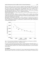
Fig. 7 shows measured spectral dependence of various kinds of photodiodes expressed in
spectral responsivity (a) and in spectral quantum efficiency (b). The detector having the
highest quantum efficiency of nearly unity is a silicon trap detector (Ichino, Y. et al., 2008),
which consists of three silicon photodiodes to reduce the overall reflection loss. The