Ultra Wideband Communications Novel Trends System, Architecture and Implementation Part 10 potx
Bạn đang xem bản rút gọn của tài liệu. Xem và tải ngay bản đầy đủ của tài liệu tại đây (1.72 MB, 25 trang )
Ultra Wideband Communications: Novel Trends – System, Architecture and Implementation
214
Fig. 1. Typical DC-RF efficiency for power amplifiers with a various bandwidth
For amplifier with W greater than 1.5:1 a high quality input matching and cascading of active
elements becomes problematic; here a balance circuit is widely used, in which two identical
active elements are connected with the help of 3-dB quadrature directional couplers while the
input reflections are fully absorbed by the ballast loads and a close to ideal input and output
matching is achieved (Sechi & Bujatti, 2009). In practice the balance amplifiers are used for
frequency coverage from 1.4:1 to 4:1 and have efficiency up to 25-45%.
To realize the frequency coverage over 4:1, most often a scheme of a distributed amplifier
(DA) is used, in which gates and drains of several transistors are united in artificial
transmission lines with a characteristic impendence close to 50 Ohm (Wong, 1993). The
lower working frequency of DA is limited only by DC-blocking circuits while the upper
frequency is determined by the upper frequencies of the input and output artificial lines and
depends on the transistor’s own capacitances. The DC-RF efficiency of DA is still lower
because of the difference of loads referred to individual transistors and redundancy of the
number of transistors used in the circuit. In practice W from 4:1 to over 1000:1 and efficiency
of 15-25% are achieved.
The qualitative ratios described above are applicable to amplifiers built on any types of
transistors (HBT, MESFET, MOSFET, HEMT). However, we shall go on considering
amplifiers on GaN HEMT transistors whose technology is rapidly developing and is taking
the first place by the combination of W-Ро-DE among the modern semiconductor
microwave frequency devices.
2. GaN transistors and MMIC technology
2.1 A short history
The history of invention and development of the GaN microwave transistors and MMICs
is rather short – a little less than 20 years from the moment of the first GaN-transistor
demonstration to the beginning of industrial devices implementation in electronic
Ultra-Wideband GaN Power Amplifiers - From Innovative Technology to Standard Products
215
systems. Of this period the first 10 to 15 years were devoted to the search for the best
transistor constructions and the ways for making them reliable and stable, while during
the next five years numerous efforts were directed to the industrial adoption of the
technology (Fig.2).
Fig. 2. The steps of GaN technology development history
This later stage was greatly promoted by a number of research programs financed by
military, governmental and corporate bodies of the USA, Japan and Europe. Among the one
should mention the Japanese program NEDO (Nanishi et al., 2006), the American DARPA
programs, called WBGS-RF and NEXT (Rosker et al., 2010), as well as the European
programs KORRIGAN, UltraGan, Hyphen, Great2 (Quay & Mikulla, 2010).
Early in the 2000s practically all the leading world electronic companies somewhat
connected with the production of GaAs-components begin making their own investments in
the GaN technology. These investments have given results and in the years 2006 and 2007
one watches announcing and then real appearance in the market of the first commercial
GaN-products: universal wideband transistors in the range of frequencies up to 2-4 ГГц
with the output CW power from 5 to 50 Watt (and somewhat later from 120 to 180 Watt).
The following companies have become the pioneers of the commercial market: Eudyna
(now Sumitomo Electric Devices Innovation, SEDI), Nitronex, Сree, and RFHIC. A little later
Toshiba, RF Microdevices (RFMD), TriQuint Semiconductor (TQ), and a number of other
companies have joined this first team.
In 2009 TriQuint began producing ultra-wideband MMIC amplifiers with the band of 2 to 17
GHz. By the end of 2010 GaN-based transistors and MMICs were already present in catalogs
of more than 15 companies – producers of semiconductor components from the USA,
Europe, Japan, South Korea, China and Russia.
2.2 Advantages
The interest of developers in GaN-transistors (or to be more precise in transistors on the
basis of heterostructures AlGaN/GaN) was due to combination of a number of important
material properties (Table 1).
Ultra Wideband Communications: Novel Trends – System, Architecture and Implementation
216
Properties Si AlGaAs
/InGaAs
SiC AlGaN
/GaN
Bandgap (E
g
), eV
1.1 1.4 3.2 3.4
Electron mobility (µ
n
), cm
2
V
-1
s-
1
1350 8500 700 1200-2000
Saturation field electron velocity (υ
sat
),
*10
7
cm/s
1.0 2.0 2.0 2.5
2D sheet electron density (n
s
), cm
-2
3 * 10
12
(1-2) * 10
13
Critical breakdown field (E
c
), MV/cm
0.3 0.4 2.0 3.3
Thermal conductivity (K), Wcm
-1
K
-1
1.5 0.5 4.5 1.3
Table 1. Basic properties of semiconductor materials for microwave power transistors
The maximum band-gap is determines the possibility of a transistor’s work at high levels of
activating influences (temperature and radiation). Very high electron density in the area of
two-dimentional electronic gas and a high saturation field electron velocity make possible
high channel current density and high transistor’s gain. The maximum critical breakdown
field allows realizing breakdown voltages of 100 to 300 V and increasing the working DC
voltage up to 50-100 V, which together with a high current density provides for power
density of industrial GaN transistors 4 to 8 W/mm (and up to 30 Watt/mm in laboratory
samples), which is ten times greater than the output power density of GaAs transistors. The
quality relations given in Fig.3 (Okumura, 2006) illustrate well the connection of the material
physical properties with the possible device output power density.
Fig. 3. Relations between the material physical properties and transistor power density
(Okumura, 2006)
The main power microwave transistors and MMIC technology well developed in the mass
production – the GaAs pseudomorphic HEMT technology (рНЕМТ) – is the main
competitor of the rapidly developing GaN technology. That is why further on we shall
compare parameters of transistors and MMICs having in mind these two technologies. For
estimating and comparing the application possibilities of GaN and GaAs transistors in the
wideband power amplifiers, as well as possible „migration“ of technical solutions from one
material to the other, let us make a simple analysis of their specific (i.e.related to 1 mm of the
Ultra-Wideband GaN Power Amplifiers - From Innovative Technology to Standard Products
217
gate width) parameters. Here was shall use the known (Cripps, 1999) estimations for the A
class amplifier with maximum output power Р
max
and optimal (for reaching such power)
transistor’s load resistance R
opt
:
Р
max
= V
ds
* I
max
/ 8 (1)
R
opt
= 2 * V
ds
/ I
max
(2)
where V
ds
is DC drain supply voltage, I
max
is maximum open channel current.
From the presented expressions one can easily receive a formula for a new parameter –
specific optimal load resistance (R
x
):
R
x
= V
ds
2
/ (4 * P
x
) (3)
where P
x
is a transistor’s output power density, which is the parameter that is widely used
in literature. The typical specific parameters of GaN HEMT and GaAs pНЕМТ transistors
received from the analysis of their linear equvivalent circuits given in literature and in
datasheets, as well as the above parameter R
x
are presented in Table 2.
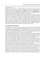
Parameters
GaAs
pHEMT
GaN
HEMT
typical TQ
TGF2022-
12
(1.2 mm)
typical TQ
TGF2023-
01
(1.25
mm)
Specific gate-source capacitance
(С
g
sx
), pF/mm
1.8 - 3 2.77 1.1 - 2 1.43
Specific transconductance (G
mx
),
mS/mm
200-400 313 150-300 216
Specific drain-source capacitance
(С
dsx
), pF/mm
0.15-0.3 0.19 0.2-0.4 0.246
Output power dencity (P
x
),
W/mm
0.7 1.0 5 4.5
Drain-source DC voltage (V
ds
), V 9 10 28 28
Specific optimal load (R
x
),
Ohm*mm
29 25 39 43.5
Power gain @ 10 GHz, dB 12.9 10.4
PAE @ 10 GHz, % 52.4 52
Output CW power @ 10 GHz,
Watt
1.2 5.5
Table 2. Absolute and specific transistor parameters comparison for GaAs and GaN
technologies
For comparison in this Table to as correct as possible we give specific parameters of two
industrial transistors produced by same company (TriQuint Semiconductor) and having
similar topologies, gate width and the equal gate length (0,25 μm).
The following conclusions can be drawn from the analysis of presented data:
Ultra Wideband Communications: Novel Trends – System, Architecture and Implementation
218
specific gate-surce capacitance and transconductance of GaN transistors
(simultaneously) are from 1.5 to 2 times as low as in GaAs transistors, which is more
likely the advantage of the former from the point of view of wideband input
matching, because it requires smaller transformation coefficients in matching circuits.
The achieved gain with the same gate-length may be considered to be sufficiently
close.
specific drain-source capacitance, that is shunting the optimal load of transistor and
making difficult the building of wideband output matching circuit at frequences that
are higher some cutt-off frequency, is in both classes of transistors almost the same.
specific optimal loads of transistor (R
x
) also turn out to be close (somewhat higher for
GaN-transistors).
2.3 “Technical solution migration”
The above considerations allow making a subtantiated assumption that many projects and
technical solutions as matching circuits or topology, worked out for GaAs-transistors and
MMICs, may with minimal changes be applied for GaN-transistors with the same or from
20% to 50% greater gate width. And if the gate length of booth types of active structures are
close, one can receive the same bandwidth, gain, and size of circuit, but with a several times
greater output power.
In the work (Fanning et al., 2005) there is description of rather a successful experiment on
„migration“ of standard GaAs pHEMT wideband power MMIC amplifier project (TGA9083
MMIC amplifier that have been manufactured for over 10 years by TriQuint Semiconductor)
to the GaN-on-Si technology, worked out by Nitronex Company. Frequency characteristics
of the saturated CW output power of two MMIC samples (GaAs pHEMT and GaN-on-Si
HEMT), assembled in a test circuit are shown in Fig.4, while the comparison of their
parameters is made in Table 3.
Fig. 4. Saturated output power of two MMIC amplifiers, manufactured according same
topology project on GaAs and on GaN-on-Si (Fanning et al., 2005)
Ultra-Wideband GaN Power Amplifiers - From Innovative Technology to Standard Products
219
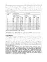
Parameters TGA9083
(GaAs
pHEMT)
New
(GaN-on-Si
HEMT)
Comments
Frequency range, GHz 6.5 - 11 7 – 10.5 =
Linear gain, dB (typ.) 19 20.9 =
Output CW power @ 3-dB gain
compression, W
8 20 x 2.5
PAE, % 35 27 =
Vd, V 9 24 x 2.7
Chip size, мм
2
4.5 х 3 =
Table 3. Comparison of parameters of two MMIC amplifiers, manufactured according same
topology project on GaAs and on GaN-on-Si (Fanning et al., 2005)
As one can see from the presented data a simple transfer of the complicated wideband
MMIC amplifier project onto a new technology gives considerable increase of the device
output power while the rest of the parameters remain preserved. A modification of this
project with a correct GaN transistor’s nonlinear model should further improve PAE and
output power of amplifier.
2.4 The ways for further improvement
The further improvement of the GaN transistor constructions is done in several directions.
First, it is the increase of the power density by raising break-down voltage, improving heat
removal, and increasing of efficiency. Second, is the frequency range extending into the
millimeter-wave frequencies with preservation of the power density and efficiency. Third, is
the lowering of production cost.
The increase of the transistor’s power density depends on the following:
by increasing the breakdown voltage (V
B
);
by lowering of transistor’s heat resistance by improvement thermal conductivity of the
substrate and optimization of transistor’s construction;
by increasing the maximum channel current (I
max
);
FP (Field Plate) electrode has become an effective way for increasing the breakdown voltage
that is successfully used in manufactured GaN transistors. This term is applied to a number
of transistor constructions. An additional electrode is located along the gate and it is
connected either with gate, or with source, or it is not connected with transistor electrodes at
all. This electrode allows changing the distribution of electric field in the channel, “moving
away” the peak of the field from the gate’s edge and “smoothing” it. This lows down the
gate leakage and increases the drain-source voltage when an avalanche ionization begins.
The constructions of FP electrodes used in GaN transistors are quite diverse. Two most
widespread ones are shown in Fig.5.
It is evident that the presence of an additional electrode, besides the increase of breakdown
voltage and output power density, causes other changes in the transistor characteristics as
well. In particular, there are significant changes in the cut-off frequencies F
t
и F
max
, and
parasitic capacitances of the active structure. Fig.6 shows relative changes of parameters of
GaN transistors with a FP electrode depending on the length of FP electrode L
f
. investigated
in the works (Kumar et al., 2006) and (Wu et al., 2004).
Ultra Wideband Communications: Novel Trends – System, Architecture and Implementation
220
(a) (b)
Fig. 5. Field-plated AlGaN/GaN HEMTs: (a) integrated field plate; (b) separated field plate
(Mishra, 2005)
Fig. 6. Deviations of basic transistor parameters with FP-electrode length (L
f
) variation
Inserting of the gate-connected FP electrode with L
f
= 1,1 um allowed increasing the
breakdown voltage from 68 to 110 volt and raising the output power density by 35%, from
5,4 to 7,3 Watt/mm. At the same time the current gain cut-off frequency decreased by 18%
to 20% (Kumar et al., 2006). This is probably conditioned by a considerable (two times)
increase of the parasitic capacitance Cgd (Wu et al., 2004). Transconductance and gate-
source capacitance of transistor after FP inserting have practically no any changes. The use
of a field electrode connected with the source of transistor, on the contrary, cuts down the
parasitic capacity Cgd and somewhat increases the cut-off frequencies and maximum
available (or stable) gain of transistor. The construction of such FP electrode is shown in
Fig.7 (Therrien et al., 2005).
Ultra-Wideband GaN Power Amplifiers - From Innovative Technology to Standard Products
221
Fig. 7. Cross section of AlGaN/GaN HEMT with source field plate (Therrien et al., 2005)
When such electrode was inserted (Therrien et al., 2005) transistor’s Cgd was decreased by
30%, while maximum stable gain (MSG) increased by 1,5 dB. Breakdown voltage also
increased significantly and there was also 1,5 times growth of output pulse power density
at Vd = 48 V. In the same way the insertion of a field electrode, connected with the source,
affected the parameters of transistor produced with the use of other technologies. In
particular, in GaAs MESFET transistor (Balzan et al., 2008) the capacity Cgd decreased by
43%, while the F
t
increased by 16%. In the SiC MESFET (Sriram et al., 2009) Cgd decreased
by 45% and MSG increased by 2, 7 dB.
The growth of output power density also leads to an increase of the heat dissipation on the
unit of the area of transistor’s active structure. If additional effortes are not taken, the
growth of channel temperature will limit the growth of transistor’s parameters and will lead
to the lowering of reliability. In modern GaN transistors the following materials and
composites are used (Table 4) as substrates on which the epitaxial layer of GaN is formed.
Substrate Thermal
conductivity,
W/ сm * К
Mono-crystalline SiC 4,9
High Resistive Si
(
111
)
1,5
Silicon on poly-crystalline
SiC (SopSiC)
3
Silicon on Diamond (SoD) 10-18
Table 4. Substrates for power GaN transistors
The mono-crystalline SiC substrate is the most often used material for industrial growing
epitaxial structures for GaN transistors. It is used by TriQuint Semicionductor, RFMD,
Toshiba, SEDI, Cree and a number of others. The production on substrates up to 100 mm
diameter was developed (Palmour et al., 2010). The technology using inexpensive substrates
of high-resistance silicon with intermediate buffer layers (GaN-on-Si) was developed by
Nitronex. TriQuint Semiconductor also plans to use this technology in future. Substrates of
SopSiC type, manufactured by method of transfer of the thin layer of high-resistance silicon
onto the poly-crystalline SiC substrate, are proposed for approbation by PicoGiga (PicoGiga
Ultra Wideband Communications: Novel Trends – System, Architecture and Implementation
222
International, 2011). In commercial production of transistors they are not used yet. Such
substrate must be cost-effective as compared to those from mono-crystalline SiC although
they are close to them in heat conductivity. A considerable progress in heat conductivity
may be expected from the use of composite substrates on the basis of poly-crystalline CVD
diamond developed by sp
3
Diamond Technologies (Zimmer & Chandler, 2007). The
proposed GaN transistor on SOD substrate cross-section is shown on Fig.8.
Fig. 8. Proposed GaN on SOD technology (Zimmer & Chandler, 2007)
Authors estimate that this technology will allow increasing the dissipated power of GaN
transistor by 50% as related to the mono-crystalline SiC.
The improvement of GaN transistor’s gain and extending of working frequencies into the
area of millimeter-waves are related with a search for new effective heterostructures that
would allow increasing electrons mobility, 2D sheet electron density, and, as a consequence,
increasing device’s transconductance, maximal open channel current, and cut-off
frequencies. These efforts are carried out in different fields. The achieved parameters of
some types of heterostructures (Wang et al., 2010, Sun et al., 2010, Jardel et al., 2010) in
comparison with the standard AlGaN/GaN structure are given in Table 5.
If the development of the above technologies are successful in industrial production,
parameters of GaN transistors and MMICs may be greatly improved already in the current
decade and will be characterized by the following figures (Table 6).
Parameters Heterostructures
Industry standard:
AlGaN/GaN
Innovative:
AlGaN/AlN/GaN,
AlInN/GaN,
InAlN/GaN …
Electron mobility
(cm
2
V
-1
s-
1
)
1000 - 1200 1400 - 2000
2D sheet electron density
(cm
-2
)
1 * 10
13
(1.4 – 2.0) * 10
13
Idss
(mA/mm) 500 - 1000 1300 - 2300
Gm
(mS/mm) 150 - 300 400 - 550
Table 5. Available GaN heterostructures parameters
Ultra-Wideband GaN Power Amplifiers - From Innovative Technology to Standard Products
223
Parameters Industry standard
2010
Industry standard
2015 - 2020
Power density (W/mm) 4 - 8 8 - 15
Gate length (um) 0.25 – 0.5 0.05 – 0.5
Frequency Range (GHz) 0 - 20 0 - 100
Output power (W/die) 5 - 100 5 - 200
Table 6. Available vs. today industry standard GaN transistors parameters
3. Manufacturing status
3.1 GaN discrete transistors
Discrete GaN transistors with the working frequencies up to S-band were historically first in
the microwave semiconductor market. Today they are produced with output CW power
from 5 to 200 Watt in different package types or in die form. The main parameters of the
commercially available devices is given in Table 7. There are data on three groups of
devices that are of interest as active elements for building UWB power amplifiers. The first
group («Low End») includes transistors with the output power of 5 to 12 Watt (this is the
minimal power level of the transistors produced today). They are supplied in die form or in
miniature SMD packages. On the basis of these transistors on can realize UWB amplifiers
with frequency coverage W from 3:1 to more than 100:1, because the maximum output
power is provided for with load impedance close to 50 Оhm (see Table 2) and the
possibilities for optimal output matching are limited in fact only by the construction of the
Parameters «Low End» (5W)
“High End Die”
(100W)
“High End Flange”
(200W)
Output CW Power (W) 5 - 12 100-120 180 - 220
Usable Upper
Frequency (GHz)
6 - 20 3-10 1.5 – 2.5
Available UWB ranges
(GHz)
0.1 - 3
1 – 6
3 – 10.5
4 - 12
0.8 – 2.5
1 – 3
2 - 4
0.5 – 1
1.0 – 1.5
Linear gain @ UF (dB) 12 - 15
Power gain @ UF (dB) 8 - 10
Drain Efficiency (%) 55-65
Packages SMD (4x4), Die Die Dual Flange
Some models
TQ TGF2023-01
TQ
T1G6000528Q3
Cree CGH40006Р
Cree CGH60008D
RFMD RF3930D
TQ TGF2023-20
Cree CGH60120D
RFMD RF3934D
Cree CGH40180PP
Nitronex NPT1007
SEDI
EGNB180M1A
Table 7. Discrete GaN HEMT main parameters
Ultra Wideband Communications: Novel Trends – System, Architecture and Implementation
224
drain DC bias circuit, which can be performed as a very wideband one. The maximum
working frequency for the amplifier based on discrete transistor with W greater than 3:1
may be estimated by the value of 12 GHz.
The maximum amplifier’s bandwidth may be realized by using transistors in die form
that have minimal parasitic gate and drain inductances. In our days there are GaN
transistors in die form with the gate width up to 28 mm and output CW power up to 120
Watt (“High End Die”). On the basis of these devices one can realize UWB amplifiers
with frequency coverage more than 3:1 on frequencies up to 4 GHz. Here the bandwidth
is limited by the difficulties of high-ratio impedance transformers realization to providing
for an optimal load at 3 or 4 Ohm with the parallel parasitic capacitance Cds being about 7
to 10 pF. The most powerful CW transistors (“High End Flange”) are produced in a
double flange ceramic packages, in which two separate transistors are located. They are
used in the amplifier either in accordance with the push-pull circuits, or in balanced
chains. The first one has an advantage that allows a 4 times increase of impedance of the
input and output matching circuits and provides for matching in a larger bandwidth. The
second circuits allows providing low input and output reflection coefficients and a good
matching with the driver and load. The most powerful industrial transistors of this class
have output CW power of up to 220 W. Because of significant package parasitic reactances
of such transistors the upper frequency of the wideband amplifier is seldom greater than
1.5 – 2 GHz.
3.2 UWB MMIC GaN amplifiers
Product mix of GaN MMIC power amplifiers is not yet great, but it is growing rapidly. UWB
microwave MMIC amplifiers are built in accordance with two main principals which we have
already mentioned above. This is a two- or three-stage circuit with reactive/dissipative
matching (RMA) and a distributed amplifier (DA). The balance circuits in GaN MMIC devices
is not widespread since the SiC substrate is cost-expensive, so using of quadrature couplers on
MMIC chip is not considered rational.
3.2.1 Distributed MMIC amplifiers
The greatest frequency coverage is provided for by the amplifier built on the principle of
distributed amplification, which is also called traveling-wave amplifier. The principle of
distributed amplification (Wong, 1993) has been used in electronics since the middle of
the last century and the epoch of vacuum-tube amplifiers. GaAs MMIC DA’s are
manufactured by dozens of companies. However, the output power and PAE of such
devices have already reached their full capacity. The appearance of GaN MMIC
technology has allowed making a considerable jump in the parameters of DA amplifiers.
In Table 8 we give parameters of the most powerful MMIC DA, realized by GaAs and
GaN technologies in the 2-18 GHz frequency range which is standard for such amplifiers
(and widely used for EW systems). Image of 2-18 GHz GaN MMIC DA with the output
CW power greater than 11 W, developed by specialists of TriQuint Semiconductor (Reese
et al., 2010) in the framework of stage III of WBGS-RF program is shown in Fig.9. As
compared to the most powerful commercially available GaAs DA this amplifier has 10
times as great output power, higher efficiency and 3,4 times greater die size. As a
commercially available only one type of GaN MMIC is so far known (TriQuint TGA2570)
with 8 W output power and 15-25% PAE. Improvement of parameters of heterostructure
Ultra-Wideband GaN Power Amplifiers - From Innovative Technology to Standard Products
225
and development of diamond-based substrates will allow increasing the 2-18 GHz MMIC
DA’s output power to the level of 20 to 30 W.
Parameters MMIC DA
2 – 18 GHz
GaAs GaN
Output CW Power (W) 1.0 – 1.2 11.0
PAE (%) 20 28
Linear gain (dB) 14 12
Vd (V) 10 35
Die size (mm
2
)
2.89 x 1.55 5.54 x 2.71
Model Hittite
Microwave
HMC797
(Reese et al.,
2010)
Table 8. GaN vs. GaAs MMIC distributed amplifier’s main parameters
Fig. 9. Photograph of the 2-18 GHz 11 Watt MMIC amplifier (Reese et al., 2010)
3.2.2 Reactive matched multistage MMIC amplifiers
The second solution that is often used for building MMIC amplifiers with frequency
coverage from 1.4:1 to 3:1 is a two- or three-stage circuit with a corporate reactive output
matching circuit and reactive/dissipative inter-stage and input matching circuits (RMA).
Today the majority of GaAs MMIC power amplifiers with the output power of over 1 or 2 W
have been built in accordance with this principle. This scheme has a better efficiency,
however it does not provide for a good input and inter-stage matching and, as a rule, it has
large gain ripple. And here also the appearance of GaN MMIC technology has allowed
making a considerable jump in parameters. In Table 9 we give main parameters of RMA-
amplifiers realized on GaAs and GaN technologies in the frequency ranges of 2-6 GHz and
6-18 GHz having frequency coverage of 3:1.
Ultra Wideband Communications: Novel Trends – System, Architecture and Implementation
226
Parameters MMIC RMA 2-6 GHz MMIC RMA 6 - 18 GHz
GaAs GaN GaAs GaN
Output CW Power (W) 10-12 22 - 35 2.5 - 3 6 - 10
PAE (%) 25 - 32 42 - 44 18 - 30 15 - 20
Linear gain (dB) 16 - 21 21 - 28 23 - 27 18 - 20
Vd (V) 10 28 8 25
Die size (mm
2
)
5.0 x 6.34 3.6 х 3.6 4.3 x 2.9 6.43 x 3.08
Model M/A Com
MAAPGM
0078-Die
Cree
CMPA20600
25D
TriQuint
TGA2501
(Mouginot et
al., 2010)
Table 9. GaN vs. GaAs MMIC reactively matched amplifier’s main parameters
On frequencies up to 6 GHz the advantages of GaN MMICs are considerably in all parameters:
the output power is 2.5-3 times higher, the efficiency is 1.5 times higher, and the die size is 2.5
times smaller. In the range from 6 to 18 GHz GaN MMIC has the output power 3 times as
great, but in the PAE and dimensions it is still inferior to GaAs amplifier. It should be noted
that GaN amplifier is one of the first models in the given class of MMIC, while the GaAs
amplifier has already been manufactured for 10 years. With improvement of technology,
nonlinear models of GaN transistors, and design methods GaN MMICs in this range will show
advantages in the efficiency as well. Image of the 2,5-6 GHz 30 W GaN MMIC amplifiers,
developed by the specialists of TriQuint Semiconductor (TGA2576) is shown in Fig.10.
Fig. 10. Photograph of the 2.5-6 GHz 30 Watt MMIC amplifier (www.triquint.com)
Improvement of hetero-structures parameters and mastering of diamond-based substrates
will allow increasing further the output power of MMIC RMA in the range from 2 to 6 GHz
up to the level of 50 to 60 W.
3.3 Commercially available GaN MMIC amplifiers
Parameters of some types of UWB MMIC amplifiers produced nowadays are given in Table
10. These MMICs cover the range of frequencies from 20 MHz to 17 GHz with the output
Ultra-Wideband GaN Power Amplifiers - From Innovative Technology to Standard Products
227
saturated power from 2 to 25-30 W. Among the manufactured MMICs only two types are
DA amplifiers, while in all the others the principle of reactive/dissipative matching is used.
All the UWB ranges with the output CW power from 10 to 30 Watt and DC-RF efficiency
from 20% to 50% are being overlapped by GaN MMIC amplifiers already in the third year of
manufacturing. Promotion of these devices in the market in future will depend on the
successes in the increase of production yield and lowering of prices as well as on the
“second jump” of the power density from 4-8 Watt/mm to 10-15 Watt/mm due to the
implementation of diamond-based substrates and improvement of transistor
heterostructures. The laboratory results of recent years (Micovic, 2008), that have
demonstrated the possibility of realizing MMIC amplifiers in the ranges up to 95 GHz with
the output power up to 0.5 Watt, will also be realized in commercially available MMICs.
Model Manu-
facturer
ΔF, GHz P
-3dB
,
W
G
ss
, dB ΔG,
±dB
PAE,
%
RL
in
,
dB
RL
out
,
dB
RFHA1000 RFMD 0,03-1,0 12-20 15 - 18 ±1.5 60 -13 -5
RF3833 RFMD 0,03-2,1 25 10-13 ±1.5 40-50 -9 -5
RF3826 RFMD 0,02-2,5 9 13 ±1.0 35-45 -10
TGA2540-FL TQ 0,03-3 9 19 40
CMPA0060002D
Cree 0,02 – 6,0 2-4 17 ±1.0 28-43 -9 -11
CMPA0060025F
Cree 0,02 – 6,0 25 16 - 21 ±3.0 26-40 -4 -7
CMPA2060025D
Cree 2.0-6.0 25 21 - 28 ±3.5 42-44 -7 -7
CMPA2560025F
Cree 2.5-6.0 25-37 22 - 28 ±3.0 > 30 -6 -5
TGA2576 TQ 2.5-6.0 35-45 20 - 23 ±1.5 > 35 -15 -6
CMPA801B025D Cree 8 - 11 32-47 27-30 ±1.5 37-44 -5 -12
TGA2570 TQ 2 - 17 8-12 10-12 ±2.0 20 -10 -10
Table 10. Some GaN power MMIC amplifiers parameters
4. High power GaN amplifier modules
Successes in the industrial development of GaN transistors and MMIC have immediately
found response in the efforts and results of the work of the developers of high power UWB
amplifier modules and systems. In 2009 through 2011 new devices appeared in the
catalogues of the majority of companies producing power amplifiers, which in their overall
mass parameters and the levels of CW output power surpass the earlier amplifiers on GaAs
components. The attraction of the discrete GaN transistors is conditioned by the following
considerations.
First. The scheme of the amplifier’s output stage, which provides for the main energy
consumption and dimensions, has been greatly simplified. To receive the required output
power one needs from 4 to 10 times less of the discrete or MMIC devices, power combiners,
and passive components. This cuts down the cost of the module construction and allows
making it much smaller in size. To illustrate the above we present in Fig.11 in the same scale
photographs of output stages of MIC broadband amplifiers with the output power of 10-15
Watt and the frequency range 4-11 GHz manufactured by Microwave Systems JSC on the
Ultra Wideband Communications: Novel Trends – System, Architecture and Implementation
228
basis of GaAs p-HEMT transistors (by combining the power of four balance quasi-
monolithic MIC amplifying chains) and on the basis of GaN HEMT transistors (one balance
MIC chain). The width of a module with GaN-based output stage has decreased three times
as compared with the variant on GaAs transistors with the same level of the output power.
Fig. 11. Output stages of 4-11 GHz 15 Watt MIC amplifiers based on GaAs and GaN
commercially available transistors – sizes and output CW power (Microwave Systems JSC)
The advantage in the size of the GaN modules may be estimated looking at Fig.12, where
photographs of two amplifiers produced by Empower RF Systems (www.empowerrf.com)
are given in the same scale. Both pictured models have the 50 W saturated output power in
the 1 to 3 GHz frequency range. GaAs-based model (BBM4A6AH5) have the volume of 71.8
inch
3
and weight of 5 lb, while the volume and the weight of the GaN-based model
(BBM4A6AHM) are correspondingly 23.9 inch
3
and 1.5 lb (the ratio here is 3:1).
Fig. 12. Comparison of sizes of 1-3 GHz 50W GaAs vs. GaN amplifier modules (Empower
RF Systems).
Second. With the appearance of GaN transistors the design methodology of the broadband
power amplifiers has been considerably simplified. High supply voltage and high
Ultra-Wideband GaN Power Amplifiers - From Innovative Technology to Standard Products
229
impedance of the optimal transistor load necessary for obtaining the maximum output
power and power-added efficiency make much simpler the construction of the output
matching circuits and improve the quality of matching in a much wider band of
frequencies.
Third. The use of GaN transistors allows increasing DC-RF efficiency of amplifiers. The
drain efficiency of GaN transistor itself biased in class AB without the use of special circuits
with harmonic reflections comprises from 60% to 65%, while in GaAs p-HEMT transistors it
is rarely over 55%. Due to this, as well as because here is a considerable decrease of losses in
the output combiners, DC-RF efficiency of GaN-amplifiers is as a rule from 1.2 to 1.8 times
greater than that in GaAs-amplifiers with the same power.
At the same time GaN amplifiers have specific features affecting their application in the
some systems. Primarily these are specificities of the dynamic characteristic having a
lengthy part of a monotonous gain compression with the growth of the input power, which
is not typical for GaAs amplifiers. The maximum output power and DE in GaN amplifiers
is realized with the gain compression from 3 to 7 or 8 dB and more, while in most GaAs
amplifiers the value of compression is not greater than 1 or 2 dB. Different characters have
also dependences of the harmonic level and intermodulation distortions from the input
power. Fig.13 gives dependences of the 2-tone output power and third order combination
components for two models of amplifiers having the same frequency range (from 2 to 4
GHz), the same maximum output CW power (25 W), and the same linear gain (43 dB), but
built on different types of transistors.
Fig. 13. Dynamic transfer characteristics and third-order intermodulation products of GaN
vs. GaAs 2-4 GHz 25W power amplifiers (Microwave Systems JSC)
The active introduction of GaN transistors and MMICs in the industry and the advantages
described above have led to the situation that during three years (from 2008 through 2010)
tens of UWB high power GaN amplifier modules have been put out into the market, while a
considerable part of the earlier GaAs amplifiers up to 3 GHz disappeared from the catalogs
of manufacturers due to harsh competition. The main characteristics of the most powerful
UWB GaN amplifiers that are being produced in 2011 are described in Table 11.
Ultra Wideband Communications: Novel Trends – System, Architecture and Implementation
230
Model Manufacturer ΔF, GHz P
sat
, W G
ss
,
dB
ΔG,
±dB
PAE,
%
Vdc,
V
BME2719-150 Comtech PST 0,02-1,0 150-200 70 - 35 18-36
BBM3T6AMQ Empower RF 0,96-3,0 160 56 ±2 30 28
BME19258-150 Comtech PST 1,0-2,5 250 70 25 18-36
SSPA-1,5-3,0-200 Aethercomm 1,5-3,0 200 67 ±2,5 25 36
BME25869-150 Comtech PST 2,5-6,0 150-200 65 18 18-36
BBM5A8CGM
Empower RF 2,0-6,0 40 55 ±1,5 15 28
PA020180-3932 Aeroflex 2,0-16,0 8 22 ±3,5 24 28
Table 11. UWB high power amplifiers parameters.
Thus, the area of radio frequencies from 20MHz to 6 GHz is occupied by module UWB
amplifiers on GaN transistors and MMICs with drain efficiency from 20% to 35% and the
output CW power up to 200 Watt. On the frequencies of over 6 GHz the level of the output
power of GaN amplifiers has so far been somewhat more modest; however there is no doubt
that in the nearest future in these ranges up to millimeter waves the models on GaAs will
partially be forced out from the market by devices on GaN.
5. Conclusion
This Chapter is devoted to consideration of the development process in the technology of
GaN microwave power transistors and MMICs and to demonstration of the prospects for
the development of this technology as an industrial standard in the nearest future. Electric
and exploitation parameters of GaAs and GaN technologies were compared with the
consideration of possible migration of power amplifier technical solutions from one to the
other. Considered and analyzed were also parameters and specific features of commercially
available GaN discrete transistors and MMICs, features of their application in constructions
of high power UWB amplifiers, and the parameters of industrial models of such amplifiers.
6. References
Colantonio P.; Giannini F. & Limiti E. (2009). High efficiency RF and microwave solid state power
amplifiers, John Wiley & Sons, 2009, ISBN: 978-0-470-51300-2
Sechi F. & Bujatti M. (2009). Solid-State Microwave High-Power Amplifiers, Artech House, 2009,
ISBN: 978-1-59693-319-4
Wong T.T.Y. (1993). Fundamentals of Distributed Amplifications, Artech House, 1993, ISBN: 0-
89006-615-9
Nanishi Y.; Miyamoto H; Suzuki A.; Okumura H. & Shibata M. (2006). Development of
AlGaN/GaN High Power and High Frequency HFETs under NEDO's Japanese
National Project, CS MANTECH Conference, 2006, p.p. 45-48
Rosker M.J.; Albrecht J.D.; Cohen E.; Hodiak J. & Chang T-H. (2010). DARPA’s GaN
Technology Thrust, 2010 IEEE MTT Symposium Digest, 2010, p.p. 1214-1217, ISSN:
978-1-4244-7732-6
Quay R. & Mikulla M. (2010). Gallium Nitride RF-Devices: An Overview on the
Development Activities in Europe, 2010 IEEE MTT Symposium Digest, 2010, p.p.
1234-1237, ISSN: 978-1-4244-7732-6
Ultra-Wideband GaN Power Amplifiers - From Innovative Technology to Standard Products
231
Okumura H. (2006). Present Status and Future Prospect of Widegap Semiconductor High-
Power Devices, Japanese Journal of Applied Physics, Vol. 45, No. 10A, 2006, pp. 7565–
7586
Cripps S.C. (1999). RF Power Amplifiers for Wireless Communications, Artech House, 1999,
ISBN: 0-89006-989-1
Fanning D.M.; Witkowski L.C.; Lee C.; Dumka D.C.; Tserng H.Q.; Saunier P.; Gaiewski W.;
Piner E.L.; Linthicum K.J. & Johnson J.W. (2005). 25 W X-band GaN on Si MMIC,
GaAs Mantech Conference Proceedings, 2005
Mishra U.K. (2005). Status of AlGaN/GaN HEMT Technology-A UCSB perspective, 13th
Gallium Arsenide and other Compound Semiconductors Application Symposium, 2005,
p.p. 21-28
Kumar V.; Chen G.; Guo S. & Adesida I. (2006). Field-Plated 0.25-μm Gate-Length
AlGaN/GaN HEMTs With Varying Field-Plate Length, IEEE Transactions on ED,
vol. 53, N 6, 2006, p.p. 1477-1480, ISSN: 0018-9383
Wu Y F.; Saxler A.; Moore M.; Wisleder T.; Chavarkar P.M. & Parikh P. (2004). Noise
Characteristics of Field-plated GaN HEMTs, 2004 Proceedings on IEEE Lester
Eastman Conference on High Performance Devices, p.p. 192-194, ISBN: 981-256-196
Therrien R.; Singhal S.; Johnson J.W.; Nagy W.; Borges R.; Chaudhari A.; Hanson A.W.;
Edwards A.; Marquart J.; Rajagopal P.; Park C.; Kizilyalli I.C. & Linthicum K.J.
(2005). A 36mm GaN-on-Si HFET Producing 368W at 60V with 70% Drain
Efficiency, 2005 IEEE International Electron Devices Meeting (IEDM), p.p. 568-571,
ISBN: 0-7803-9268
Balzan M.L.; Drinkwine M.J. & Winslow T.A. (2008). GaAs MESFET with Source-Connected
Field Plate for High Voltage MMICs, GaAs Mantech Conference Proceedings, 2008
Sriram S.; Hagleitner H.; Namishia D.; Alcorn T.; Smith T. & Pulz B. (2009). High-Gain SiC
MESFETs Using Source-Connected Field Plates, IEEE Electron Device Letters, vol.30,
2009, N 9, p.p. 952-953
Palmour J.W.; Hallin C.; Burk A.; Radulescu F.; Namishia D.; Hagleitner H.; Duc J.; Pribble
B.; Sheppard S.T,; Barner J.B. & Milligan J. (2010). 100 mm GaN-on-SiC RF MMIC
Technology, 2010 IEEE MTT Symposium Digest, 2010, p.p. 1226-1229, ISSN: 978-1-
4244-6057-1
PicoGiga International. (2011). GaN Thin Epiwafers for discrete power devices, RF &
microwave components, 16.03.2011, Available from
pdf/picogiga-gan-thin-epiwafers.pdf
Zimmer J. & Chandler G. (2007). GaN on SOD Substrates – The Next Step in Thermal
Control, CS MANTECH Conference, 2007, p.p. 129 – 132
Wang*H.; Chung J.W.; Gao X.; Guo S. & Palacios T. (2010). High Performance InAlN/GaN
HEMTs on SiC Substrate CS MANTECH Conference, 2010, p.p. 185-188
Sun H.; Alt A.R.; Benedickter H.; Feltin E.; Carlin J F.; Gonschorek M.; Grandjean N.R. &
Bolognesi C.R. (2010). 205-GHz (Al,In)N/GaN HEMTs, IEEE Electron Device Letters,
vol.31, 2010, N 9, p.p. 957-959
Reese E.; Allen D.; Lee C. & Nguyen T. (2010). Wideband Power Amplifier MMICs Utilizing
GaN on SiC, 2010 IEEE MTT Symposium Digest, 2010, p.p. 1230-1233, ISSN: 978-1-
4244-7732-6
Jardel O.; Callet G.; Dufraisse J.; Sarazin N.; Chartier E.; Reveyrand T.; Oualli M.; Lancereau
D.; Di Forte Poisson M.A.; Piotrowicz S.; Morvan E.; & Delage S.L. (2010).
Ultra Wideband Communications: Novel Trends – System, Architecture and Implementation
232
Performances of AlInN/GaN HEMTs for Power Applications at Microwave
Frequencies, Proceedings of the 5th European Microwave Integrated Circuits Conference,
2010, p.p. 49-52, ISSN: 978-2-87487-017-0
Micovic M.; Kurdoghlian A.; Moyer H.P.; Hashimoto P.; Hu M.: Antcliffe M.; Willadsen P.J.;
Wong W.S.; Bowen R.; Milosavljevic I.; Yoon Y.; Schmitz A.; Wetzel M.; McGuire
C.; HughesB. & Chow D.H. (2008). GaN MMIC PAs for E-Band (71 GHz – 95 GHz)
Radio, 30 th IEEE Compound Semiconductor IC (CSIC) Symposium, 2008
12
A Method for Improving Out-Of-Band
Characteristics of a Wideband Bandpass
Filter in an LTCC Substrate
Shinpei Oshima
1
, Koji Wada
2
, Ryuji Murata
1
and Yukihiro Shimakata
1
1
TAIYO YUDEN CO., LTD
2
The University of Electro-communications
Japan
1. Introduction
Recently, compact wireless modules using low temperature co-fired ceramic (LTCC)
technology are widely used for the wireless systems such as mobile phones, Bluetooth, and
wireless local-area networks(Lin et al.,2004; Wang et al.,2005). Fig.1 shows the general
structure of the compact wireless modules using the LTCC technology. The modules consist
of an LTCC substrate, integrated circuits, chip components, a shield, and passive
components embedded in the LTCC substrate (e.g., the bandpass filter, coupler and balun).
The embedded components in the LTCC substrate are fabricated by using the multilayer
structures based on thin ceramic sheets and conductor patterns. It becomes possible to
produce very compact modules compared to those with a general printed circuit board
substrate, because a number of passive components can be embedded in the substrate. To
adapt this technology for ultra wideband (UWB) wireless systems, a wideband bandpass
filter in the LTCC substrate is one of the most important technology because it decreases the
influences from other wireless systems. Various wideband bandpass filters have already
been presented(Ishida & Araki, 2004; Saitou et al.,2005; Li et al., 2005; Zhu et al.,2005; Horii
Fig. 1. A general structure of the compact wireless module using the LTCC technology.
Chip components
Integrated circuits
Shield
LTCC substrate
Bandpass filter, balun, coupler, et al.
Interconnections
Ultra Wideband Communications: Novel Trends – System, Architecture and Implementation
234
et al.,2006; Yamamoto et al.,2007; Shaman & Hong,2007; Tanii et al., 2008 ; Sun & Zhu, 2009).
However, these approaches cannot be easily applied for the embedded components in the
LTCC substrate. Therefore we have studied the compact wideband bandpass filters based
on the LTCC technology(Oshima et al.,2008; Oshima et al.,2010).
In this study, we propose a method for improving out-of-band characteristics of a wideband
bandpass filter. It is suitable for the compact UWB wireless modules using the LTCC
technology. The UWB systems assume the band group 1 (3.168-4.752GHz) of the multiband
orthogonal frequency-division multiplexing systems (Ghorashi et al., 2004).
Section 2 describes a wideband filter using the LTCC technology. We also point out that the
filter is desired to improve the attenuation characteristics. Section 3 explains a method for
improving out-of-band characteristics. In Section 4 and Section 5, we indicate the LTCC
structure of the presented filter, the simulated results, and the experimental results. Finally,
the conclusion of this study is summarized in Section 6.
2. Bandpass filter for UWB systems using the low-frequency band
Fig.2 shows the schematic of the wideband bandpass filter for UWB systems using the low-
frequency band (Oshima et al., 2010). Resonator 2 is the resonator which has a wide
passband and creates attenuation poles near the passband. Resonator 1 and Resonator 3 are
tap-feed resonators. The capacitors of C
2
and C
3
are coupling capacitors between the
resonators. The capacitors of C
4
and C
5
are used for the impedance matching and they also
improve out-of-band characteristics in the high-frequency region. The capacitor C
6
is used to
shorten the length of the strip line. In this study, the length of Resonator 3 differs from that
of Resonator 1 in order to create two attenuation poles at the high-frequency region. The
attenuation pole created by Resonator 1 is given by
AB
ABBA
jZ Z
0.
Z cot -Z tan
θθ
=
(1)
The attenuation pole created by Resonator 3 is also given by
EF
EFFE
jZ Z
0.
Z cot -Z tan
θθ
=
(2)
The attenuation poles created by Resonator 2 are given by
012
0 1 0 2
Y(Y-Y)
0
(Y + Y )(Y + Y )
=
(3)
where,
0
Y0.02=
(4)
1D D
1
DD
1-2 C Z tan
Y
j
Z tan
ωθ
θ
=
(5)
D3D
2
2
D3D D
jtan Y Z
Y
ZjYZ tan
θ
θ
+
=
+
(6)
A Method for Improving Out-Of-Band Characteristics
of a Wideband Bandpass Filter in an LTCC Substrate
235
6C C
3
C6CC
j
(CZ tan )
Y.
2Z (1- C Z tan )
ωθ
ωθ
+
=
(7)
The circuit parameters of the bandpass filter are decided by means of adjusting the
parameters in consideration of the conditions for the attenuation poles. This adjustment is
carried out by a commercial circuit simulator (ADS, Agilent Technologies, Inc.). Table 1
shows the parameters of the filter. Here, the reference frequency for the electrical length is
4.0 GHz. In this study, we use the physical strip line model in the circuit simulation because
this model can simulate the losses of the conductor and the LTCC substrate. Fig.3 shows the
physical strip line model. The relative permittivity of the LTCC substrate and the dielectric
loss tangent of the substrate are 7.1 and 0.005, respectively. The conductor in the substrate is
silver. Fig.4 indicates the results of the circuit simulation. The filter produces good
attenuation performances near the passband due to attenuation poles (f
1
and f
2
) which are
created by Resonator 2. The filter achieves good spurious suppression up to 10 GHz due to
the attenuation poles (f
3
and f
4
). They are created by Resonator 1 and Resonator 3. The input
impedance of the filter is also 50 ohm in the wide passband. However this filter is desired to
improve the attenuation characteristics because the filter cannot create a number of
attenuation poles at the frequency region lower than the passband and has the spurious
responses at the frequency band higher than 10 GHz .
Fig. 2. Schematic of the UWB bandpass filter for the low-frequency band.
Z
D
,
D
θ
C
1
Z
C
,
C
θ
C
6
C
4
C
2
C
5
C
3
Z
A
,
A
θ
Z
B
,
B
θ
Z
E
,
E
θ
Z
F
,
F
θ
Resonator 1
Resonator 2
Resonator 3
Port1
Port2
50 ohm50 ohm
Ultra Wideband Communications: Novel Trends – System, Architecture and Implementation
236
C
1
1.0pF Z
A
46.3 ohm
A
θ
43.9deg.
C
2
0.75pF Z
B
46.3 ohm
B
θ
26.9deg.
C
3
0.75pF Z
C
46.3 ohm
C
θ
50.9 deg.
C
4
0.5pF Z
D
38.6 ohm
D
θ
15.7deg.
C
5
0.5pF Z
E
46.3 ohm
E
θ
38.4 deg.
C
6
2.7pF Z
F
46.3 ohm
F
θ
26.9 deg.
Table 1. Parameters for the schematic shown in Fig.2.
Fig. 3. Physical model for a stripline.
Fig. 4. Simulated results of the filter shown in Fig.2.
LTCC
Relative permittivity : 7.1
350um
8um
005.0:tan
σ
Conductor (Silver)
Conductivity: 6.17X10
7
[S/m]
A Method for Improving Out-Of-Band Characteristics
of a Wideband Bandpass Filter in an LTCC Substrate
237
3. A method for improving out-of-band characteristics
In order to improve the spurious responses, the lowpass filter is very useful (Kurita & Li,
2007.). Fig.5 shows the schematic of the lowpass filter. This filter consists of a stripline and a
capacitor, which is suitable for the embedded components in the LTCC substrate (Ohwada
et al., 2002.). Fig.6 indicates the simulated results of the lowpass filter by the circuit
simulator. Where, Z
S
and
S
θ
are 46.3ohm and 33 deg.(@4GHz), respectively. In Case A, the
capacitor C
a
is 0.27 pF. In Case B, the capacitor is 0.34 pF. This lowpass filter can attenuate
the frequency region which is higher than 10 GHz. The attenuation characteristics of the
filter can be controlled by the value of the capacitor C
a
. However, the lowpass filter can not
attenuate the low-frequency band.
Fig. 5. Schematic of the lowpass filter.
Fig. 6. Simulated results of the lowpass filter shown in Fig.5.
Port1
Port2
Z
S
,
S
θ
C
a
50 ohm
50 ohm
Ultra Wideband Communications: Novel Trends – System, Architecture and Implementation
238
The input/output coupled filter can create attenuation poles (Shaman & Hong. 2007). It is
useful for improving the attenuation performances near the passband. However this filter
requires the quarter-wavelength coupled line and has the third harmonic.
For improving the out-of-band characteristics of the filter, we propose a method using
lowpass filters which consist of the coupling structure. Fig.7 shows the schematic of the
filter using the presented method. This circuit adds the lowpass filters at the input/output
ports of the filter shown in Fig.2. And a part of the stripline of the lowpass filters is the
coupling structure. Table 2 shows the parameters of the lowpass filters shown in Fig.7. In
Table 2, the reference frequency for the electrical length is 4.0 GHz. Z
So
and Z
Se
are odd- and
even-mode characteristic impedances. Fig.8 indicates the simulated results of the filter. We
can confirm that the filter has an additional attenuation pole (f
5
) at the low-frequency band
and suppresses the second and third harmonics. Fig.9 shows the characteristics of the filter,
when the coupling condition of the stripline is varied. It is confirmed that the attenuation
pole (f
5
) is controlled by the coupling stripline. This method uses the weak coupling
condition. Therefore it has little effect on the passband and the attenuation poles near the
passband. The filter keeps a high attenuation level in the high-frequency region. Note that
the locations of attenuation poles especially in the high-frequency region are varied by the
coupling condition.
Fig. 7. Schematic of the bandpass filter.
Port1
Port2
S1
θ
Z
S1
,
S3
θ
Z
So
,
S2
θ
Z
Se
,
Z
S1
,
C
a1
C
a2
Z
D
,
θ
C
1
Z
C
,
θ
C
6
C
4
C
2
C
5
C
3
Z
A
,
θ
Z
B
,
B
Z
E
,
Z
F
,
θ
A
C
E
θ
D
θ
F
50 ohm50 ohm