Wireless Sensor Networks Part 13 docx
Bạn đang xem bản rút gọn của tài liệu. Xem và tải ngay bản đầy đủ của tài liệu tại đây (3.24 MB, 25 trang )
Realizing a CMOS RF Transceiver for Wireless Sensor Networks 293
The analog front-end (AFE) of a realized WPAN receiver consists of continuous-time low
pass filters, highly linear programmable gain amplifier (PGA), filter tuning circuit, and DC
Gm Gm
Gm Gm
V
IP
V
con
V
IN
Vdd
Vss
V
OP
V
ON
Gm-cell
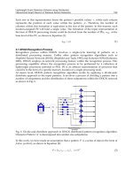
Fig. 4. Analog baseband circuits of receiver I: the channel selection filter with third-order
Butterworth LPF using proposed transconductance cells (Gm-cell)
offset cancellation block. The third order Butterworth filter was implemented cascading a
biquad cell and a single pole cell, and the programmable gain cell was stationed at the
middle to improve the cascaded dynamic range. The AFE design is concentrated on
optimizing the dynamic range and keeping the required die area small and low power
consumption. The baseband noise is dominated by the thermal noise of the PMOS current
sources at the quadrature mixer outputs. The flicker noise is not a significant problem at
baseband since all transistors are designed with a long channel length for better matching.
Moreover, the output of the DAC is DC blocked using a baseband modem control signal to
minimize the effect of the internal DC offsets from limiting the dynamic range of the
receiver.
The channel filter allows a signal of the desired band to pass and attenuates the adjacent
channel and the alternate channel. The filter requirement in this chapter, is
as follows. Since
it is a direct-conversion receiver (DCR) structure, 1/f noise should be reduced and the DC
offset should be small. In addition, in order to alleviate the SFDR requirements of the PGA
and the ADC, most of the interference is filtered in the first part (J. Silava-Martinez et al.
(1992), Y. Palaskas e al. (2004)). Figure 4 shows the designed third order Butterworth LPF.
Using the single pole of the passive RC at the output stage of the mixer reduces the
interference that can affect the dynamic range at the baseband input stage, and using the
overshoot of biquad compensates the in-band loss. Figure 4 shows the proposed Gm-cell
with degeneration resistor. Two Gm-cells are used as one to reduce the area that LPF
occupies. The lumped resistor and the size of MOS should be properly adjusted to improve
the linearity of the Gm-cell.
The signal level of the RF input requires a minimum dynamic range of 78 dB, namely from –
98 dBm to -20 dBm. The automatc gain-control (AGC) control signal receives the digital
control signal from the baseband modem to control the gain of the receiver. The PGA of this
receiver utilizes the three gain stages to control the gain of 0 ~ 65 dB with a 1-dB step. The
resistor switching method was utilized in order not to lose the linearity of PGA. I/Q 4bit
Fig. 5. Analog baseband circuits of receiver II: (a) The tuning circuit for channel selection
filter, (b) The circuit of a fusing cell for filter-tuning, (c) DAC schematic for DC offset
adjustment
dual flash-ADCs are designed for interface of baseband modem block. The simulated
maximum DC current consumption of an overall receiver path is 6 mA.
Figure 5 shows the automatic-tuning circuit, which is based on indirect tuning method.
Since the characteristics of the Gm-C filter are determined by the transconductance value,
the gm has to be controlled to keep a fixed pole frequency. The gm value should not be
changed even by process variations or outer environment changes. As shown in Fig. 5(a), it
is important to keep a gm value and a ratio of gm output current to gm input voltage equal.
And the required current for sinking or sourcing is designed to minimize changes of gm by
reducing current change due to the temperature variation from bias block. The current I1 in
Fig. 5(a) offsets the MOS of the bias part as well as the temperature variation of resistance so
as to minimize the changes of voltage Vab due to the temperature and to evenly maintain
the input voltage of the gm-cell. The converging time of tuning circuit is designed to less
than 100 msec. If the cut-off frequency differs from the designed value, as
a parameter set up
the first time it distorts the value of gm by the process variations, gm should be adjusted by
changing current I2 by fusing. Fusing is controlled by serial port
4
Fusing
Point
Zenb
dinb
PoR
do
I
M1
a
Vcm
R
R
I1
I1
Gm
C
CI2
I2
Vref1
Vref2
Up/
Dn
Cnt
Comparator
a
b
(a) (b)
d7
d0b
d1b
d2b
d3b
d4b
d5b
d6b
d0b
d7
d1b
d2b
d3b
d4b
d5b
d6b
d7b
d7b
Vcm
R
R
Iref
Vinp
Vinn
M1
M2 M3
M4 M5
P1 P2 P3
P4 P5
(c)
Wireless Sensor Networks 294
Fig. 6. Transmitter circuits: (a) Up-conversion I/Q-modulator using current-mixing scheme
(b) Drive-amplifier with off-chip inductor
interface (SPI), and there is no change in value once it is put in. Figure 5(b) represents the
circuit diagram of fusing cell. The fusing cell is a circuit which amplifies the voltage, which
is set in ratio of PMOS channel resistance to NMOS channel resistance within the range of
power on reset (‘Low’ PoR signal) at power-on. To inverting amplifier, the signal is latched
and displays the latched value without change while normal operation (‘High’ PoR signal).
The ‘Zenb’ is a signal of ‘fusing enable’, ‘dinb’ is a ‘data input signal’ controllable via SPI.
The ‘PoR’ is a signal for ‘enable’ at the mode of ‘power on reset’, while ‘do’ is an output
signal of fusing cell. Once the fusing signal turns to ‘enable’, the output signal of fusing cell
is fixed regardless of the data input signal. The current capacity of M1 should have more
than 1 mA in order to disconnect the node of a fusing point at transmitting the fusing enable
signal.
For DC offset adjustment, it is important for the cancellation of DC-offsets generated at the
back side of PGA1 and to use
the feedback loop to reduce the offset at the LPF output.
Figure 5(c) shows the DAC to convert the 8-bit data into the input voltage of the PGA. The
resolution for 1 bit is 5 mV, and the DC offset change at the LPF output is ±640 mV. The size
of MOS (P1~P5, M1~M5) used, as a current mirror of the DAC circuit has to be appropriate
in consideration of the current mismatch. The aspect ratio of the MOS is used by
20μm/2μm.
3.2 Transmitter
In the transmitter path, the BPSK modulated baseband signal is converted from digital to
analog before being applied to frequency up-translation block. Fig.6 (a) shows the schematic
of up-conversion mixer with RC low-pass filter. The baseband analog signal is filtered by
second RC low-pass filter, and then is translated into RF frequency by up-conversion
V
IN
V
IP
LO180
LO0
I
SS
/2
LO0
C
f
I
SS
/2
R
d
R
f
R
d
R
f
VDD
R
L
R
L
VSS
V
ON
V
OP
Pon
VDD
VSS
Pop
Vbias
Pip
Pin
L
off chip
On Chip
L
down bond
(a) (b)
modulator with balanced Gilbert-cell using current-mixing scheme. The major advantage of
current mixing relaxes a requirement of heavy linearity of modulator inputs from high
Fig. 7. Frequency synthesizer block-diagram with LC voltage-controlled oscillator
voltage-driving DAC output signal. In addition, this scheme for frequency-up modulation
can produce satisfactory results for high modulation quality, low-power consumption, and
good linearity. This balanced mixer converts baseband signal directly up to 900 MHz and
deliver -20 dBm differential signal to power amplifier. LO emission is due to differential
mismatch in the modulator circuit, while spectrum re-growth is due to LO (0/90-degree)
quardrature imbalance and nonlinearity of the Gilbert-cell. Layout is fulfilled very carefully
to maintain symmetry for differential and quardrature signals, which minimizes both LO
emission and spectrum re-growth. Fig.6 (b) shows the driver amplifier of a differential
common source topology with off-chip inductor having a high Q. The multiple down-bond
wire inductors are applied for the minimization of spectrum re-growth. The simulated DC
current consumption of an overall transmitter path is 7 mA.
3.3 Frequency Synthesizer
The integer-N frequency synthesizer, using a second-order passive loop filter, generates the
LO signal for transmit/receive mode. A crystal reference of 30 MHz is internally divided. To
minimize pulling, the 900-MHz LO signals are generated by 1.8 GHz voltage
controlled
oscillator (VCO), shown in Fig.7. The LC-resonator consists of four-turn spiral inductor and
varactor. The negative-Gm core cell has nMOS/pMOS complementary topology for high
power efficiency and gain.
1
2
OSC
eff
f
L
C
(1)
The oscillation frequency of VCO is shown as equation (1). The tuning frequency of VCO is
simulated from 1.6 GHz to 2.2 GHz. The divider circuit for high frequency has a structure of
negative-feedback type using two latches. The phase frequency detector (PFD) consists of
two D-flip-flop (DFF), AND-gate, and delay-time block for locking speed and high linearity
of phase transfer function. The charge-pump circuit has a structure of nMOS/pMOS
cascade-type to minimize of up/down current mismatch and output switching noise. The
clock generation block provides a reference clock of PLL and sampling-clocks of ADC/DAC
PFD CP
LF
Clock
Generator
[ 1/15 ]
Xtal
[30MHz]
[2MHz]
Fref.
[1.8GHz]
VCO
Off-chip
÷ 2
Divider
[P,S]=(56,5)
8/9
Prescaler
I/Q LO buffers
LO_I
LO_Q
Vop
Von
VDD
VSS
Vbias
Vc
LC-VCO
On-chip
Realizing a CMOS RF Transceiver for Wireless Sensor Networks 295
Fig. 6. Transmitter circuits: (a) Up-conversion I/Q-modulator using current-mixing scheme
(b) Drive-amplifier with off-chip inductor
interface (SPI), and there is no change in value once it is put in. Figure 5(b) represents the
circuit diagram of fusing cell. The fusing cell is a circuit which amplifies the voltage, which
is set in ratio of PMOS channel resistance to NMOS channel resistance within the range of
power on reset (‘Low’ PoR signal) at power-on. To inverting amplifier, the signal is latched
and displays the latched value without change while normal operation (‘High’ PoR signal).
The ‘Zenb’ is a signal of ‘fusing enable’, ‘dinb’ is a ‘data input signal’ controllable via SPI.
The ‘PoR’ is a signal for ‘enable’ at the mode of ‘power on reset’, while ‘do’ is an output
signal of fusing cell. Once the fusing signal turns to ‘enable’, the output signal of fusing cell
is fixed regardless of the data input signal. The current capacity of M1 should have more
than 1 mA in order to disconnect the node of a fusing point at transmitting the fusing enable
signal.
For DC offset adjustment, it is important for the cancellation of DC-offsets generated at the
back side of PGA1 and to use
the feedback loop to reduce the offset at the LPF output.
Figure 5(c) shows the DAC to convert the 8-bit data into the input voltage of the PGA. The
resolution for 1 bit is 5 mV, and the DC offset change at the LPF output is ±640 mV. The size
of MOS (P1~P5, M1~M5) used, as a current mirror of the DAC circuit has to be appropriate
in consideration of the current mismatch. The aspect ratio of the MOS is used by
20μm/2μm.
3.2 Transmitter
In the transmitter path, the BPSK modulated baseband signal is converted from digital to
analog before being applied to frequency up-translation block. Fig.6 (a) shows the schematic
of up-conversion mixer with RC low-pass filter. The baseband analog signal is filtered by
second RC low-pass filter, and then is translated into RF frequency by up-conversion
V
IN
V
IP
LO180
LO0
I
SS
/2
LO0
C
f
I
SS
/2
R
d
R
f
R
d
R
f
VDD
R
L
R
L
VSS
V
ON
V
OP
Pon
VDD
VSS
Pop
Vbias
Pip
Pin
L
off chip
On Chip
L
down bond
(a) (b)
modulator with balanced Gilbert-cell using current-mixing scheme. The major advantage of
current mixing relaxes a requirement of heavy linearity of modulator inputs from high
Fig. 7. Frequency synthesizer block-diagram with LC voltage-controlled oscillator
voltage-driving DAC output signal. In addition, this scheme for frequency-up modulation
can produce satisfactory results for high modulation quality, low-power consumption, and
good linearity. This balanced mixer converts baseband signal directly up to 900 MHz and
deliver -20 dBm differential signal to power amplifier. LO emission is due to differential
mismatch in the modulator circuit, while spectrum re-growth is due to LO (0/90-degree)
quardrature imbalance and nonlinearity of the Gilbert-cell. Layout is fulfilled very carefully
to maintain symmetry for differential and quardrature signals, which minimizes both LO
emission and spectrum re-growth. Fig.6 (b) shows the driver amplifier of a differential
common source topology with off-chip inductor having a high Q. The multiple down-bond
wire inductors are applied for the minimization of spectrum re-growth. The simulated DC
current consumption of an overall transmitter path is 7 mA.
3.3 Frequency Synthesizer
The integer-N frequency synthesizer, using a second-order passive loop filter, generates the
LO signal for transmit/receive mode. A crystal reference of 30 MHz is internally divided. To
minimize pulling, the 900-MHz LO signals are generated by 1.8 GHz voltage
controlled
oscillator (VCO), shown in Fig.7. The LC-resonator consists of four-turn spiral inductor and
varactor. The negative-Gm core cell has nMOS/pMOS complementary topology for high
power efficiency and gain.
1
2
OSC
eff
f
L
C
(1)
The oscillation frequency of VCO is shown as equation (1). The tuning frequency of VCO is
simulated from 1.6 GHz to 2.2 GHz. The divider circuit for high frequency has a structure of
negative-feedback type using two latches. The phase frequency detector (PFD) consists of
two D-flip-flop (DFF), AND-gate, and delay-time block for locking speed and high linearity
of phase transfer function. The charge-pump circuit has a structure of nMOS/pMOS
cascade-type to minimize of up/down current mismatch and output switching noise. The
clock generation block provides a reference clock of PLL and sampling-clocks of ADC/DAC
PFD CP
LF
Clock
Generator
[ 1/15 ]
Xtal
[30MHz]
[2MHz]
Fref.
[1.8GHz]
VCO
Off-chip
÷ 2
Divider
[P,S]=(56,5)
8/9
Prescaler
I/Q LO buffers
LO_I
LO_Q
Vop
Von
VDD
VSS
Vbias
Vc
LC-VCO
On-chip
Wireless Sensor Networks 296
using an external 30-MHz crystal-oscillator. The simulated DC current consumption of an
overall frequency synthesizer path is 8 mA.
Fig. 9. Measured results: (a) cascaded noise figure (NF), (b) cascaded IIP3 of overall receiver
4. Measured Results
Fig. 10. Measured result of spectrum mask of transmitter
SPI
RX
PLL
TX
Fig. 8. Die microphotograph
Frequency [MHz]
905 910 915 920 925
NF [dB]
8.0
8.5
9.0
9.5
10.0
10.5
11.0
RF Input Power [dBm]
-60 -50 -40 -30 -20 -10 0
Output Power [dBm]
-60
-40
-20
0
IIP3
(a) (b)
Fig. 11. Measured result of vector signal analysis of transmitter
A radio transceiver die microphotograph, which consists of transmitter, receiver, and
frequency synthesizer with on-chip VCO, is shown in Fig. 8. The total die area is 1.8 2.2-
mm
2
and it consumes only 29 mW in the transmit-mode, 25-mW in the receive-mode and a
LPCC48 package is used. The overall receiver features a cascaded-NF of 9.5 dB for 900 MHz
band as shown in Fig. 9(a). Overall receive cascaded- IIP
3
as shown in Fig. 9(b) is -10 dBm
and the maximum gain of receiver is 88dB. The automatic gain control (AGC) of receiver is
86dB with 1dB step and selectivity is -48 dBc at 5 MHz offset frequency. The 40 kHz
baseband single signal is up-converted by 906 MHz RF carrier signal and wanted-signals are
25dB higher than third-order harmonics. The spectrum density at the output of transmitter
satisfies the required spectrum mask as shown in Fig. 10, which is above 28 dBc at the ±1.2-
MHz offset frequency. Due to the low in-band integrated phase noise and the digital
calibration that eliminates I/Q mismatch and baseband filter mismatch, transmitter EVM is
dominated by nonlinearities (Behzad Razzavi (1997), I. Vassiliou et al. (2003), K. Vavelidis et
al. (2004)). As shown in Fig. 11, a reference design achieves 6.3 % EVM
for an output power
(a)
Realizing a CMOS RF Transceiver for Wireless Sensor Networks 297
using an external 30-MHz crystal-oscillator. The simulated DC current consumption of an
overall frequency synthesizer path is 8 mA.
Fig. 9. Measured results: (a) cascaded noise figure (NF), (b) cascaded IIP3 of overall receiver
4. Measured Results
Fig. 10. Measured result of spectrum mask of transmitter
SPI
RX
PLL
TX
Fig. 8. Die microphotograph
Frequency [MHz]
905 910 915 920 925
NF [dB]
8.0
8.5
9.0
9.5
10.0
10.5
11.0
RF Input Power [dBm]
-60 -50 -40 -30 -20 -10 0
Output Power [dBm]
-60
-40
-20
0
IIP3
(a) (b)
Fig. 11. Measured result of vector signal analysis of transmitter
A radio transceiver die microphotograph, which consists of transmitter, receiver, and
frequency synthesizer with on-chip VCO, is shown in Fig. 8. The total die area is 1.8 2.2-
mm
2
and it consumes only 29 mW in the transmit-mode, 25-mW in the receive-mode and a
LPCC48 package is used. The overall receiver features a cascaded-NF of 9.5 dB for 900 MHz
band as shown in Fig. 9(a). Overall receive cascaded- IIP
3
as shown in Fig. 9(b) is -10 dBm
and the maximum gain of receiver is 88dB. The automatic gain control (AGC) of receiver is
86dB with 1dB step and selectivity is -48 dBc at 5 MHz offset frequency. The 40 kHz
baseband single signal is up-converted by 906 MHz RF carrier signal and wanted-signals are
25dB higher than third-order harmonics. The spectrum density at the output of transmitter
satisfies the required spectrum mask as shown in Fig. 10, which is above 28 dBc at the ±1.2-
MHz offset frequency. Due to the low in-band integrated phase noise and the digital
calibration that eliminates I/Q mismatch and baseband filter mismatch, transmitter EVM is
dominated by nonlinearities (Behzad Razzavi (1997), I. Vassiliou et al. (2003), K. Vavelidis et
al. (2004)). As shown in Fig. 11, a reference design achieves 6.3 % EVM
for an output power
(a)
Wireless Sensor Networks 298
Frequency offset
100 Hz
1 MHz100 kHz10 kHz1 kHz
-110
-90
-130
-150
(b)
Fig. 12. Measured result of phase lock loop (PLL): (a) settling time, (b) phase noise
of –3dBm for sub-GHz ISM-band. Measured results of settling time and phase-noise plot of
phase locked loop
(PLL) are shown in Fig. 12. Table 1 summarizes the UHF RF transceiver’s
characteristics. The specifications of two RF transceivers (Walter Schucher et al. (2001)) and
(Hiroshi Komurasaki et al. (2003)) for UHF applications are also shown for comparison in
this table. The RX current is not the lowest; however, the power dissipation in RX mode is
the smallest because of the 1.8 V supply
voltage. Although the TX output power and RX IIP
3
are a little worse due to the antenna switch and the matching network, this work has great
advantages.
Specification This work
Walter Schucher et al.
(2001)
Hiroshi Komurasaki et
al. (2003)
VDD 1.8V 2.8V 1.8V
Current consum. Rx./Tx.:14/16mA Rx./Tx.: 11/20mA Rx./Tx.: 34/26mA
Die size 3.96 mm
2
10 mm
2
NF
9.5dB 11.8dB -76dBm
IIP
3
-10dBm -23.2dBm +3dBm
Max. Gain 88dB - -
AGC gain range 86 - -
Selectivity -48dBc (@5MHz) - -21dBc (@4MHz)
TX power +0dBm +10dBm +0dBm
EVM 6.3% - -
OP1-dB +1dBm - -
LO PN. (@1MHz) -108dBc -115dBc -
Table 1. The Measured Results of UHF Transceivers
5. Conclusion
A low power fully CMOS integrated RF transceiver chip for wireless sensor networks in
sub-GHz ISM-band applications is implemented and measured. The IC is fabricated in 0.18-
µm mixed-signal CMOS process and packaged in LPCC package. The fully monolithic
transceiver consists of a receiver, a transmitter and a RF synthesizer with on-chip VCO. The
overall receiver cascaded noise-figure, and cascade IIP
3
are 9.5 dB, and -10 dBm,
respectively. The overall transmitter achieves less than 6.3 % error vector magnitude (EVM)
for 40kbps mode. The chip uses 1.8V power supply and the current consumption is 25 mW
for reception mode and 29 mW for transmission mode. This chip fully supports the IEEE
802.15.4 WPAN standard in sub-GHz mode.
6. References
Behzad Razavi (1997). Design Considerations for Direct-Conversion, IEEE Transactions on
circuit and systems-II, 14, 251-260, June.
C. Cojocaru, T. Pamir, F. Balteanu, A. Namdar, D. Payer, I. Gheorghe, T. Lipan, K. Sheikh, J.
Pingot, H. Paananen, M. Littow, M. Cloutier, and E. MacRobbie (2003). A 43mW
Bluetooth transceiver with –91dBm sensitivity, ISSCC Dig. Tech. Papers, 90-91.
Hiroshi Komurasaki, Tomohiro Sano, Tetsuya Heima, Kazuya Yamamoto, Hideyuki
Wakada, Ikuo Yasui, Masayoshi Ono, Takahiro Miki, and Naoyuki Kato (2003). A
1.8 V Operation
RF CMOS Transceiver for 2.4 GHz Band GFSK Applications, IEEE
Journal of Solid-State Circuit, 38, May.
IEEE Computer Society (2003). IEEE Standard for Part 15.4: Wireless Medium Access
Control (MAC) and Physical Layer (PHY) specifications for Low Rate Wireless
Personal Area Networks (LR-WPANs), IEEE Standard 802.15.4TM.
Ilku Nam, Young Jin Kim, and Kwyro Lee (2003). Low 1/f Noise and DC offset RF mixer for
direct conversion receiver using parasitic vertical NPN bipolar transistor in deep
N-well CMOS Technology, IEEE symposium on VLSI circuits digest of technical.
I. Vassiliou, K. Vavelidis, T. Georgantas, S. Plevridis, N. Haralabidis, G. Kamoulakos, C.
Kapnistis, S. Kavadias, Y. Kokolakis, P. Merakos, J.C. Rudell, A. Yamanaka, S.
Bouras, and I. Bouras (2003). A single-chip digitally calibrated 5.15 GHz-5.825 GHz
0.18 μm CMOS
transceiver for 802.11a wireless LAN, IEEE J. Solid-State Circuits, 38,
2221–2231, December.
J. Bouras, S. Bouras, T. Georgantas, N. Haralabidis, G. Kamoulakos, C. Kapnistis, S.
Kavadias, Y. Kokolakis, P. Merakos, J. Rudell, S. Plevridis, I. Vassiliou, K. Vavelidis,
and A. Yamanaka (2003). A digitally calibrated 5.15– 5.825 GHz transceiver for
802.11a wireless LANS in 0.18 μm
CMOS, IEEE Int. Solid-State Conf. Dig.Tech.
Papers, February.
J. Silva-Martinez, M.S.J. Steyaert, and W. Sansen (1992). A 10.7 MHz, 68 dB
SNR CMOS
Continuous-Time Filter with On-Chip Automatic Tunig, IEEE J. Solid-State
Circuits, 27, 1843-1853, December.
Kwang-Jin Koh, Mun-Yang Park, Cheon-Soo Kim, and Hyun-Kyu Yu (2004).
Subharmonically Pumped CMOS Frequency Conversion (Up and Down) Circuits
For 2 GHz WCDMA
Direct-Conversion Transceiver, IEEE J. Solid-State Circuits, 39,
871-884, June.
K. Vavelidis, I. Vassiliou, T. Georgantas, A. Yamanaka, S. Kavadias, G. Kamoulakos, C.
Kapnistis, Y. Kokolakis, A. Kyranas, P. Merakos, I. Bouras, S. Bouras, S. Plevridis,
and N. Haralabidis (2004). A dual- band 5.15-5.35 GHz, 2.4-2.5 GHz 0.18 μm CMOS
Transceiver for 802.11a/b/g wireless LAN, IEEE J. Solid-State Circuits, 39, 1180-
1185, July.
Realizing a CMOS RF Transceiver for Wireless Sensor Networks 299
Frequency offset
100 Hz
1 MHz100 kHz10 kHz1 kHz
-110
-90
-130
-150
(b)
Fig. 12. Measured result of phase lock loop (PLL): (a) settling time, (b) phase noise
of –3dBm for sub-GHz ISM-band. Measured results of settling time and phase-noise plot of
phase locked loop
(PLL) are shown in Fig. 12. Table 1 summarizes the UHF RF transceiver’s
characteristics. The specifications of two RF transceivers (Walter Schucher et al. (2001)) and
(Hiroshi Komurasaki et al. (2003)) for UHF applications are also shown for comparison in
this table. The RX current is not the lowest; however, the power dissipation in RX mode is
the smallest because of the 1.8 V supply
voltage. Although the TX output power and RX IIP
3
are a little worse due to the antenna switch and the matching network, this work has great
advantages.
Specification This work
Walter Schucher et al.
(2001)
Hiroshi Komurasaki et
al. (2003)
VDD 1.8V 2.8V 1.8V
Current consum. Rx./Tx.:14/16mA Rx./Tx.: 11/20mA Rx./Tx.: 34/26mA
Die size 3.96 mm
2
10 mm
2
NF
9.5dB 11.8dB -76dBm
IIP
3
-10dBm -23.2dBm +3dBm
Max. Gain 88dB - -
AGC gain range 86 - -
Selectivity -48dBc (@5MHz) - -21dBc (@4MHz)
TX power +0dBm +10dBm +0dBm
EVM 6.3% - -
OP1-dB +1dBm - -
LO PN. (@1MHz) -108dBc -115dBc -
Table 1. The Measured Results of UHF Transceivers
5. Conclusion
A low power fully CMOS integrated RF transceiver chip for wireless sensor networks in
sub-GHz ISM-band applications is implemented and measured. The IC is fabricated in 0.18-
µm mixed-signal CMOS process and packaged in LPCC package. The fully monolithic
transceiver consists of a receiver, a transmitter and a RF synthesizer with on-chip VCO. The
overall receiver cascaded noise-figure, and cascade IIP
3
are 9.5 dB, and -10 dBm,
respectively. The overall transmitter achieves less than 6.3 % error vector magnitude (EVM)
for 40kbps mode. The chip uses 1.8V power supply and the current consumption is 25 mW
for reception mode and 29 mW for transmission mode. This chip fully supports the IEEE
802.15.4 WPAN standard in sub-GHz mode.
6. References
Behzad Razavi (1997). Design Considerations for Direct-Conversion, IEEE Transactions on
circuit and systems-II, 14, 251-260, June.
C. Cojocaru, T. Pamir, F. Balteanu, A. Namdar, D. Payer, I. Gheorghe, T. Lipan, K. Sheikh, J.
Pingot, H. Paananen, M. Littow, M. Cloutier, and E. MacRobbie (2003). A 43mW
Bluetooth transceiver with –91dBm sensitivity, ISSCC Dig. Tech. Papers, 90-91.
Hiroshi Komurasaki, Tomohiro Sano, Tetsuya Heima, Kazuya Yamamoto, Hideyuki
Wakada, Ikuo Yasui, Masayoshi Ono, Takahiro Miki, and Naoyuki Kato (2003). A
1.8 V Operation
RF CMOS Transceiver for 2.4 GHz Band GFSK Applications, IEEE
Journal of Solid-State Circuit, 38, May.
IEEE Computer Society (2003). IEEE Standard for Part 15.4: Wireless Medium Access
Control (MAC) and Physical Layer (PHY) specifications for Low Rate Wireless
Personal Area Networks (LR-WPANs), IEEE Standard 802.15.4TM.
Ilku Nam, Young Jin Kim, and Kwyro Lee (2003). Low 1/f Noise and DC offset RF mixer for
direct conversion receiver using parasitic vertical NPN bipolar transistor in deep
N-well CMOS Technology, IEEE symposium on VLSI circuits digest of technical.
I. Vassiliou, K. Vavelidis, T. Georgantas, S. Plevridis, N. Haralabidis, G. Kamoulakos, C.
Kapnistis, S. Kavadias, Y. Kokolakis, P. Merakos, J.C. Rudell, A. Yamanaka, S.
Bouras, and I. Bouras (2003). A single-chip digitally calibrated 5.15 GHz-5.825 GHz
0.18 μm CMOS
transceiver for 802.11a wireless LAN, IEEE J. Solid-State Circuits, 38,
2221–2231, December.
J. Bouras, S. Bouras, T. Georgantas, N. Haralabidis, G. Kamoulakos, C. Kapnistis, S.
Kavadias, Y. Kokolakis, P. Merakos, J. Rudell, S. Plevridis, I. Vassiliou, K. Vavelidis,
and A. Yamanaka (2003). A digitally calibrated 5.15– 5.825 GHz transceiver for
802.11a wireless LANS in 0.18 μm
CMOS, IEEE Int. Solid-State Conf. Dig.Tech.
Papers, February.
J. Silva-Martinez, M.S.J. Steyaert, and W. Sansen (1992). A 10.7 MHz, 68 dB
SNR CMOS
Continuous-Time Filter with On-Chip Automatic Tunig, IEEE J. Solid-State
Circuits, 27, 1843-1853, December.
Kwang-Jin Koh, Mun-Yang Park, Cheon-Soo Kim, and Hyun-Kyu Yu (2004).
Subharmonically Pumped CMOS Frequency Conversion (Up and Down) Circuits
For 2 GHz WCDMA
Direct-Conversion Transceiver, IEEE J. Solid-State Circuits, 39,
871-884, June.
K. Vavelidis, I. Vassiliou, T. Georgantas, A. Yamanaka, S. Kavadias, G. Kamoulakos, C.
Kapnistis, Y. Kokolakis, A. Kyranas, P. Merakos, I. Bouras, S. Bouras, S. Plevridis,
and N. Haralabidis (2004). A dual- band 5.15-5.35 GHz, 2.4-2.5 GHz 0.18 μm CMOS
Transceiver for 802.11a/b/g wireless LAN, IEEE J. Solid-State Circuits, 39, 1180-
1185, July.
Wireless Sensor Networks 300
M. Zargari, M. Terrovitis, S.H.M. Jen, B.J. Kaczynski, MeeLan Lee, M.P. Mack, S.S. Mehta, S.
Mendis, K. Onodera, H. Samavati, W.W. Si, K. Singh, A. Tabatabaei, D. Weber, D.K.
Su, and B.A. Wooley (2004). A Single-Chip Dual-Band Tri-Mode CMOS Transceiver
for IEEE 802.11a/b/g Wireless LAN”, IEEE J. Solid-State Circuits, 39, 2239-2249,
December.
M. Valla, G. Montagna, R. Castello, R. Tonietto, and I. Bietti (2005). A 72 mW CMOS 802.11a
Direct Conversion Front-End with 3.5 dB NF and 200 kHz 1/f Noise Corner, IEEE J.
Solid-State Circuits, 40, 970-977, April.
Pengfei Zhang, T. Nguyen, C. Lam, D. Gambetta, T. Soorapanth, Baohong Cheng, S. Hart, I.
Sever, T. Bourdi, A. Tham, and B. Razavi (2003). “A 5 GHz Direct-Conversion
CMOS Transceiver” IEEE Journal of Solid-State Circuit, 38, December.
P. S. Choi, H. C. Park, S. Y. Kim, S. C. Park, I. K. Nam, T. W. Kim, S. J. Park, S. H. Shin, M. S.
Kim, K. C. Kang, Y. W. Ku; H. J. Choi, S. M. Park, and K. R. Lee (2003). “An
Experimental Coin-Sized Radio for Extremely Low-Power WPAN Application at
2.4GHz,” IEEE J. Solid-State Circuits, 12, 2258-2268, December.
S.F.R. Chang, Wen-Lin Chen, Shuen-Chien Chang, Chi-Kang Tu, Chang-Lin Wei, Chih-
Hung Chien, Cheng-Hua Tsai, J. Chen, and A. Chen (2005), A Dual-Band RF
Transceiver for Multistandard WLAN Applications. IEEE Transaction on
Microwave Theory and Techniques, 53, 1040-1055, March.
S. Sarkar, P. Sen, A. Raghavan, S. Chakarborty, and J. Laskar (2003). Development of 2.4
GHz RF Transceiver Front-end Chipset in 0.25µm CMOS, Proceedings of the 16
th
International Conference on VLSI Design.
Walter Schuchter, Guenter Krasser, and Guenter Hofer (2001). A Single Chip FSK/ASK
900MHz Transceiver in a Standard 0.25um CMOS Technology, IEEE RFIC
Symposium.
W. Hioe, K. Maio, T. Oshima, Y. Shibahara, T. Doi, K. Ozaki, and S. Arayashiki, “0.18-um
CMOS Bluetooth Analog Receiver With 88-dBm Sensitivity (2004). IEEE J. Solid-
State Circuits, 39, 374-377, February.
Y. J. Jung, H. S. Jeong, E. S. Song, J. H. Lee, S. W. Lee, D. Y. Seo, I. H. Song, S. H. Jung, J. B.
Park, D. K. Jeong, S. I. Chae, and W. Kim (2004). A 2.4-GHz 0.25um CMOS dual-
mode direct-conversion transceiver for bluetooth and 802.11b, IEEE Journal of
solid-state circuits, 39, July
Y. K. Park, H. M. Seo, Y. K. Moon, K. H. Won, and S. D. Kim (2005). Low Power Radio
Receiver Specifications of Ubiquitous System for Coexistence with Various Wireless
Devices in 2.4GHz ISM-band, The 20th International Technical Conference on
Circuits/System, Computers and Communications, July.
Y. Palaskas, Y. Tsividis, V. Prodanov, and V. Boccuzzi (2004). A Divide and Conquer
Technique for Implementing Wide Dynamic Range Continuous-Time Filters, IEEE J.
Solid-State Circuits, 39, 297-307, February.
Wireless Sensor Networks and Their Applications to the Healthcare and Precision Agriculture 301
Wireless Sensor Networks and Their Applications to the Healthcare and
Precision Agriculture
Jzau-Sheng Lin, Yi-Ying Chang, Chun-Zu Liu and Kuo-Wen Pan
X
Wireless Sensor Networks and Their
Applications to the Healthcare
and Precision Agriculture
Jzau-Sheng Lin
*
, Yi-Ying Chang
*
, Chun-Zu Liu
**
and Kuo-Wen Pan
**
*
Department of Computer Science and Information Engineering,
**
Institute of Electronics Engineering
National Chin-Yi University of Technology, Taichung, Taiwan, R.O.C.
Abstract
Wireless connection based smart sensors network can combine sensing, computation, and
communication into a single, small device. Because sensor carries its own wireless data
transceiver, the time and the cost for construction, maintenance, the size and weight of
whole system have been reduced. Information collected from these sensor nodes is routed to
a sink node via different types of wireless communication approaches.
Healthcare systems have restricted the activity area of patients to be within the medical
health care center or residence area. To provide more a feasible situation for patients, it is
necessary to embed wireless communication technology into healthcare systems. The
physiological signals are then immediately transmitted to a remote management center for
analysis using wireless local area network. Healthcare service has been further extended to
become mobile care service due to the ubiquity of global systems for mobile
communications and general packet radio service.
It is important that using sensors to detect field-environment signals in agriculture is
understood since a long time ago. Precision agriculture is a technique of management of
large fields in order to consider the spatial and temporal variability. To use more
sophisticated sensor devices with capabilities of chemical and biological sensing not only
aids the personnel in the field maintenance procedure but also significantly increases the
quality of the agricultural product.
In this chapter, we examine the fields in healthcare and precision agriculture based on
wireless sensor networks. In the application of healthcare systems, a System on a Chip (SoC)
platform and Bluetooth wireless network technologies were combined to construct a
wireless network physiological signal monitoring system. In the application of precision
agriculture, an SoC platform was also used combining the ZigBee technology to consist a
field signals monitoring system. In addition to the two applications, the fault tolerance in
wireless sensor networks is also discussed in this chapter.
Keywords: wireless sensor networks; healthcare; precision agriculture; Bluetooth; ZigBee.
15
Wireless Sensor Networks 302
1. Introduction to the wireless sensor networks
Owing to the rapid development of new medicines and medical technologies, the aged
population have been resulted in a speed-up increase. Thus, more rehabilitation centers are
created for the requirements of homecare as well as more medical personnel is needed to
offer medical treatments and to prevent accidents for aged patients. To provide a more
humane environment for these aged patients’ physical and physiological heath care,
monitoring and recording of their physiological status is very important [1-16]. It occupies a
large portion of center’s human resources to regularly observe and record the physiological
status of patients. It still cannot guarantee to obtain the necessary patients’ status
information on time and to prevent accidents from happening even if we have sufficient
professional nursing staff who works very carefully. In order to reduce the nursing staff’s
loading and prevent sudden situations that cause accidents, a physiological signal acquiring
and monitoring system for the staff to collect the physiological status information of patients
to the nursing center with physiological sensors module is essential.
Several technologies were used in the precision agriculture such as remote sensing, global
positioning system (GPS), geographic information system (GIS), microelectronics and
wireless communications [17, 18]. Most GPS and GIS with satellite systems provide images
of great areas. Alternatively wireless sensor networks (WSNs), used for precision agriculture,
give better spatial and temporal variability than satellites, in addition to permit collection of
others soil and plant data, as temperature, moisture, pH, and soil electrical conductivity [19,
20].
Currently three main wireless standards are used namely WiFi, Bluetooth and ZigBee,
respectively. Wi-Fi networks, a standard named IEEE 802.11, is a radio technology to
provide reliable, secure, fast wireless connectivity. A Wi-Fi network can be used to connect
computers to each other, to the Internet, and to wire networks. Wi-Fi networks work in the
unlicensed 2.4 GHz and 5 GHz radio bands, with a data rate of 11 Mbit/s or 54 Mbit/s. They
can provide real-world performance similar to that of the basic 10BASE-T wired Ethernet
networks. Unlike a wired Ethernet, Wi-Fi cannot detect collisions, and instead uses an
acknowledgment packet for every data packet sent.
Bluetooth is a protocol for the use of low-power radio communications over short distance
to wirelessly link phones, computers and other network devices. Bluetooth technology was
designed to support simple wireless networking of personal consumer devices and
peripherals, including PDAs, cell phones, and wireless headsets. Wireless signals
transmitted with Bluetooth cover short distances, typically up to 10 meters. Bluetooth
devices generally communicate at less than 1 M bps in data transmission. The wireless
Bluetooth technology is popularly used in several technique fields. Many researchers have
used Bluetooth technology to their monitoring system [12]. Wireless mobile monitoring
systems for physiological signal not only increase the mobility of uses but also improve the
quality of health care [13].
ZigBee is a low-power, low-cost, wireless mesh networking standard. The low power allows
longer life with smaller batteries, the low cost allows the technology to be widely developed
in wireless control and monitoring applications and the mesh networking provides high
dependability and larger range. ZigBee operates in the industrial, scientific and medical
radio bands with 868 MHz, 915 MHz, and 2.4 GHz in different countries. The technology is
intended to be simpler and less expensive than other WPANs such as Bluetooth.
Of those, ZigBee is the most promising standard owing to its low power consumption and
simple networking configuration. The prospective benefits of using the WSN technologies in
agriculture resulted in the appearance of a large number of R&D projects in this application
domain. The job of the sensor network in this Chapter is to provide constant monitoring of
field-environment factors in an automatic manner and dynamic transmitting the measured
data to the farmer or researchers with WSN based on Zigbee and Internet. The real time
information from the fields will provide a solid base for farmers to adjust strategies at any
time.
Beside to develop a low cost, high performance and flexible distributed monitoring system
with an increased functionality, the main goal of this chapter is to use a fault detection
algorithm to detect fault sensing nodes in the region of fields. In the proposed strategy,
wireless sensors send data via a Microprocessor Control Unit (MCU) and a wireless-based
transmitter. The receiver unit receives data from a receiver and an SoC platform. And, these
data are transmitted to the Internet through the RJ-45 connector. A remote data server stores
the data. Any web browser, smart phone or PC terminal with access permission can view
the data and remotely control the wireless network.
The rest of this chapter is organized as follows. Section 2 introduces the application to the
healthcare technology, in which the system architecture of the monitoring system for the
physiological signals including wireless-network acquiring unit and receiver unit with an
SOC platform are discussed; The detail circuit of wireless-network acquiring unit and
receiver unit for the application to the precision agriculture are mentioned in Section 3; The
application scenario for the ZigBee based networks were demonstrated in Section 4; Section
5 describes the fault tolerance in WSN to detect the fault sensing nodes; Finally, the
conclusions and the future work are indicated in Chapter 6.
2. The Application to the Healthcare technology
This Section proposed a wireless network physiological signal monitoring system which
integrates an SoC platform and Bluetooth wireless network technologies in homecare
technology. The system is constituted by three parts which include mobile sensing unit,
Bluetooth module and web-site monitor unit. Firstly we use acquisition sensors for
physiological signals, an MCU as the front-end processing device, and several filter and
amplifier circuits to process and convert signals of electrocardiogram (ECG), body
temperature and heart rate into digital data. Secondly, Bluetooth module was used to
transmit digital data to the SoC platform with wireless manner. Finally, an SoC platform, as
a Web server additionally, to calculate the value of ECG, the values of body temperature
and the heart rate. Then, we created a system in which physiological signal values are
displayed on Web page or collected into nursing center in real-time through RJ-45 of an SoC
platform. The results show our proposed wireless network physiological signal monitoring
system is very feasible for future applications in homecare technology.
Because of the fast development and wide application of Internet, homecare applications to
provide health monitoring and care by sending personal physiological signals to Internet
have become highly feasible. However, the health care systems have restricted the activity
area of patients to be within medical health care center or within residence area. To provide
more feasible manner for patients, it is necessary to embed wireless communication
technology into healthcare systems. The physiological signals are then immediately
transmitted to a remote management center for analysis by using wireless local area
Wireless Sensor Networks and Their Applications to the Healthcare and Precision Agriculture 303
1. Introduction to the wireless sensor networks
Owing to the rapid development of new medicines and medical technologies, the aged
population have been resulted in a speed-up increase. Thus, more rehabilitation centers are
created for the requirements of homecare as well as more medical personnel is needed to
offer medical treatments and to prevent accidents for aged patients. To provide a more
humane environment for these aged patients’ physical and physiological heath care,
monitoring and recording of their physiological status is very important [1-16]. It occupies a
large portion of center’s human resources to regularly observe and record the physiological
status of patients. It still cannot guarantee to obtain the necessary patients’ status
information on time and to prevent accidents from happening even if we have sufficient
professional nursing staff who works very carefully. In order to reduce the nursing staff’s
loading and prevent sudden situations that cause accidents, a physiological signal acquiring
and monitoring system for the staff to collect the physiological status information of patients
to the nursing center with physiological sensors module is essential.
Several technologies were used in the precision agriculture such as remote sensing, global
positioning system (GPS), geographic information system (GIS), microelectronics and
wireless communications [17, 18]. Most GPS and GIS with satellite systems provide images
of great areas. Alternatively wireless sensor networks (WSNs), used for precision agriculture,
give better spatial and temporal variability than satellites, in addition to permit collection of
others soil and plant data, as temperature, moisture, pH, and soil electrical conductivity [19,
20].
Currently three main wireless standards are used namely WiFi, Bluetooth and ZigBee,
respectively. Wi-Fi networks, a standard named IEEE 802.11, is a radio technology to
provide reliable, secure, fast wireless connectivity. A Wi-Fi network can be used to connect
computers to each other, to the Internet, and to wire networks. Wi-Fi networks work in the
unlicensed 2.4 GHz and 5 GHz radio bands, with a data rate of 11 Mbit/s or 54 Mbit/s. They
can provide real-world performance similar to that of the basic 10BASE-T wired Ethernet
networks. Unlike a wired Ethernet, Wi-Fi cannot detect collisions, and instead uses an
acknowledgment packet for every data packet sent.
Bluetooth is a protocol for the use of low-power radio communications over short distance
to wirelessly link phones, computers and other network devices. Bluetooth technology was
designed to support simple wireless networking of personal consumer devices and
peripherals, including PDAs, cell phones, and wireless headsets. Wireless signals
transmitted with Bluetooth cover short distances, typically up to 10 meters. Bluetooth
devices generally communicate at less than 1 M bps in data transmission. The wireless
Bluetooth technology is popularly used in several technique fields. Many researchers have
used Bluetooth technology to their monitoring system [12]. Wireless mobile monitoring
systems for physiological signal not only increase the mobility of uses but also improve the
quality of health care [13].
ZigBee is a low-power, low-cost, wireless mesh networking standard. The low power allows
longer life with smaller batteries, the low cost allows the technology to be widely developed
in wireless control and monitoring applications and the mesh networking provides high
dependability and larger range. ZigBee operates in the industrial, scientific and medical
radio bands with 868 MHz, 915 MHz, and 2.4 GHz in different countries. The technology is
intended to be simpler and less expensive than other WPANs such as Bluetooth.
Of those, ZigBee is the most promising standard owing to its low power consumption and
simple networking configuration. The prospective benefits of using the WSN technologies in
agriculture resulted in the appearance of a large number of R&D projects in this application
domain. The job of the sensor network in this Chapter is to provide constant monitoring of
field-environment factors in an automatic manner and dynamic transmitting the measured
data to the farmer or researchers with WSN based on Zigbee and Internet. The real time
information from the fields will provide a solid base for farmers to adjust strategies at any
time.
Beside to develop a low cost, high performance and flexible distributed monitoring system
with an increased functionality, the main goal of this chapter is to use a fault detection
algorithm to detect fault sensing nodes in the region of fields. In the proposed strategy,
wireless sensors send data via a Microprocessor Control Unit (MCU) and a wireless-based
transmitter. The receiver unit receives data from a receiver and an SoC platform. And, these
data are transmitted to the Internet through the RJ-45 connector. A remote data server stores
the data. Any web browser, smart phone or PC terminal with access permission can view
the data and remotely control the wireless network.
The rest of this chapter is organized as follows. Section 2 introduces the application to the
healthcare technology, in which the system architecture of the monitoring system for the
physiological signals including wireless-network acquiring unit and receiver unit with an
SOC platform are discussed; The detail circuit of wireless-network acquiring unit and
receiver unit for the application to the precision agriculture are mentioned in Section 3; The
application scenario for the ZigBee based networks were demonstrated in Section 4; Section
5 describes the fault tolerance in WSN to detect the fault sensing nodes; Finally, the
conclusions and the future work are indicated in Chapter 6.
2. The Application to the Healthcare technology
This Section proposed a wireless network physiological signal monitoring system which
integrates an SoC platform and Bluetooth wireless network technologies in homecare
technology. The system is constituted by three parts which include mobile sensing unit,
Bluetooth module and web-site monitor unit. Firstly we use acquisition sensors for
physiological signals, an MCU as the front-end processing device, and several filter and
amplifier circuits to process and convert signals of electrocardiogram (ECG), body
temperature and heart rate into digital data. Secondly, Bluetooth module was used to
transmit digital data to the SoC platform with wireless manner. Finally, an SoC platform, as
a Web server additionally, to calculate the value of ECG, the values of body temperature
and the heart rate. Then, we created a system in which physiological signal values are
displayed on Web page or collected into nursing center in real-time through RJ-45 of an SoC
platform. The results show our proposed wireless network physiological signal monitoring
system is very feasible for future applications in homecare technology.
Because of the fast development and wide application of Internet, homecare applications to
provide health monitoring and care by sending personal physiological signals to Internet
have become highly feasible. However, the health care systems have restricted the activity
area of patients to be within medical health care center or within residence area. To provide
more feasible manner for patients, it is necessary to embed wireless communication
technology into healthcare systems. The physiological signals are then immediately
transmitted to a remote management center for analysis by using wireless local area
Wireless Sensor Networks 304
network. Homecare service has been further extended to become mobile care service due to
the ubiquity of global system for mobile communications and general packet radio service.
There are many researchers have used personal digital assistant (PDA) to monitor the
patient’s status remotely and accurately [14]. In 2006, Lin et al. [15] proposed a wireless
physiological monitoring system named RTWPMS to monitor the physiological signals of
aged patients via wireless communication channel and wired local area network. Body
temperature, blood pressure, and heart rate signals are collected and then stored in the
computer of a network management center in Lin’s system. A wireless patch-type
physiological monitoring microsystem was proposed by Ke and Yang [16] in which the skin
temperature, ECG signals, and respiration rate are measured and shown by computer
information center. In this section, we propose a wireless physiological signal monitoring
system which integrates an SoC platform, Bluetooth wireless, and Internet technologies to
home-care application to collect the heart rate, ECG, and body temperature into nursing
center respectively. In the proposed monitoring system, we used an SoC platform to create a
Web server that can reduce the device size significantly. In the proposed physiological
monitoring system, we designed and implemented all of the application programs and
hardware modules.
2.1 System architecture
Fig. 1 shows the architecture of the proposed wireless-network physiological signal
monitoring system that includes mobile sensor units, Bluetooth transceiver module and
Web server monitor system. The Bluetooth module is integrated into mobile unit as a
transmitter as well as the SoC platform in monitor system worked as a receiver for
physiological signals with a wireless manner. In order to get stable physiological signals,
some amplifiers and filters are added into acquiring circuits. Finally, the physiological signal
values can be displayed on Web page or collected into nursing center through RJ-45 of the
SoC platform. According to the proposed architecture, a wireless network physiological
signal monitoring system is implemented.
2.2 Mobile Physiological Signal Acquisition Unit
The main parts of this unit are mainly including the sensors of thermistor, ECG electrodes;
acquiring circuit of heart rate, ECG, and body temperature; and MCU circuit respectively. In
order to remove noise and amplify the physiological signals, filter and amplifier circuits are
also added into the mobile unit. For the purpose of processing the heart rate, ECG, and body
temperature signals and transferring them to Bluetooth module, an MCU named PIC16F877
is used.
Fig. 1. The proposed architecture of wireless physiological signal monitoring system.
The body temperature is converted by an AD590 temperature sensor. The AD590 is a two
terminal device that acted as a constant current element passing a current of 1 mA/°C.
AD590 is particularly useful in remote sensing applications. The nominal current output of
AD590 is 298.2μA at +25°C (298.2°K) and temperature coefficient is +1 μA/°K. After
converting the output current of AD590 into a voltage signal, we change the temperature
coefficient to +100 mV/°K by using an amplifier circuit and then send the signal to the ADC
of MCU. The block diagram and circuit for body temperature acquisition system are shown
as in Fig. 2.
In the proposed acquisition system, an instrument amplifier cooperates with AD590 and
converts temperature signal into voltage. This instrument amplifier provides an extremely
high input impedance, low output impedance, and higher common-mode rejection ratio
(CMRR) to reject common-mode noise. In the front buffers, the lower OP amplifier got an
aligned voltage from input port as well as the upper one transferred the temperature current
to a voltage value. Because the HA17324 occupies four OP amplifiers (uA 741), we
organized these three OP amplifiers in Fig.2 with an HA17324.
Sensors
Mobile Physiological Acquiring Unit
Thermistor
Electrodes
Acquiring Circuits
Thermal Si
g
nal Circuit
ECG Si
g
nal Circuit
Heart rate Si
g
nal Circuit
MCU
Bluetooth
Wireless
Transmitter
Bluetooth
Wireless
Receiver
SOC
Platform
Nursing Center
R
J
-45
Receive
Ta
g
World Wide Web
Wireless Sensor Networks and Their Applications to the Healthcare and Precision Agriculture 305
network. Homecare service has been further extended to become mobile care service due to
the ubiquity of global system for mobile communications and general packet radio service.
There are many researchers have used personal digital assistant (PDA) to monitor the
patient’s status remotely and accurately [14]. In 2006, Lin et al. [15] proposed a wireless
physiological monitoring system named RTWPMS to monitor the physiological signals of
aged patients via wireless communication channel and wired local area network. Body
temperature, blood pressure, and heart rate signals are collected and then stored in the
computer of a network management center in Lin’s system. A wireless patch-type
physiological monitoring microsystem was proposed by Ke and Yang [16] in which the skin
temperature, ECG signals, and respiration rate are measured and shown by computer
information center. In this section, we propose a wireless physiological signal monitoring
system which integrates an SoC platform, Bluetooth wireless, and Internet technologies to
home-care application to collect the heart rate, ECG, and body temperature into nursing
center respectively. In the proposed monitoring system, we used an SoC platform to create a
Web server that can reduce the device size significantly. In the proposed physiological
monitoring system, we designed and implemented all of the application programs and
hardware modules.
2.1 System architecture
Fig. 1 shows the architecture of the proposed wireless-network physiological signal
monitoring system that includes mobile sensor units, Bluetooth transceiver module and
Web server monitor system. The Bluetooth module is integrated into mobile unit as a
transmitter as well as the SoC platform in monitor system worked as a receiver for
physiological signals with a wireless manner. In order to get stable physiological signals,
some amplifiers and filters are added into acquiring circuits. Finally, the physiological signal
values can be displayed on Web page or collected into nursing center through RJ-45 of the
SoC platform. According to the proposed architecture, a wireless network physiological
signal monitoring system is implemented.
2.2 Mobile Physiological Signal Acquisition Unit
The main parts of this unit are mainly including the sensors of thermistor, ECG electrodes;
acquiring circuit of heart rate, ECG, and body temperature; and MCU circuit respectively. In
order to remove noise and amplify the physiological signals, filter and amplifier circuits are
also added into the mobile unit. For the purpose of processing the heart rate, ECG, and body
temperature signals and transferring them to Bluetooth module, an MCU named PIC16F877
is used.
Fig. 1. The proposed architecture of wireless physiological signal monitoring system.
The body temperature is converted by an AD590 temperature sensor. The AD590 is a two
terminal device that acted as a constant current element passing a current of 1 mA/°C.
AD590 is particularly useful in remote sensing applications. The nominal current output of
AD590 is 298.2μA at +25°C (298.2°K) and temperature coefficient is +1 μA/°K. After
converting the output current of AD590 into a voltage signal, we change the temperature
coefficient to +100 mV/°K by using an amplifier circuit and then send the signal to the ADC
of MCU. The block diagram and circuit for body temperature acquisition system are shown
as in Fig. 2.
In the proposed acquisition system, an instrument amplifier cooperates with AD590 and
converts temperature signal into voltage. This instrument amplifier provides an extremely
high input impedance, low output impedance, and higher common-mode rejection ratio
(CMRR) to reject common-mode noise. In the front buffers, the lower OP amplifier got an
aligned voltage from input port as well as the upper one transferred the temperature current
to a voltage value. Because the HA17324 occupies four OP amplifiers (uA 741), we
organized these three OP amplifiers in Fig.2 with an HA17324.
Sensors
Mobile Physiological Acquiring Unit
Thermistor
Electrodes
Acquiring Circuits
Thermal Signal Circuit
ECG Si
g
nal Circuit
Heart rate Si
g
nal Circuit
MCU
Bluetooth
Wireless
Transmitter
Bluetooth
Wireless
Receiver
SOC
Platform
Nursing Center
R
J
-45
Receive
Ta
g
World Wide Web
Wireless Sensor Networks 306
Fig. 2. The block diagram of body temperature signal acquisition system.
Electrocardiogram (ECG) is an electrical recording of the heart and is used in the
investigation of heart disease. With each heart beat, an electrical impulse travels through the
heart. Therefore, we can also calculate the number of heart beat with an interval to derive
from the heart rate. This impulse causes the heart muscle to squeeze and pump blood from
the heart. The electrical potential is an analog signal with bandwidth of 0.05 Hz to 100 Hz. It
is generally around 1-mV peak-to-peak. Some of the noise can be cancelled with a
high-input-impedance instrumentation amplifier (INA). Because of CMRR will result in
greater rejection, we use AD620 as an INA in our signal acquisition circuit, which removes
the AC line noise and amplifies the remaining unequal signals present on the inputs. In
order to make signal lie in 0.05-100 Hz, we used a high-pass filter and a low-pass filter with
the cut-off frequencies 0.0482 Hz and 106.103 Hz respectively. For the DC electrode, we used
a high-pass filter to solve DC offset problem in which the cut-off frequency is 0.723 Hz. For
the purpose of sending the analog signal to the A/D converter module in MCU, a clamping
circuit was used to remain signals lie in 0 to5 volts. The block diagram and circuit for ECG
signal acquisition module are shown as in Fig. 3.
The final part of the mobile physiological acquiring unit is the MCU in which the MicroChip
PIC16F877 is used. The PIC16F877 features 256 bytes of EEPROM data memory, self
programming, an In Circuit Debug (ICD), 2 comparators, 8 channels of 10-bit
Analog-to-Digital (A/D) converter, and 2 capture/compare /PWM functions. The
synchronous serial port can be configured as either 3-wire Serial Peripheral Interface (SPI™)
or the 2-wire Inter-Integrated Circuit (I²C™) bus and a Universal Asynchronous Receiver
Transmitter (USART). To integrate Bluetooth communications module directly from the
USART pins of the PIC microcontroller, the details of the complex Bluetooth protocol were
not needed.
Fig. 4 displays the input and output interfaces of the MCU. In the MCU PIC 16F877, we used
analog input ports RA0/AN0 and RA0/AN0 to extract the ECG and body temperature signals
as well as a 4-MHz crystal was mounted on pins of oscillator1 (OSC1) and oscillator 2 (OSC2)
as the system clock of the MCU. Then, the digital signals of ECG and body temperature are
forward sent to the Bluetooth transmitter through data output (TX) on MCU.
AD590
OP
Buffer
OP
Buffer
uAC
uAC
o
o
2.373100
2.2730
OP
Differential
Amplifier
MCU A/D
module
Temperature sensor
Fig. 3. The block diagram for ECG signal acquisition process.
Fig. 4. The diagram of input and output signals on MCU PIC 16F877.
Fig. 5 shows the picture of the designed mobile physiological acquiring unit. In order to
implement the trend of commercializing, we finished the layout of our mobile device that
reduces its volume significantly. The heart rate, ECG, and body temperature signals can be
acquired by physiological signal sensors. The signals were processed by amplifier, filter, and
comparator circuits, and sent them out through eb500 module. In order to acquire
physiological signals efficiently, we also use general battery to offer 5v for DC-DC regulator
as the power supply for the mobile unit.
eb500
MCU PIC16F877
ECG Signal
Temperature
Signal
RA0/AN0
RA1/AN1
VDD
VSS
RX/DT
TX/CK
VCC
VSS
Dout
Din
OSC1/CLKIN
5V
OSC2/CLKOUT
4MHz
20p
f
20p
f
VDD
VSS
5V
high-pass
filter
low-pass
filter
high-pass
filter
OP
clamping
circuit
MCU A/D
module
INA
AD620
Wireless Sensor Networks and Their Applications to the Healthcare and Precision Agriculture 307
Fig. 2. The block diagram of body temperature signal acquisition system.
Electrocardiogram (ECG) is an electrical recording of the heart and is used in the
investigation of heart disease. With each heart beat, an electrical impulse travels through the
heart. Therefore, we can also calculate the number of heart beat with an interval to derive
from the heart rate. This impulse causes the heart muscle to squeeze and pump blood from
the heart. The electrical potential is an analog signal with bandwidth of 0.05 Hz to 100 Hz. It
is generally around 1-mV peak-to-peak. Some of the noise can be cancelled with a
high-input-impedance instrumentation amplifier (INA). Because of CMRR will result in
greater rejection, we use AD620 as an INA in our signal acquisition circuit, which removes
the AC line noise and amplifies the remaining unequal signals present on the inputs. In
order to make signal lie in 0.05-100 Hz, we used a high-pass filter and a low-pass filter with
the cut-off frequencies 0.0482 Hz and 106.103 Hz respectively. For the DC electrode, we used
a high-pass filter to solve DC offset problem in which the cut-off frequency is 0.723 Hz. For
the purpose of sending the analog signal to the A/D converter module in MCU, a clamping
circuit was used to remain signals lie in 0 to5 volts. The block diagram and circuit for ECG
signal acquisition module are shown as in Fig. 3.
The final part of the mobile physiological acquiring unit is the MCU in which the MicroChip
PIC16F877 is used. The PIC16F877 features 256 bytes of EEPROM data memory, self
programming, an In Circuit Debug (ICD), 2 comparators, 8 channels of 10-bit
Analog-to-Digital (A/D) converter, and 2 capture/compare /PWM functions. The
synchronous serial port can be configured as either 3-wire Serial Peripheral Interface (SPI™)
or the 2-wire Inter-Integrated Circuit (I²C™) bus and a Universal Asynchronous Receiver
Transmitter (USART). To integrate Bluetooth communications module directly from the
USART pins of the PIC microcontroller, the details of the complex Bluetooth protocol were
not needed.
Fig. 4 displays the input and output interfaces of the MCU. In the MCU PIC 16F877, we used
analog input ports RA0/AN0 and RA0/AN0 to extract the ECG and body temperature signals
as well as a 4-MHz crystal was mounted on pins of oscillator1 (OSC1) and oscillator 2 (OSC2)
as the system clock of the MCU. Then, the digital signals of ECG and body temperature are
forward sent to the Bluetooth transmitter through data output (TX) on MCU.
AD590
OP
Buffer
OP
Buffer
uAC
uAC
o
o
2.373100
2.2730
OP
Differential
Amplifier
MCU A/D
module
Temperature sensor
Fig. 3. The block diagram for ECG signal acquisition process.
Fig. 4. The diagram of input and output signals on MCU PIC 16F877.
Fig. 5 shows the picture of the designed mobile physiological acquiring unit. In order to
implement the trend of commercializing, we finished the layout of our mobile device that
reduces its volume significantly. The heart rate, ECG, and body temperature signals can be
acquired by physiological signal sensors. The signals were processed by amplifier, filter, and
comparator circuits, and sent them out through eb500 module. In order to acquire
physiological signals efficiently, we also use general battery to offer 5v for DC-DC regulator
as the power supply for the mobile unit.
eb500
MCU PIC16F877
ECG Signal
Temperature
Signal
RA0/AN0
RA1/AN1
VDD
VSS
RX/DT
TX/CK
VCC
VSS
Dout
Din
OSC1/CLKIN
5V
OSC2/CLKOUT
4MHz
20p
f
20p
f
VDD
VSS
5V
high-pass
filter
low-pass
filter
high-pass
filter
OP
clamping
circuit
MCU A/D
module
INA
AD620
Wireless Sensor Networks 308
Fig. 5. The diagram of mobile unit with a Bluetooth transmitter
2.3 Bluetooth module
The used Bluetooth module in the proposed system is EmbeddedBlue 500 (eb500).
EmbeddedBlue is a trademark of A7 Engineering. The eb500 module provides a point to
point connection much like a standard serial cable. Connections are made dynamically and
can be established between two eb500 modules or an eb500 module and a standard
Bluetooth v1.1 or v1.2 device. Bluetooth utilizes frequency hopping in the 2.4GHz radio
band and hops at a relatively fast pace with a raw data rate of about 1 Mbps. This translates
to about 700 kbps of actual useful data transfer. The eb500 module supports a maximum
sustained bidirectional data rate of 230.4 kbps.
In order to let two Bluetooth devices communicate each other, they must share at least one
common profile. If a pocket PC is used to communicate with an EmbeddedBlue radio, it
needs to make sure that they both support the same profile. The eb500 devices support the
Serial Port Profile (SPP) which is one of the earliest and most widely supported profiles.
The eb500 module implements the SPP profile which enables it to appear like a traditional
serial port. This virtually eliminates the need for the user to have specific Bluetooth
knowledge and allows the radios to be integrated into applications very quickly. The eb500
module is a Class 2 intelligent Bluetooth module which communicates up to 10-meters that
can make use of effectively at home environment. The eb500 supports two operating modes
including command mode and data mode. Upon power up, the eb500 enters command
mode and is ready to accept serial commands for modifying the baud rate and flow control
settings. In command mode there are many commands that can be sent to change the baud
rate, locate other devices, check the firmware version, etc.
Heartbeat
MCU unit and ac
q
uirin
g
Bluetooth
Bod
y
-tem
p
erature
2.4 Web Server Unit
Owing to the wide application of Internet, to access physical signals by using Internet
through an embedded system is popular more and more. Using an embedded system not
only can realize the equipment remote control, but also the system size can significantly be
reduced. An external interface is essential to carry on the monitoring through the network.
The users can manage and monitor the far-end system through Web browser which can
simplify the design of human-machine interface.
We used an SOC platform built in XILINX SPARTAN-3 (SP3) [21] as a Web server and
digital signal processing (DSP) unit which was implemented by using C language in order
to transmit the physiological information to Web page or nursing center through the
TCP/IP with a cable RJ-45. The SP3 FPGA uses eight independent I/O banks to support 24
different single-ended and differential I/O standards and allows you to easily migrate
different densities across multiple packages. In the SP3 SOC platform, a built 10
base-T/100base-TX/FX IEEE 802.3u fast Ethernet transceiver named BCM 5221 is used as
Ethernet PHY to transmit data to the Internet through RJ-45. The BCM 5221, designed by
Broadcom Company, builds on a DSP PHY and full custom circuit design techniques to
create a highly integrated and well-define physical layer solution. This development
platform integrates many IP (Silicon Intellectual Property) modules including RS-232, RJ-45,
USB, expand I/O pin etc. The Web server in SP3 SOC platform was developed by the Xilinx
Embedded Development Kit (EDK), in which the Platform Studio (XPS) and IP cores
(including a 32-bit soft- RISC-CPU MicroBlaze) are supported. The physiological data,
received form Bluetooth receiver, are sent to and processed by the CPU (Microblaze)
through a General Purpose Interface (GPI) IP. In addition, we organized off-chip memory
with a 16Mega-byte SDARM as well as a hyper terminal through an internal IP named
UART Lite. The architecture of the Web server and DSP unit constructed by an SOC with
SP3 is shown as in Fig. 6. In the development platform, we use C language in the Xilinx’s
development platform and EDK version 8.1 to implement the Web server and DSP unit.
Finally, SP3 platform combines eb500 to receive digital signal from mobile physiological
acquiring device and calculate the heart rate, ECG, and body temperature values in the
platform to transmit them to the Web page or nursing center.
Wireless Sensor Networks and Their Applications to the Healthcare and Precision Agriculture 309
Fig. 5. The diagram of mobile unit with a Bluetooth transmitter
2.3 Bluetooth module
The used Bluetooth module in the proposed system is EmbeddedBlue 500 (eb500).
EmbeddedBlue is a trademark of A7 Engineering. The eb500 module provides a point to
point connection much like a standard serial cable. Connections are made dynamically and
can be established between two eb500 modules or an eb500 module and a standard
Bluetooth v1.1 or v1.2 device. Bluetooth utilizes frequency hopping in the 2.4GHz radio
band and hops at a relatively fast pace with a raw data rate of about 1 Mbps. This translates
to about 700 kbps of actual useful data transfer. The eb500 module supports a maximum
sustained bidirectional data rate of 230.4 kbps.
In order to let two Bluetooth devices communicate each other, they must share at least one
common profile. If a pocket PC is used to communicate with an EmbeddedBlue radio, it
needs to make sure that they both support the same profile. The eb500 devices support the
Serial Port Profile (SPP) which is one of the earliest and most widely supported profiles.
The eb500 module implements the SPP profile which enables it to appear like a traditional
serial port. This virtually eliminates the need for the user to have specific Bluetooth
knowledge and allows the radios to be integrated into applications very quickly. The eb500
module is a Class 2 intelligent Bluetooth module which communicates up to 10-meters that
can make use of effectively at home environment. The eb500 supports two operating modes
including command mode and data mode. Upon power up, the eb500 enters command
mode and is ready to accept serial commands for modifying the baud rate and flow control
settings. In command mode there are many commands that can be sent to change the baud
rate, locate other devices, check the firmware version, etc.
Heartbeat
MCU unit and ac
q
uirin
g
Bluetooth
Bod
y
-tem
p
erature
2.4 Web Server Unit
Owing to the wide application of Internet, to access physical signals by using Internet
through an embedded system is popular more and more. Using an embedded system not
only can realize the equipment remote control, but also the system size can significantly be
reduced. An external interface is essential to carry on the monitoring through the network.
The users can manage and monitor the far-end system through Web browser which can
simplify the design of human-machine interface.
We used an SOC platform built in XILINX SPARTAN-3 (SP3) [21] as a Web server and
digital signal processing (DSP) unit which was implemented by using C language in order
to transmit the physiological information to Web page or nursing center through the
TCP/IP with a cable RJ-45. The SP3 FPGA uses eight independent I/O banks to support 24
different single-ended and differential I/O standards and allows you to easily migrate
different densities across multiple packages. In the SP3 SOC platform, a built 10
base-T/100base-TX/FX IEEE 802.3u fast Ethernet transceiver named BCM 5221 is used as
Ethernet PHY to transmit data to the Internet through RJ-45. The BCM 5221, designed by
Broadcom Company, builds on a DSP PHY and full custom circuit design techniques to
create a highly integrated and well-define physical layer solution. This development
platform integrates many IP (Silicon Intellectual Property) modules including RS-232, RJ-45,
USB, expand I/O pin etc. The Web server in SP3 SOC platform was developed by the Xilinx
Embedded Development Kit (EDK), in which the Platform Studio (XPS) and IP cores
(including a 32-bit soft- RISC-CPU MicroBlaze) are supported. The physiological data,
received form Bluetooth receiver, are sent to and processed by the CPU (Microblaze)
through a General Purpose Interface (GPI) IP. In addition, we organized off-chip memory
with a 16Mega-byte SDARM as well as a hyper terminal through an internal IP named
UART Lite. The architecture of the Web server and DSP unit constructed by an SOC with
SP3 is shown as in Fig. 6. In the development platform, we use C language in the Xilinx’s
development platform and EDK version 8.1 to implement the Web server and DSP unit.
Finally, SP3 platform combines eb500 to receive digital signal from mobile physiological
acquiring device and calculate the heart rate, ECG, and body temperature values in the
platform to transmit them to the Web page or nursing center.
Wireless Sensor Networks 310
Fig. 6. The architecture of the Web Server Unit
The ECG signal was acquired through the AD620 with several millivolts. Then, the weak
ECG signal was sent to the high-pass and low-pass filters, in which some noise signals are
removed. In the real circuit, the drift problem for the base line of the ECG signal appeared in
the frequencies between 0.0482 Hz and 106.103 Hz. Therefore, we added a clamping circuit
to resolve the drift problem based line in the ECG signal. The clamped ECG signal can then
be transmitted by the mobile unit and display on the Web page.
The heart rate signal can also be extracted from the intervals from a range of ECG signal. All
of the above indicated hardware devices and application software have been integrated into
a completed real-time wireless network physiological monitoring system. And, we use
general battery solve the power supply problem of mobile device to simulate the mobile
device. The front-end mobile monitoring device is light with a compact size.
The whole system has been successfully designed and tested. The physiological signals can
then be accessed and stored into the physiological information database in information
management system of the nursing center by a terminal or a computer in the Internet shown
as in Fig. 7. Finally, the physiological signals can be displayed on the computer window
through the Internet in nursing center like showing in Fig. 8. In Fig. 8, we extracted the
physiological signals with a time interval about 20 ms. For the body temperature, we
showed the recent 48 values with a curve manner and their average value (36.7 degrees). In
addition, we also displayed the hard rate and the ECG curve about 270 points.
RJ-45
Flexible Soft IP
DCR Bus
UART
GPIO
On-Chip
Peripheral
GB
E-Net
Memory
Controller
Arbiter
On-Chip Peripheral Bus
OPB
Processor Local Bus
Instruction Data
PLB
BRAM
Off-Chip
Memory
SDRA
Bus
Bridge
IBM CoreConnect™
on-chip bus standard
PLB, OPB, and DCR
Arbiter
TCP/IP
Hyper Terminal
Bluetooth Receiver
Command
Data
MicroBlaze
Soft Core
Fig. 7. Physiological signals monitoring system based on wireless and Internet Architecture.
3. The Application to the Precision Agriculture
This Section proposed a field signals monitoring system with wireless sensor network (WSN)
which also integrated an SoC platform and Zigbee wireless network technologies in
precision agriculture. The designed system is constituted by three parts which include
field-environment signals sensing units, Zigbee transceiver module and web-site unit.
Firstly we use acquisition sensors for field signals, an MCU as the front-end processing
device, and several amplifier circuits to process and convert signals of field parameter into
digital data. Secondly, Zigbee module was used to transmit digital data to the SoC platform
with wireless manner. Finally, an SoC platform, as a Web server additionally, to process
field signals. Then, we created a system in which field signal values are displayed on Web
page or collected into control center in real-time through RJ-45 with the SoC platform. The
experimental results show our proposed field-environment signals monitoring system is
very feasible for future applications in precision agriculture.
In the initial effort, Alves-Serodio et al. [22] showed several concepts on technique for the
supervision and control of agricultural systems such as greenhouse and animal live
stocks-claim for the use of computer systems. The method basically focused on control of
the environmental parameters in a low-cost way to generate the best agricultural product or
animal living conditions. In [23] a web server based strategy was used where sensor nodes
are setup with a web server to be accessed via the internet and make use of wireless LAN to
provide a high speed transmission. The application of a web server assists to analyze distant
agricultural fields over long periods of time whereby the whole dataset is accessible to
general public. A pilot sensor network deployment in precision agriculture was proposed by
Langendoen et al. [24]. In his algorithm the sensor nodes in the field measured relative
humidity and temperature once per minute. They encoded ten samples in a single packet
which was directly send or through multiple hops to a Wi-Fi gateway at the edge of the field.
Wang et al. [25] discussed wireless sensors for agriculture and food industry in recent
development and future perspective. In [26] an approach based on web server was used
Internet
A2
A1
A2
A1
A1: Mobile unit with Bluetooth transmitter
A2: Web server with Bluetooth receiver
A1
A1
Wireless Sensor Networks and Their Applications to the Healthcare and Precision Agriculture 311
Fig. 6. The architecture of the Web Server Unit
The ECG signal was acquired through the AD620 with several millivolts. Then, the weak
ECG signal was sent to the high-pass and low-pass filters, in which some noise signals are
removed. In the real circuit, the drift problem for the base line of the ECG signal appeared in
the frequencies between 0.0482 Hz and 106.103 Hz. Therefore, we added a clamping circuit
to resolve the drift problem based line in the ECG signal. The clamped ECG signal can then
be transmitted by the mobile unit and display on the Web page.
The heart rate signal can also be extracted from the intervals from a range of ECG signal. All
of the above indicated hardware devices and application software have been integrated into
a completed real-time wireless network physiological monitoring system. And, we use
general battery solve the power supply problem of mobile device to simulate the mobile
device. The front-end mobile monitoring device is light with a compact size.
The whole system has been successfully designed and tested. The physiological signals can
then be accessed and stored into the physiological information database in information
management system of the nursing center by a terminal or a computer in the Internet shown
as in Fig. 7. Finally, the physiological signals can be displayed on the computer window
through the Internet in nursing center like showing in Fig. 8. In Fig. 8, we extracted the
physiological signals with a time interval about 20 ms. For the body temperature, we
showed the recent 48 values with a curve manner and their average value (36.7 degrees). In
addition, we also displayed the hard rate and the ECG curve about 270 points.
RJ-45
Flexible Soft IP
DCR Bus
UART
GPIO
On-Chip
Peripheral
GB
E-Net
Memory
Controller
Arbiter
On-Chip Peripheral Bus
OPB
Processor Local Bus
Instruction Data
PLB
BRAM
Off-Chip
Memory
SDRA
Bus
Bridge
IBM CoreConnect™
on-chip bus standard
PLB, OPB, and DCR
Arbiter
TCP/IP
Hyper Terminal
Bluetooth Receiver
Command
Data
MicroBlaze
Soft Core
Fig. 7. Physiological signals monitoring system based on wireless and Internet Architecture.
3. The Application to the Precision Agriculture
This Section proposed a field signals monitoring system with wireless sensor network (WSN)
which also integrated an SoC platform and Zigbee wireless network technologies in
precision agriculture. The designed system is constituted by three parts which include
field-environment signals sensing units, Zigbee transceiver module and web-site unit.
Firstly we use acquisition sensors for field signals, an MCU as the front-end processing
device, and several amplifier circuits to process and convert signals of field parameter into
digital data. Secondly, Zigbee module was used to transmit digital data to the SoC platform
with wireless manner. Finally, an SoC platform, as a Web server additionally, to process
field signals. Then, we created a system in which field signal values are displayed on Web
page or collected into control center in real-time through RJ-45 with the SoC platform. The
experimental results show our proposed field-environment signals monitoring system is
very feasible for future applications in precision agriculture.
In the initial effort, Alves-Serodio et al. [22] showed several concepts on technique for the
supervision and control of agricultural systems such as greenhouse and animal live
stocks-claim for the use of computer systems. The method basically focused on control of
the environmental parameters in a low-cost way to generate the best agricultural product or
animal living conditions. In [23] a web server based strategy was used where sensor nodes
are setup with a web server to be accessed via the internet and make use of wireless LAN to
provide a high speed transmission. The application of a web server assists to analyze distant
agricultural fields over long periods of time whereby the whole dataset is accessible to
general public. A pilot sensor network deployment in precision agriculture was proposed by
Langendoen et al. [24]. In his algorithm the sensor nodes in the field measured relative
humidity and temperature once per minute. They encoded ten samples in a single packet
which was directly send or through multiple hops to a Wi-Fi gateway at the edge of the field.
Wang et al. [25] discussed wireless sensors for agriculture and food industry in recent
development and future perspective. In [26] an approach based on web server was used
Internet
A2
A1
A2
A1
A1: Mobile unit with Bluetooth transmitter
A2: Web server with Bluetooth receiver
A1
A1
Wireless Sensor Networks 312
where sensor nodes were organized with a web server to be accessed via the internet and
make use of wireless LAN to supply a high speed transmission.
Fig. 8. Physiological-signal display window in nursing center
3.1 System Architecture
The advance of technology in wireless communications has developed small, low-power,
and low-cost sensors. Sensor networks are developed to construct and control these sensor
nodes, which have sensing, data processing, communication and control capabilities.
Collecting information from these sensor nodes is routed to a sink node via different types
of wireless communication approaches.
Fig. 9 shows the architecture of the proposed wireless-network monitoring system that
includes sensors unit, Zigbee transceivers, an MCU, An SoC platform, and Web server. The
MCU is a communicator and controller between sensors and Zigbee transmitter. The SoC
platform in monitor system worked as a web server to receive the field-environment signals
from a Zigbee receiver and transmit those signals to the Internet through RJ-45 interface. In
order to get stable signals, some amplifiers are added into acquiring circuits. Finally, the
field-environment signals can be displayed on Web page or collected into control center
through RJ-45 on the SoC platform.
Acquisition Unit and Receiver Unit
The main part of the Wireless-Network Acquiring unit is mainly including the sensors of
temperature and moisture in air and soil, CO
2
, and illumination. In order to amplify the
field-environment signals, amplifier circuits are also added into acquiring unit. For the
purpose of processing these signals and transferring them to ZigBee wireless transmitter, an
MCU named SPCE061A [27] is used. Firstly, the A/D converter bound on the MCU converts
the analog signal into digital manner. And, MCU calculates and organizes the data to
desired format, and writes them to ZigBee wireless transmitter. Then, the ZigBee
Transmitter sends these field-environment signals to the ZigBee receiver through a
handshaking protocol. Finally, these signals are transmitted to the Receiver Unit.
The Receiver Unit is consisted of a ZigBee wireless receiver and an SoC platform. The
field-environment signals, received by the ZigBee wireless receiver, were directly sent to the
field information database on the Internet through a RJ-45 connecter and Web server built
on the SoC platform.
WatchDog 3667 [28], products of Spectrum Technologies, Inc. including a 6 foot cable that is
connected to an external port on a WatchDog Data Logger, was used as s sensor of soil
temperature. Watermark 6450WD [29-31] (Spectrum Technologies, Inc.) was used to measure
soil moisture. It consists of two concentric electrodes embedded in a reference matrix material,
which is surrounded by a synthetic membrane for protection against deterioration. A stainless
steel mesh and rubber outer jacket construct the sensor more durable than a gypsum block.
The measured temperature range is -30 ~
100 1C C
for the WatchDog 3667 while the
detected moisture range is 0 ~ 200 cbars for the Watermark 6450WD.
Fig. 9. The proposed architecture of wireless field signals monitoring system.
The module RHU-300M, products of Decagon Devices, Inc., was used in order to measure
the temperature and moisture in the air. The range of measured temperature is 0 ~
60 1C C
while the range of detected moisture is 10 ~ 95 %RH. For the purpose of
detecting CO
2
, the sensor REHS-135 [32], in which the operating humidity range is less than
95% Rh. And, the illumination was measured by using of the CDS photo-resister [33]. The
completed hardware diagram of the acquiring system for these sensors to measure signals in
the field-environment is shown as in Fig. 10.
The final part of the wireless-network acquiring system is the MCU in which the Sunplus
SPCE061A is used. The SPCE061A features 2K words of SRAM and 32K words of Flash
ROM data memory, 32 programmable input/output ports, 2 ports of 16-bit timer/counter, 7
Sensors
Wireless-network Acquiring Unit
Temperature
Moisture
Acquiring Circuits
MCU
Zigbee
Wireless
Transmitter
Zigbee
Wireless
Receiver
SOC
Platform
Control Center
R
J
-4
5
R
ece
iv
e
r
U
ni
t
Wo
rl
d W
i
de Web
CO
2
Soil Tem
p
.
Soil Moisture
Illumination
Wireless Sensor Networks and Their Applications to the Healthcare and Precision Agriculture 313
where sensor nodes were organized with a web server to be accessed via the internet and
make use of wireless LAN to supply a high speed transmission.
Fig. 8. Physiological-signal display window in nursing center
3.1 System Architecture
The advance of technology in wireless communications has developed small, low-power,
and low-cost sensors. Sensor networks are developed to construct and control these sensor
nodes, which have sensing, data processing, communication and control capabilities.
Collecting information from these sensor nodes is routed to a sink node via different types
of wireless communication approaches.
Fig. 9 shows the architecture of the proposed wireless-network monitoring system that
includes sensors unit, Zigbee transceivers, an MCU, An SoC platform, and Web server. The
MCU is a communicator and controller between sensors and Zigbee transmitter. The SoC
platform in monitor system worked as a web server to receive the field-environment signals
from a Zigbee receiver and transmit those signals to the Internet through RJ-45 interface. In
order to get stable signals, some amplifiers are added into acquiring circuits. Finally, the
field-environment signals can be displayed on Web page or collected into control center
through RJ-45 on the SoC platform.
Acquisition Unit and Receiver Unit
The main part of the Wireless-Network Acquiring unit is mainly including the sensors of
temperature and moisture in air and soil, CO
2
, and illumination. In order to amplify the
field-environment signals, amplifier circuits are also added into acquiring unit. For the
purpose of processing these signals and transferring them to ZigBee wireless transmitter, an
MCU named SPCE061A [27] is used. Firstly, the A/D converter bound on the MCU converts
the analog signal into digital manner. And, MCU calculates and organizes the data to
desired format, and writes them to ZigBee wireless transmitter. Then, the ZigBee
Transmitter sends these field-environment signals to the ZigBee receiver through a
handshaking protocol. Finally, these signals are transmitted to the Receiver Unit.
The Receiver Unit is consisted of a ZigBee wireless receiver and an SoC platform. The
field-environment signals, received by the ZigBee wireless receiver, were directly sent to the
field information database on the Internet through a RJ-45 connecter and Web server built
on the SoC platform.
WatchDog 3667 [28], products of Spectrum Technologies, Inc. including a 6 foot cable that is
connected to an external port on a WatchDog Data Logger, was used as s sensor of soil
temperature. Watermark 6450WD [29-31] (Spectrum Technologies, Inc.) was used to measure
soil moisture. It consists of two concentric electrodes embedded in a reference matrix material,
which is surrounded by a synthetic membrane for protection against deterioration. A stainless
steel mesh and rubber outer jacket construct the sensor more durable than a gypsum block.
The measured temperature range is -30 ~
100 1C C
for the WatchDog 3667 while the
detected moisture range is 0 ~ 200 cbars for the Watermark 6450WD.
Fig. 9. The proposed architecture of wireless field signals monitoring system.
The module RHU-300M, products of Decagon Devices, Inc., was used in order to measure
the temperature and moisture in the air. The range of measured temperature is 0 ~
60 1C C
while the range of detected moisture is 10 ~ 95 %RH. For the purpose of
detecting CO
2
, the sensor REHS-135 [32], in which the operating humidity range is less than
95% Rh. And, the illumination was measured by using of the CDS photo-resister [33]. The
completed hardware diagram of the acquiring system for these sensors to measure signals in
the field-environment is shown as in Fig. 10.
The final part of the wireless-network acquiring system is the MCU in which the Sunplus
SPCE061A is used. The SPCE061A features 2K words of SRAM and 32K words of Flash
ROM data memory, 32 programmable input/output ports, 2 ports of 16-bit timer/counter, 7
Sensors
Wireless-network Acquiring Unit
Temperature
Moisture
Acquiring Circuits
MCU
Zigbee
Wireless
Transmitter
Zigbee
Wireless
Receiver
SOC
Platform
Control Center
R
J
-4
5
R
ece
iv
e
r
U
ni
t
Wo
rl
d W
i
de Web
CO
2
Soil Tem
p
.
Soil Moisture
Illumination
Wireless Sensor Networks 314
channels of 10-bit Analog-to-Digital (A/D), 2 channels of 10-bit Digital-to-Analog (D/A)
converters, and an In-Circuit-Emulation (ICE) port. Fig. 10 also displays the input and
output interfaces of the MCU. In the MCU SPCE61A, we used analog input ports I/O A0 ~
A5 to extract the moisture, temperature and CO
2
in the air, soil temperature and moisture,
and illumination. A crystal is mounted on pins of oscillator 1 (XI/R) and oscillator 2 (XO) as
the system clock of the MCU. Then, the digital signals of field-environment are forward sent
to the ZigBee transmitter through programmable I/O ports outputs I/O B7 and B10
respectively. To further improve communication, the nodes are enclosed in a small box
while the sensors are also installed at a box with a height of 20, 40 or 60cm or embedded into
soil for the soil temperature and moisture.
Fig. 10. The hardware diagram to measure signals in the field.
-
+
-
+
RHU-300M
-
+
-
+
TG-135
moisture
temperature
DC 5V
WatchDog
3667
DC 5V
Watermark
6450WD
DC 5V
-
+
-
+
Photo-re
sister
680
10 K
5 K
I/O A0 B10
A1
A2
A3 B7
A4
A5
MCU
SPCE061A
XI/R
XO
To ZigBee
transmitter
20p
f
20p
f
F
F
A or
B
A or
DC 5V
3.3 ZigBee Module
The used ZigBee transceiver module in the proposed system is module 3160 produced by
Ready International Inc [34]. The 3160 modules provides a point to point connection much
like a standard serial cable. Connections are made dynamically and can be established
between server 3160 module and sensor module or between several sensor modules and a
server module. ZigBee utilizes frequency hopping in the radio band and hops at a relatively
pace with a raw data rate of about 250Kbps and a transmitting distance of about 200 m.
3.4 Web Server Unit
Owing to the wide application of Internet, to access field-environment signals by using
Internet through an embedded system is popular more and more. In the web server unit, we
also used an SOC platform built-in XILINX SPARTAN-3 (SP3) like the architecture shown as
in Fig. 6, but Bluetooth receiver was changed as ZigBee receiver.
4. Application Scenario
ZigBee technology based wireless sensor can be used in a diverse, high volume sensor
system. It can significantly save space and improve the reliability. Fig. 11 shows an
application scenario in precision agriculture. As we know, to monitoring the real-time status
of a wide field needs high-density sensors. As shown in the figure, each ZigBee receiver has
quite mounts of sensors installed. MCU can poll each sensor quickly to get the sensing data.
Since every sensor has a unique identification number, MCU can easy know the sensing
data comes from which sensor and do respective operation.
The whole system has been successfully designed and tested. The field signals can then be
accessed and stored into the field information database in the information management system
of the control center by a terminal or a computer in the Internet like shown as in Fig. 11.
5. Fault Tolerance in Wireless Sensor Networks
5.1 Introductions to the Fault Tolerance in WSNs
WSNs have become a new data collection and monitoring system for different applications.
The impressive advances in wireless communication have enabled the development of low
power, low cost, and multifunctional wireless sensor nodes which consist of sensing, data
processing, and communication components. These tiny sensor nodes can easily be
deployed on a large-scale area to extract useful information from harsh or hostile
environments, such as fire or rain etc. However, the character of these applications and
network operational environment has also put strong impact on sensor network systems to
maintain high service quality. In order to guarantee the network quality of service, it is
necessary for the WSNs to be able to detect the faults and take actions to avoid further
degradation of the service. Fault detection is an identifying scheme, in which an unexpected
failure should be properly recognized by the network system. The fault detection
approaches in WSNs can then be divided into centralized and distributed approaches [35].
Wireless Sensor Networks and Their Applications to the Healthcare and Precision Agriculture 315
channels of 10-bit Analog-to-Digital (A/D), 2 channels of 10-bit Digital-to-Analog (D/A)
converters, and an In-Circuit-Emulation (ICE) port. Fig. 10 also displays the input and
output interfaces of the MCU. In the MCU SPCE61A, we used analog input ports I/O A0 ~
A5 to extract the moisture, temperature and CO
2
in the air, soil temperature and moisture,
and illumination. A crystal is mounted on pins of oscillator 1 (XI/R) and oscillator 2 (XO) as
the system clock of the MCU. Then, the digital signals of field-environment are forward sent
to the ZigBee transmitter through programmable I/O ports outputs I/O B7 and B10
respectively. To further improve communication, the nodes are enclosed in a small box
while the sensors are also installed at a box with a height of 20, 40 or 60cm or embedded into
soil for the soil temperature and moisture.
Fig. 10. The hardware diagram to measure signals in the field.
-
+
-
+
RHU-300M
-
+
-
+
TG-135
moisture
temperature
DC 5V
WatchDog
3667
DC 5V
Watermark
6450WD
DC 5V
-
+
-
+
Photo-re
sister
680
10 K
5 K
I/O A0 B10
A1
A2
A3 B7
A4
A5
MCU
SPCE061A
XI/R
XO
To ZigBee
transmitter
20p
f
20p
f
F
F
A or
B
A or
DC 5V
3.3 ZigBee Module
The used ZigBee transceiver module in the proposed system is module 3160 produced by
Ready International Inc [34]. The 3160 modules provides a point to point connection much
like a standard serial cable. Connections are made dynamically and can be established
between server 3160 module and sensor module or between several sensor modules and a
server module. ZigBee utilizes frequency hopping in the radio band and hops at a relatively
pace with a raw data rate of about 250Kbps and a transmitting distance of about 200 m.
3.4 Web Server Unit
Owing to the wide application of Internet, to access field-environment signals by using
Internet through an embedded system is popular more and more. In the web server unit, we
also used an SOC platform built-in XILINX SPARTAN-3 (SP3) like the architecture shown as
in Fig. 6, but Bluetooth receiver was changed as ZigBee receiver.
4. Application Scenario
ZigBee technology based wireless sensor can be used in a diverse, high volume sensor
system. It can significantly save space and improve the reliability. Fig. 11 shows an
application scenario in precision agriculture. As we know, to monitoring the real-time status
of a wide field needs high-density sensors. As shown in the figure, each ZigBee receiver has
quite mounts of sensors installed. MCU can poll each sensor quickly to get the sensing data.
Since every sensor has a unique identification number, MCU can easy know the sensing
data comes from which sensor and do respective operation.
The whole system has been successfully designed and tested. The field signals can then be
accessed and stored into the field information database in the information management system
of the control center by a terminal or a computer in the Internet like shown as in Fig. 11.
5. Fault Tolerance in Wireless Sensor Networks
5.1 Introductions to the Fault Tolerance in WSNs
WSNs have become a new data collection and monitoring system for different applications.
The impressive advances in wireless communication have enabled the development of low
power, low cost, and multifunctional wireless sensor nodes which consist of sensing, data
processing, and communication components. These tiny sensor nodes can easily be
deployed on a large-scale area to extract useful information from harsh or hostile
environments, such as fire or rain etc. However, the character of these applications and
network operational environment has also put strong impact on sensor network systems to
maintain high service quality. In order to guarantee the network quality of service, it is
necessary for the WSNs to be able to detect the faults and take actions to avoid further
degradation of the service. Fault detection is an identifying scheme, in which an unexpected
failure should be properly recognized by the network system. The fault detection
approaches in WSNs can then be divided into centralized and distributed approaches [35].
Wireless Sensor Networks 316
Fig. 11. The architecture of Field signals monitoring system in the precision agriculture
based on wireless network and Internet.
In the centralized approaches, a geographically or logically centralized sensor node including
a processing unit (PU) was used to take responsibility for monitoring and tracing failed or
misbehavior node in a WSN. In several applications, a base station was used as a PU. In [36],
the base station used marked packets which contained geographical information of source and
destination locations to investigate sensors. It depends on nodes’ response to identify and
isolate the apprehensive nodes on the routing paths when an unnecessary packet drops or
compromised data has been detected. Although the centralized approach is efficient and
accurate to identify the network faults, resource-constrained sensor networks can not always
periodically collect all the sensor measurements and states in a centralized manner.
Additionally, this approach is not only extremely inefficient and expensive in consideration of
a large-area sensor network, but multi-hops communication manner will also increase the
response delay from the base station to faults occurred in the network. It is very expensive for
the base station to collect information from every sensor and identify faulty nodes in a
centralized approach. Therefore, a distributed strategy is highly preferred in WSNs.
Distributed approach emphases the local decision-making concept to allow a local node
making certain decision before communicating with the central controller. The central
controller should not be informed unless there is a fault occurred in the network in order to
save delivering time. Harte et al. [37] proposed a node self-detection model to monitor the
malfunction of the physical components of a sensor node through both hardware and
software interface.
Clustering approach [38] has become an emerging strategy for constructing scalable and
energy-balanced applications for WSNs. Tai et al. [39] built a cluster-based communication
hierarch to split the entire network into different clusters and subsequently fault distribute
manager into each region.
A
11
A
1n
B
1
Field 1
A
21 A
2n
B
2
Field 2
A
31
A
3n
B
n
Field n
Gateway
Internet
PC
terminal
PC
terminal
A: Wireless-Network acquiring unit with a ZigBee
transmitter
B: Web server with a ZigBee receiver
Database
Distributed detection algorithm is used to have each node make a decision on faults.
Clouqueur et al. [40] used fusion sensors to coordinate with each other to assure that they
get the same global information about the network before making decision.
Fault detection through neighbor coordination is another strategy of fault management
distribution, in which the network faults are detected and identified by nodes coordinate
with their neighbors. Ding et al. [41] proposed a localized algorithm to identify doubtful
node whose sensor readings have large difference against the reading value from the
neighbors. Chen et al. [42] improved such localized algorithm to remove the node physical
position.
5.2 The used Fault Detection algorithm in these two applications
In this chapter, Chen’s algorithm [42] was applied in the WSN to monitor field signals for
precision agriculture. Like shown as in Fig. 11, every field was considered as an interested
area for the localized algorithm in distributed fault detection. Chen’s algorithm was
simulated under different number of faulty sensors in an example area and showed the
simulation results with 97% faulty sensor detection accuracy with 25% faulty sensors. In this
chapter, we assume that all system software as well as application software are already fault
tolerant. We just focus on the hardware faults. On an interesting area, each node sends its
measured value to all its neighbors. In the algorithm, a test value
i
j
c
is generated by sensor
i
S based on its neighbors
j
S
’s measurements using measurement difference between
i
S
and
j
S
during a time interval with two predefined thresholds. The fault status of a node
was determined to be likely good or likely faulty by using test value from its neighboring
sensors. Finally, the good sensors are indicated in accordance with constrains in this
approach.
In the simulation scenarios, we constructed two 13ode sensor arrays shown as in Fig. 12 to
detect moisture and temperature in the air and soil, illumination, and CO
2
on
2
70 20m
and
2
72 18m
fields. The threshold values for these six parameters are predefined.
The experimental results proved that the localized fault detection algorithm can achieve
high detection accuracy and low false alarm rate [39]. And, in the experimental environment
we can easily detect the faulty sensor nodes.
(a) Field 1
70 m
20
m
16 m
9 m
16 m
9 m
16 m
16 m
Wireless Sensor Networks and Their Applications to the Healthcare and Precision Agriculture 317
Fig. 11. The architecture of Field signals monitoring system in the precision agriculture
based on wireless network and Internet.
In the centralized approaches, a geographically or logically centralized sensor node including
a processing unit (PU) was used to take responsibility for monitoring and tracing failed or
misbehavior node in a WSN. In several applications, a base station was used as a PU. In [36],
the base station used marked packets which contained geographical information of source and
destination locations to investigate sensors. It depends on nodes’ response to identify and
isolate the apprehensive nodes on the routing paths when an unnecessary packet drops or
compromised data has been detected. Although the centralized approach is efficient and
accurate to identify the network faults, resource-constrained sensor networks can not always
periodically collect all the sensor measurements and states in a centralized manner.
Additionally, this approach is not only extremely inefficient and expensive in consideration of
a large-area sensor network, but multi-hops communication manner will also increase the
response delay from the base station to faults occurred in the network. It is very expensive for
the base station to collect information from every sensor and identify faulty nodes in a
centralized approach. Therefore, a distributed strategy is highly preferred in WSNs.
Distributed approach emphases the local decision-making concept to allow a local node
making certain decision before communicating with the central controller. The central
controller should not be informed unless there is a fault occurred in the network in order to
save delivering time. Harte et al. [37] proposed a node self-detection model to monitor the
malfunction of the physical components of a sensor node through both hardware and
software interface.
Clustering approach [38] has become an emerging strategy for constructing scalable and
energy-balanced applications for WSNs. Tai et al. [39] built a cluster-based communication
hierarch to split the entire network into different clusters and subsequently fault distribute
manager into each region.
A
11
A
1n
B
1
Field 1
A
21 A
2n
B
2
Field 2
A
31
A
3n
B
n
Field n
Gatewa
y
Internet
PC
terminal
PC
terminal
A: Wireless-Network acquiring unit with a ZigBee
transmitter
B: Web server with a ZigBee receiver
Database
Distributed detection algorithm is used to have each node make a decision on faults.
Clouqueur et al. [40] used fusion sensors to coordinate with each other to assure that they
get the same global information about the network before making decision.
Fault detection through neighbor coordination is another strategy of fault management
distribution, in which the network faults are detected and identified by nodes coordinate
with their neighbors. Ding et al. [41] proposed a localized algorithm to identify doubtful
node whose sensor readings have large difference against the reading value from the
neighbors. Chen et al. [42] improved such localized algorithm to remove the node physical
position.
5.2 The used Fault Detection algorithm in these two applications
In this chapter, Chen’s algorithm [42] was applied in the WSN to monitor field signals for
precision agriculture. Like shown as in Fig. 11, every field was considered as an interested
area for the localized algorithm in distributed fault detection. Chen’s algorithm was
simulated under different number of faulty sensors in an example area and showed the
simulation results with 97% faulty sensor detection accuracy with 25% faulty sensors. In this
chapter, we assume that all system software as well as application software are already fault
tolerant. We just focus on the hardware faults. On an interesting area, each node sends its
measured value to all its neighbors. In the algorithm, a test value
i
j
c
is generated by sensor
i
S based on its neighbors
j
S
’s measurements using measurement difference between
i
S
and
j
S
during a time interval with two predefined thresholds. The fault status of a node
was determined to be likely good or likely faulty by using test value from its neighboring
sensors. Finally, the good sensors are indicated in accordance with constrains in this
approach.
In the simulation scenarios, we constructed two 13ode sensor arrays shown as in Fig. 12 to
detect moisture and temperature in the air and soil, illumination, and CO
2
on
2
70 20m
and
2
72 18m
fields. The threshold values for these six parameters are predefined.
The experimental results proved that the localized fault detection algorithm can achieve
high detection accuracy and low false alarm rate [39]. And, in the experimental environment
we can easily detect the faulty sensor nodes.
(a) Field 1
70 m
20
m
16 m
9 m
16 m
9 m
16 m
16 m