Data Acquisition Part 5 docx
Bạn đang xem bản rút gọn của tài liệu. Xem và tải ngay bản đầy đủ của tài liệu tại đây (4.54 MB, 30 trang )
Portable Embedded Sensing System using 32 Bit Single Board Computer
111
precisely true and fulfills the standard of embedded systems definition. Table 2.1 outlines
several SBCs from various manufacturers with CPU architecture, form factor and its
features. Only a few examples are taken from original sources (Baxter, 2001), and with
different table view.
Manufacturer/
SBC (model)
CPU Architecture/
Form Factor
Features
Motorola/
MVME5100
PowerPC/ VMEbus
750/7400 Altivec, dual-PCI mezzanine card sites,
up to 1GB ECC SDRAM, dual Ethernet ports, two
serial ports, up to 16MB Flash
Zynx/ ZX4500 PowerPC/
CompactPCI
24 10/100 Ethernet ports, two Gigabit Ethernet
ports, PMC/PPMC slot for additional I/O and an
expansion processor, fully hot-swap compliant
Ampro/ Little
Board/P5x
x86/ EBX PC/104-plus expandable PCI/ISA bus,
P5x supports up to 256MB DRAM with bootable
Compact Flash socket and 10/100Base-T
Ethernet, USB, IrDA, KB, floppy, IDE, serial and
parallel I/O, also supports C&T 69000-series PCI
LCD/CRT controller with PanelLink, LVDS and
NTSC options
WinSystems x86/ PC/104 133MHz 586DX with up to 72MB Flash disk,
CRT/LCD display video controller, Ethernet, IDE
and floppy disk controllers, serial, parallel and
keyboard
Bright Star/
mediaEngine
StrongARM/
5.2"x5.3"
8-64MB SDRAM at 100MHz, 1-20MB Flash, Type
II Compact Flash socket, Type I/II/II PCMCIA
socket, 10Base-T Ethernet, three serial ports, V.90
modem, LCD panel controller, USB slave
interface
Intel/ Assabet StrongARM/
2.5"x5"
64-256MB of TSOP SDRAM, 64-128MB onboard
socketed Flash, integrated LCD support,
Bluetooth, GSM digital radio, audio in and out,
built-in TV encoder supporting S-video, NTSC,
PAL and RGB formats, IrDA port, soft-modem
support
Table 1. Embedded Linux SBCs (Baxter, 2001)
Generally the SBC is a complete computer built on a single Printed Circuit Board (PCB). It
has all important elements similar to the standard computer including processor, memory
and Input Output (I/O). Certain peripheral are also available within SBC including serial
port, parallel port and USB port. The Ethernet port, wireless network socket, audio line in
and VGA port may customize as well that are sometimes custom-built to perform specific
tasks. Otherwise it does not come with default display unit and input hardware. The most
Data Acquisition
112
important feature of the SBC is it can run modular OS. The Z80-based "Big Board" (1980)
was probably the first such SBC that was capable of running a commercial disk operating
system (LinuxDevices, n.d.).
Most SBC boards use commercial off-the-shelf (COTS) processor. This helps reducing
development time and dependencies on technical staff to develop dedicated processor
board from scratch. The SBC processor board is suitable for use in critical and complex
applications to develop a systems model or handle an analysis before running the real
system such as in a flight simulator (Peters, 2007). SBCs are often integrated into dedicated
equipment which is used, for example, in industrial or medical monitoring applications
(James, 2000). The use of embedded systems is reasonably low cost and small physical size
promising the most effective solution. It is not only suitable for portable system but also
significantly improving the capabilities of the instrument (Perera, 2001). Zabolotny et al.
(2003) has replaced the VME (Versa Module Eurocard bus) controller with embedded PC for
TESLA cavity controller and simulator DAS. The replacement was made to enhance
functionality in terms of bits and register manipulation, data processing operation and to
increase efficiency of data acquisition and control and enhancing data transfer.
4. System overview
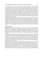
Hardware design gives an overview of the physical interaction among the devices of the
system. Hardware components of the DAS are shown in Fig. 1 below. SBC acts as an
acquisition hardware that acquires data from sensors. A signal conditioning circuit is used
for high output impedance sensor, to match the built-in ADC on the SBC board. The
developed DAS based on SBC is named Portable Embedded Sensing System (PESS). PESS is
developed with an integration of SBC, matrix keypad, LCD panel and sensors. The matrix
keypad functions as an input device and information data is displayed using LCD panel.
Fig. 2 outlines the PESS system architecture which consists of hardware and software.
Fig. 1. PESS hardware design
The PESS system has several limitations in terms of storage capacity and data view space.
Compact Flash (CF) is used as storage devices which functions as a hard disk for the SBC.
The data that can be stored on the CF is up to 4GB. Due to the limitation of CF storage
device, PESS is not suitable for applications that require large storage capacity.
4.1 Embedded acquisition hardware: TS-5500 SBC
Technologic System offers semi-custom and off-the-shelf Single Board Computers (SBC).
The product from Technologic Systems available in two different architectures which are
ARM and X86.
Portable Embedded Sensing System using 32 Bit Single Board Computer
113
Fig. 2. PESS system’s architecture
Fig. 3. TS-5500 Single Board Computer
Data Acquisition
114
For ARM SBCs, they can be identified with TS-7000 number series. There are four series for
ARM SBCs which are TS-7200 series, TS-7300 series, TS-7400 series and TS-7800 series. The
X86 SBCs is available in two series which are TS-3000 and TS-5000. The X86 SBCs have
slower CPU compared to ARM SBCs. The TS-3000 series run Intel 386 CPU with 33 MHz
and has small memory which is 8 MB. The TS-5000 series run 133 MHz AMD Elan 520 CPU
and has 32 MB of memory. The TS-5000 series is manufactured with wireless network
interface. Fig. 3 show the TS-5500 SBC main board.
TS-5500 SBC from Technologic Systems has been used by many developers in various fields
including robotic, web server application and data acquisition and control system. In 2003,
Hoopes, David, Norman and Helps presented the development of autonomous mobile robot
based on TS-5500 SBC. The other example of robotic design and development based on TS-
5500 SBC was built by Al-Beik, Meryash and Orsan.
4.2 Sensor interfacing
Two types of analog sensors are used which are temperature sensor and ion selective
electrode. LM35DZ temperature sensor from National Semiconductor is a simple analog
sensor used in this research where it’s measurement is not using a signal conditioning
circuit. Copper (Cu
2+
) ion selective electrode from Sensor Systems are used with a reference
electrode for high impedance output sensor type. Fig. 4(a) and 4(b) show the Copper ion
selective electrode and reference electrode respectively.
(a) (b)
Fig. 4. a) Copper ion-selective electrode b) Ion-selective reference electrode
The most frequently processes performed in signal conditioning are amplification, buffering,
signal conversion, linearization and filtering (Ismail, 1998). ADC normally can read analog
inputs that have low output impedance. If the input impedance of the sensor is high, the
ADC reading is unstable and not reliable. Typically the glasses electrodes such as pH probes
or gas concentration probes are of this type (Microlink, n.d.). Therefore a signal conditioning
circuit has to be integrated with a high output impedance sensor (Application notes 270,
2000). This can be done by attaching to a voltage follower as a buffer element to match the
impedance. In this research, the signal conditioning circuit built has two stages circuit. The
first stage functions as a buffer unit which will decrease the input impedance from analog
input. The second stage is a filter that removes the noise signal. The OPA2111 (OPA2111,
1993) operational amplifier is used within the signal conditioning circuit. The OPA2111 has
high internal resistance of 10
13
Ω for differential mode and 10
14
Ω for common-mode. The
signal conditioning circuit used is shown in Fig. 5.
Portable Embedded Sensing System using 32 Bit Single Board Computer
115
Fig. 5. Signal conditioning circuit
4.3 Input/Output of PESS system
The 4x4 16 button matrix keypad is used as input device for the system developed. The
keypad is manufactured by ACT Components, Inc with physical size 4.7”W x 1.7”H x 0.4”T.
A nine (9) pin input is used to connect between matrix keypad with device or processor
board using serial cable. The 24x2 alphanumeric LCD panel is use as display for this system.
The LCD is manufactured by Lumex Inc with physical size of 118mm x 36mm x 12.7mm. It
connected to processor board using 9 inputs serial cable.
(a) (b)
Fig. 6. a) 4x4 matrix keypad b) 24x2 alphanumeric LCD panel
4.4 Embedded OS: TSLinux
Technologic Systems provides two free OSes which are developed by their research team:
Linux and DOS. These OSes are developed to be used with their product only. However,
many other OSes can also be used with TS products such as uC/OS-II, eRTOS,
microCommander modular Human-Machine Interface (HMI), MicroDigital SMX modular
and QNX Embedded Real Time OS. TSLinux is chose to run on SBC in this research.
TSLinux is a PC compatible embedded Linux distribution built from open source. There is a
tailored Linux kernel for each TS SBC, along with completed driver support for the
hardware. The kernel source is also provided to end users to enable custom changes and
development.
Data Acquisition
116
Several TSLinux features as follows:
• Glibc version 2.2.5
• Kernel version 2.4.18 and 2.4.23
• Apache web server with PHP
• Telnet server and client
• FTP server and client
• BASH, ASH, minicom, vi, busybox, tinylogin
5. Software development
Two software modules developed in the PESS system which are the Analog Input
Preprocessing and Data Presentation. The Analog Input Preprocessing module involves
data acquiring from sensor, converting analog input to digital output and calculating
converted output to human readable value. A C code named sensor to cope all those
processes is developed. Data Presentation module in PESS system is handled by a program
named Interactive System. An Interactive System provides current sensor’ readings and the
information of the system such as disk (CF) usage and memory capacity status. Fig. 7 show
the interaction between both software modules which running concurrently. Sensor program
processing the analog inputs and store converted data into shared memory, meanwhile
those current data available on shared memory can be accessed via Interactive System
program.
Fig. 7. Software architecture of PESS system
5.1 Analog input preprocessing
Signals from analog sensors must be converted to digital signals before electronic device can
read them. The conversion from analog input to digital output is done using the ADC. The
digital outputs which are in binary format is then calculated into human readable value in
decimal value and presented in Volt parameter. The TS-5500 supports an eight-channel, 12-
bit ADC capable of 60000 samples per second. Each channel is independently software
programmable for a variety of analog input ranges: -10V to +10V, -5V to +5V, 0V to +10V
and 0V to +5V. The ADC control register, the Hex 196 setting is outlined by Fig. 8 below.
The IO address is read from right to left starting with 0. The settings are based on a bipolar
mode with 5V output range for all channels.
Portable Embedded Sensing System using 32 Bit Single Board Computer
117
Fig. 8. ADC control register
The processes of Analog Input Preprocessing can be divided into four stages: initialization,
bit checking, reading and storing. At the initialization stage, the permission to access ADC
IO register must be set. Three registers are involved in accessing the ADC I/O address
which are, Hex 195, Hex 196 and Hex 197. The digital output of an analog input is available
after the ADC has completely converted the input within 11µs. The End of Conversion
(EOC) status can be checked at bit 0 of register Hex 195. The conversion is completed if the
bit 0 of Hex 195 indicates ‘0’. The digital output of the converted analog input is available at
Hex 196 and Hex 197. 8 bits of them is available at Hex 196 which called as the lower 8 bits
or LSB. The other 4 bits is available at Hex 197 which called as the upper 4 bits or MSB.
Fig. 9. Analog Input Preprocessing algorithm
5.2 Data presentation
The Interactive System provides important information about the PESS system. The main
goal of the Interactive System is to display current sensors’ readings upon requested by the
user. It also provides other information of the system (PESS) such as disk usage and
memory status which viewed at the LCD panel. Another feature included in Interactive
System is a control process. This process is to enable user to restart or shutdown the PESS for
maintenance purposes. The matrix keypad functions as an input device that handles menu
selection in the Interactive System. Fig. 10 outlines the main flow chart of the Interactive
System.
Analog Input Preprocessing algorithm
Step 1 : Initialize the IO permission of ADC
Step 2 : Create and attach shared memory file descriptor
Step 3 : Set up ADC control registers
Step 4 : Check End Of Conversion (EOC) signal
4.1 If EOC signal HIGH (1)
Go to Step 4 until EOC signal LOW (0)
Step 5 : Determine input mode
: Check sign bit
Step 4 : Read all (12) digital output (LSB and MSB)
Step 5 : If input mode negative
5.1 Perform two’s compliment
Step 6: Convert binary value (digital output) to decimal value
Step 7: Store converted reading into shared memory
Step 8: End
Data Acquisition
118
Start
Load LCD driver
Load keypad driver
Input == 1 ?
Yes
No
Display “System
Starting”
Display menu selection
Input == 2 ?
Yes
No
Input == 3 ?
Yes
No
System info Control system Sensor reading
EndWhile true
Yes
No
Fig. 10. Interactive System flowchart
Three options are provided: to check current sensors’ readings, to check systems’
information or to control the system. Three subroutines are created to handle those
processes which are system info, control system and sensor reading as outlined by Fig. 10 above.
Actually the processes of these three subroutines are carried out by combining the binary C
code and shell scripts. Shell scripts retrieve current sensors’ readings which are processed
by the sensor program, and manipulate Linux commands to retrieve system information and
control the system. The binary C code grabs the data given by the shell script codes and
displays them.
6. PESS implementation
Standard method to gain the result of environment parameters such as water and air quality
is using laboratory experiment. The laboratory experiment is not suitable for long period
testing work such as in monitoring process. The alternatives method can resolve that
Portable Embedded Sensing System using 32 Bit Single Board Computer
119
limitation. The US Environment Protection Agency (EPA) define alternatives method as any
method but has been demonstrated in specific cases to produce results adequate for
compliance monitoring (Quevauviller, 2006).
The alternatives method leads to real-time data sampling which can produce instant output
result for in situ deployment. It also provides easier usage with advance electronic devices in
a compact size but can perform multitasks excellently. The handheld instrument usage is
one of the alternatives methods such as using Data Acquisition (DAQ) device. The DAQ
device such as SBC offers variety of peripherals to make it function as a standalone system.
Meanwhile the ion specific electrodes is also been used in many application with handheld
instrument. For example, non-invasive chemical sensor arrays provide a suitable technique
for in situ monitoring (Bourgeois, 2003). Many researches use specific ion selective electrode
or sensor array for detection of target environmental substance or gases (Carotta, 2000;
Becker, 2000; Wilson, 2001; Lee, 2001).
The measurement of the LM35DZ temperature sensor is done without connecting the signal
conditioning circuit. The LM35DZ sensors are only given a power supply and grounding.
The sensor’ outputs are connected directly to ADC port of SBC during measurement. Fig. 11
shows the experimental setup to acquire ion selective electrode’s reading. Three parts
involve here are: (1) SBC, (2) Sensors (electrodes) and (3) Signal conditioning circuit. While
the red arrows marks from point A and B are the input and output from signal conditioning
circuit respectively. Sensor reading’ results are presented in next section.
Fig. 11. Experimental setup of ion-selective electrodes
The programs called sensor and Interactive System are developed to handle all processes
involved in Analog Input Preprocessing and Data Presentation modules respectively. Both
modules are running separately but have a relationship in terms of data sharing. Fig. 12
outlines the state diagram for PESS system and the running processes listing. The current
running process on PESS system including sensor and Interactive System as underlined in
figure below. Analog Input Preprocessing module acquires data from sensors and storing
converted data in a shared memory at PESS. These processes are repeated again with new
inputs after certain time interval. While the Interactive System retrieve those converted data
from shared memory and view it at LCD panel.
Data Acquisition
120
Fig. 12. PESS state diagram and running process listing
Four processes (programs) are set up to automatically start during the boot up program. The
processes are: inserting the matrix keypad driver module; running sensor process; running
the scripts (info.sh, reading.sh and control.sh) of Interactive System; and running the Interactive
System program itself. These processes are underlined in Fig. 13. This procedure can be done
by configuring how process will start up at /etc/init.d directory.
Fig. 13. Start processes automatically during system boot up
Portable Embedded Sensing System using 32 Bit Single Board Computer
121
The integration between the SBC, the matrix keypad and the alphanumeric LCD display is
to create an Interactive System for a standalone system. Fig. 14(a) shows the components that
are connected to allocated ports. A serial ribbon cable is used to connect the matrix keypad
and LCD panel to pin ports on SBC. Fig. 14(b) and Fig. 14(c) show the menu selection of
Interactive System and current sensor’ readings respectively.
(b)
(a) (c)
Fig. 14. a) Hardware used in Interactive System b) Interactive System menu selection c)
Example of current sensor’ readings
7. Result and discussion
Bit error is the value of an encoded bit that has been changed due to a transmission problem
such as noise in the line and which is then interpreted incorrectly. Commonly notated as bit
error ratio (BER), the ratio of the number of failed bits to the total number of bits calculated.
The number of bits in the ADC determines the resolution of the data acquisition system.
The resolution of an ADC is defined as follow (Principle of Data Acquisition and Conversion,
1994);
FSR
n
V
Resolution One LSB
2
==
(1)
Where V
FSR
is a full scale input voltage range and n is the number of bits.
The ADC is set up to read all eight analog channels using bipolar mode within 5V range.
Therefore the total output range is 10V which are from -5V to +5V. The step resolution of
digital output is calculated as below;
n = 12
V
FSR
= 10V ( -5 V to +5 V)
12
10 V
Resolution 2.44
2
mV==
Analog input reading verification is the important part in PESS development as it will
ensure that the sensor’ readings is correct and reliable. Verification testing of analog input
reading is carried out by checking the output of each ADC channels. DC power supply is
used as input to ADC and tapped manually to every channel. In a single reading, only one
channel is given 1.0 V input while the rest is given 0 V using ground signal of SBC. The first
Data Acquisition
122
1.0 V input is given to channel 7, then to channel 6 until the last channel, channel 0. Fig. 15
shows the input from DC power supply while Fig. 16 show the result of analog input
reading verification testing. From Fig. 15, the input from DC power supply is 1.002V as
displayed by digital multimeter.
Fig. 15. Input from DC power supply
Fig. 16. Analog input reading verification output
Every channel is given 0 V input for first reading as shown in first line in Fig. 16. The error
recorded in first line reading is 2.44 mV which is given by channel 1 which equals to 1 step
resolution. Then 1.0 V input is given to channel 7 as shown by the second reading and for
other channels the input given is 0V. The reading is presented in 2 floating point. From Fig.
16, the readings recorded are 1001.47 mV and 999.02 mV for channels that was given 1.0 V
input. The reading variants are 0.53 mV and 2.98 mV respectively. From the results above,
the analog input reading has small error which are 1 and 2 step resolutions so that the
readings is considered reliable.
The readings of temperature sensor at room temperature is around 1110 mV and 1120 mV as
shown by line 1 until line 5 in Fig. 17 below. Heat was forced to the temperature sensor
using a lighter (fire) for a few seconds. The readings are increased at the moment the heating
process as shown by line 6 until line 10 in Fig. 17.
A measurement of ion-selective electrodes is carried out to observe their output reading
reliability. The reading of ion-selective electrodes are considered reliable if their readings are
stable and do not fluctuate. The Copper electrode is tested with Copper standard solution
which has been produced by mixing sterile water and Copper liquid. In this research, five
different standard solution densities are used: 10 ppm, 20 ppm, 30 ppm, 40 ppm and 50
ppm. Firstly, the Copper sensor is tested using 10 ppm standard solution. The Copper ion-
selective electrode together with the reference electrode are immersed in 10 ppm Copper
Portable Embedded Sensing System using 32 Bit Single Board Computer
123
standard solution. Measurement is started five minutes after those electrodes immersed. The
measurement is repeated for 20 ppm of Copper standard solution. These steps are repeated
until the standard solution reaches 50 ppm. Fig. 18 shows the reading of Copper ion-
selective electrode. From the graphs, the readings are decrease with higher standard
solution density for each case.
Fig. 17. LM35DZ temperature sensor readings
Fig. 18. Copper sensor’s reading versus standard solution density
8. Conclusion
Data Acquisition System (DAS) is one of common system currently applied in industrial
application such as automation control, alert system and monitoring system. The
advancement of electronic technology has led to tremendous applications using embedded
systems. Embedded based application has led to portable and small form factor system with
medium or high speed processor. In this research, a DAS has been developed using a 32bit
Single Board Computer (SBC). The developed DAS is an integration of SBC, matrix keypad
and LCD display and named as Portable Embedded Sensing System (PESS). PESS can be
used as a data logger for a short term data collection which can provide immediate results
for portable works either for indoor or outdoor experiment.
Data Acquisition
124
Two software modules developed in PESS systems which are Analog Input Preprocessing
and Data Presentation. The processes involved in Analog Input Preprocessing are acquiring
analog sensor’s input, converting analog signal to digital signal and calculating digital
output to human readable values. These processes are done by a program named sensor. An
Interactive System handles input given by user via matrix keypad and output to the LCD
display for Data Presentation modules.
PESS has limited data storage capacity since it used a Compact Flash (CF) to store
temporary data. This system also has limitation in term of visualization where data are
viewed via LCD panel. These limitation can be enhanced by extending the PESS system into
a network based DAS. PESS system can be used as Sensor Node (SN) that collecting data
from fields and sending the collected data to the server that able in providing larger storage
capacity. The user interface can be developed to provide interactive data presentation which
can be access remotely via internet. The network based DAS is normally applied in
monitoring system especially for long period and scheduled activities.
9. References
Al-Beik, H., Meryash, N. & Orsan, I. A. (2005). Detect, Verify, Locate, Build (DVLB) Rover.
Project Report, Worcester Polytechnic Institute.
Alderighi, M., Anzalone, O., Bartolucci, M., Cardella, G., Cavallaro, S., De Filippo, E., et al.
(2002). CHIMERA data acquisition and computational system using DSP-based
VME modules. IEEE Transactions on Nuclear Science, 49(2), 432-436.
Application Notes 270. (2000). Analog-Signal Data Acquisition in Industrial Systems. Retrieved
April 14, 2006 from
Baxter, M. (2001). Embedded Linux SBCs. Linux Journal. Retrieved March 23, 2006 from
/>4726/4726t1.html
Becker, T., Mühlberger, S., Braunmühl C. Bosch-v., Müller, G., Ziemann, T & Hechtenberg,
K. V. (2000). Air pollution monitoring using tin-oxide-based microreactor system,
Sensors and Actuators B: Chemical, 69(1-2), 108-119
Bourgeois, W., Romain, A-C, Nicolas, J. & Stuetz, R. M. (2003). The use of sensor array for
environmental monitoring: interests and limitations. Journal of Environmental
Monitoring, 5, 852-860.
Burckle, R. A., (n.d.). The Evolution of Single Board Computers. Retrieved Jun 30, 2006 from
Carotta, M. C., Martinelli, G., Crema, L., Gallana, M., Merli, M., Ghiotti, G et al. (2000). Array
of thick film sensors for atmospheric pollutant monitoring, Sensors and Actuators B:
Chemical, 68(1-3), 1-8.
Eyre, J. & Bier, J. (2000). The evolution of DSP processors. IEEE Signal Processing Magazine,
17(2), 43-51.
Hansen, S., Jordan, T., Kiper, T., Claes, D., Snow, G., Berns, H., Burnett, T. H., Gran, R. &
Wilkes, R. J. (2004). Low-cost data acquisition card for school-network cosmic ray
detectors. IEEE Transaction on Nuclear Science, 51(3), 926-930.
Hoopes, D., Davis, T., Norman, K. & Helps, R. (2003). An Autonomous Mobile Robot
Development for Teaching a Graduate Level Mechatronics Course. Proceedings of
Portable Embedded Sensing System using 32 Bit Single Board Computer
125
33
rd
ASEE/IEEE Frontiers in Education Conference, F4E-17-F4E22. Retrieved March 23,
2006
Ismail, Y. (1998). Data Acquisition System with Embedded Digital Signal Processor for
Instrumentation/Control Applications (Design and Implementation). Degree Thesis,
Universiti Islam Malaysia.
James, K. (2000). PC Interfacing and Data Acquisition Techniques for Measurement,
Instrumentation and Control. Oxford: Newnes.
Laymon, C. M., Miyaoka, R. S., Park, B. K. & Lewellen, T. K. (2003). Simplified FPGA-based
data acquisition system for PET. IEEE Transactions on Nuclear Science, 50(5), 1483-
1486.
Lee, D-D. & Lee, D-S. (2001). Environmental gas sensors, IEEE Sensors Journal, 1(3), 214-224.
LinuxDevices (n.d.). A Linux-oriented Intro to Embeddable Single Board Computers. Retrieved
March 23, 2006 from
Martin, S. (1990). PC-based Data Acquisition in an Industrial Environment. IEE Colloquium
on PC-Based Instrumentation, 2/1 – 2/3.
Microlink. (n.d.) Technical Notes: Data Acquisition Techniques. Retrieved May 13, 2006 from
Misal, C. S. & Conrad, J.M. (2007). Designing a pH data acquisition and logging device using
an inexpensive microcontroller. IEEE Proceedings SoutheastCon, 217-220.
Ng, K. Y. (1994). General Purpose Data Acquisition and Process Control System. Degree Thesis,
Universiti Malaya.
Omata, K., Fujita, Y., Yoshikawa, N., Sekiguchi, M. & Shida, Y. (1992). A Data Acquisition
System based on a Personal Computer. IEEE Transaction on Nuclear Science, 39(2),
143-147.
OPA2111 (1993). Dual Low noise precision difet operational amplifier. Retrieved April 14, 2006
from
Perera, A., Gutierrez-Osuna, R., & Marco, S. (2001). IPNOSE: A Portable Electronic Nose
Based on Embedded Technology for Intensive Computation and Time Dependent
Signal Processing. Proceeding of the 8
th
Intl. Symp. On Olfaction an Electronic Nose, 1-6.
Peters, B., Wardrop, A., Lahti, D., Herzog, H., O'Connor, T., & DeCoursey, R. (2007). Flight
SEU Performance of the Single Board Computer (SBC) Utilizing Hardware Voted
Commercial PowerPC Processors On-board the CALIPSO Satellite. IEEE Radiation
Effects Data Workshop 2007, 0, 16-25.
Quevauviller, P, Thomas, O. & Beken, A. V-D. (2006). Wastewater Quality Monitoring and
Treatment. West Sussex, England: Wiley.
Rangnekar, S., Nema, R. K. & Raman, P. (1995). PC based data acquisition and monitoring
system for synchronous machines. IEEE/IAS International Conference on Industrial
Automation and Control, 195-197.
Riley, T. C., Endreny, T. A. & Halfman, J. D. (2006). Monitoring soil moisture and water
table height with a low-cost data logger. Computers & Geosciences, 32(1), 135-140.
Rongen, H. (n.d.). Introduction to PC-Based Data Acquisition Systems. Retrieved October 23,
2006 from
Wilson, D. M., Hoyt, S., Janata, J., Booksh, K. & Obando, L. (2001). Chemical sensor for
portable, handheld field instruments, IEEE Sensors Journal, 1(4), 256-274.
Data Acquisition
126
Zabolotny, W. M., Roszkowski, P., Kierzkowski, K., Pozniak, K., Romaniuk, R. & Simrock, S.
(2003). Distributed Embedded PC Based Control and Data Acquisition System for TESLA
Cavity Controller and Simulator. Retrieved March 16, 2007 from
/>34.pdf
7
Microcontroller-based Data Acquisition
Device for Process Control
and Monitoring Applications
Vladimír Vašek, Petr Dostálek and Jan Dolinay
Tomas Bata University in Zlín
Czech Republic
1. Introduction
Process measurement is one of the most important tasks in the whole control system. It is
determined by the fact that control accuracy is fully dependent on how preciously
measuring chain works. Present-day there is available number of devices performing data
acquisition tasks – standard cards for PCI or ISA bus which are suitable for standard
personal computers and its industrial versions and modules for industrial automation
usually equipped with RS485, CAN and other interfaces. Independent category is formed by
smart sensors incorporating sensor, converter to unified signal and data acquisition device
in one embedded system with very compact dimensions and low power consumption. They
have number of advantageous features such as automatic diagnostic and calibration, high
accuracy and immunity against electromagnetic interference due to short signal paths. On
the other hand lower operating temperature range reduces their usage to laboratory
applications, automotive and aircraft industry where compact dimensions and low weight
are crucial. Quite often occurred situations when it is necessary to measure data in terrain
where it is not possible to use standard computer equipped with DAQ card. In these cases
laptop computer equipped with portable data acquisition device may be very advantageous.
On the market are available devices equipped with USB 2.0 connectivity which can fully
functionally substitute PCI cards. But they are not able to work without connected computer
which must continually control all DAQ operations. Therefore it is not possible to use them
in applications where is required long-term monitoring and archiving process quantities in
distant areas without access to mains power.
This contribution proposes design of multi-channel portable data acquisition device based
on low cost general-purpose 8-bit microcontroller Freescale 68HC908GP32, which was
developed in our department mainly for control and monitoring educational laboratory
models. First part deals with hardware design of the DAQ device with focus on description
of operation of individual functional blocks. After that follows description of internal
software (firmware) based on real-time operating system RTMON for HC08, which was
developed on our department especially for microcontroller-based embedded systems with
CPU08 main processor core. Next chapters discuss DAQ device software support in form of
program libraries for MS Visual C++, Control Web and Matlab/Simulink development
environments, which can significantly improve development time of new process control or
Data Acquisition
128
monitoring applications. And finally last part deals with verification of the developed DAQ
device with control of selected laboratory model.
2. Data acquisition device hardware design
2.1 Hardware overview
Hardware design of the DAQ device is fully adopted to support 16 analog inputs with 12-bit
resolution, 8 digital inputs and outputs and one analog output with 12-bit resolution with
stress on low power consumption enabling long operation when battery supply is used. The
core of the DAQ device is 8-bit general purpose Motorola microcontroller 68HC908GP32
with Von-Neumann architecture which is fully up-ward compatible with the 68HC05
family. On the chip are integrated timer interface with input capture and output compare
functions, 8-channel analog-to-digital converter with 8-bit resolution, up to 33 general-
purpose I/O pins, clock generator module with PLL, serial communication interface and
serial peripheral interface. M68HC908GP32 has implemented several protective and security
functions such as low-voltage inhibit which monitors power supply voltage, computer
operates properly (COP) counter and FLASH memory protection mechanism preventing
unauthorized reading of the user’s program. Internal RAM memory has capacity of 512B
and FLASH memory 32 KB. Internal clock frequency can be 8 MHz at 5 V operating voltage
or 4 MHz at 3 V operating voltage. Microcontroller also supports wait and stop low-power
modes (Freescale, 2008)
Central processor unit CPU08 which is the main part of M68HC908GP32 microcontroller is
fully object code compatible with M68HC05. This feature allows easy code migration to new
architecture providing high speed, low power and better processing capabilities.
Central processor unit features can be summarized in the following points:
- 8 MHz bus speed at 5 V, 4 MHz bus speed at 3 V
- 16-bit stack pointer with new stack manipulation instructions
- 16-bit index register with index register instructions
- 78 new instructions
- Memory to memory moves without using the accumulator
- 16 addressing modes including stack relative
- 64 Kbytes program/data memory space
- Fully static low-voltage/low-power design (Freescale, 2006)
Analog-to-digital conversion is performed by the A/D converter Linear Technology
LTC1298. It is micro power, 2-channel, 12-bit switched-capacitor successive approximation
sampling A/D converter which can operate on 5 V to 9 V power supplies. Communication
with microcontrollers is handled by 3-wire synchronous serial interface. It typically draws
only 250μA of supply current during conversion and only 1nA in power down mode in
which enters after each conversion (Linear Technology, 1994).
Digital-to-analog circuit utilizes 12-bit D/A converter Burr-Brown DAC7611 with internal
2.435V reference and high speed rail-to-rail amplifier. It requires a single 5 V supply. Power
consumption is only 2.5 mW at 5 V. Build-in synchronous serial interface is compatible with
variety of digital signal processors and microcontrollers (Burr-Brown, 1998).
2.2 Circuits design
Electronic circuits of the data acquisition device can be divided into the seven main
functional blocks as depicted in the Fig.1: analog-to-digital converter with analog
Microcontroller-based Data Acquisition Device for Process Control and Monitoring Applications
129
multiplexer circuits, microcontroller circuits, digital-to-analog converter and amplifier
circuits, digital I/O driver circuits, serial communication interface RS232 and finally power
supply circuits.
Fig. 1. Block diagram of the DAQ device
MCU circuits (Fig.2) incorporate all electronics circuits needed for correct function of the
microcontroller M68HC908. They consists of Pierce crystal oscillator with output frequency
of 32.768 kHz connected to OSC1 and OSC2 pins of the MCU and filter network (parts R3,
C3, C4) needed by internal phase-locked loop circuit (PLL) allowing programmable
selection of output frequency. Reset (RST) and interrupt request (IRQ) pins are permanently
connected through pull-up resistors R4 and R5 to high level, because their function is not in
data acquisition device used. Reset of the MCU is automatically generated after power on by
internal circuits of the microcontroller. Output frequency of the Pierce oscillator is by
internal PLL circuit increased to 32 MHz resulting in internal bus clock frequency of 8 MHz
which is used as reference frequency of the CPU and most internal peripherals. Ports PTA
and PTB are completely dedicated for digital input and output functions except pin
PTB0/AD0 which is used in its alternative function as input of analog-to-digital converter
for monitoring of accumulator battery voltage. Low voltage condition occurs when supply
voltage drops below 6.5 V. So voltage of the one NiMH accumulator in the battery drops to
1.08 V indicating that approximately 80 - 90 % of its capacity is discharged. Correct DAQ
device operation is guaranteed at minimum voltage of 5.5 V. Pin PTD3 is connected to the
LED diode indicating status of the device. PTD0 to PTD2 pins provides binary selection of
active input analog channel, PTC0 to PTC4 pins perform synchronous serial communication
with A/D and D/A converters.
Digital input / output driver circuit (Fig.3) has two important functions. Firstly, it protects
microcontroller inputs from electrostatic discharge which may occur during handling and
connecting DAQ device to the measured object and secondly, it boosts output current from
microcontroller pins and protects them against overload or short-circuits. It uses two non
inverting 3-state high-speed octal bus buffers 74HC244 with 35mA maximum current
output capability per pin.
Analog multiplexer + A/D
MCU
circuits
I/O
driver
D/A +
amplifier
Serial
communications
interface
Power supply circuits
.
.
.
.
.
.
16x analog
inputs
8x di
g
ital
8x di
g
ital in
p
uts
1x analog output
RS232 RX
RS232 TX
9V DC input
Data Acquisition
130
Fig. 2. Microcontroller circuits schematics.
Fig. 3. Digital input/output buffer schematics.
Analog multiplexer, A/D and D/A converter circuits schematics is depicted in the Fig.4.
Measured analog voltage signals 0 - 10 V first enters the input dividers performing signal
conditioning to voltage range of 0 - 5 V to meet specifications of analog-to-digital converter.
Microcontroller-based Data Acquisition Device for Process Control and Monitoring Applications
131
Fig. 4. Analog multiplexer, A/D and D/A converter circuits schematics.
After that they are switched by two 8-channel high-speed analog multiplexers 74HC4051 to
the two input analog channels CH0 and CH1 of 12-bit A/D converter LTC1298. Input
channel pair selection is realized by MCU pins PTD0, PTD1 and PTD2. Microcontroller
communicates with A/D converter using pins PTC1 (data clock), PTC2 (serial data in/out)
and PTC4 (chip select). One conversion is done after 16 clock signal periods resulting in
maximum of 12.5 kHz sampling rate at clock frequency of 200 kHz.
Analog output circuits are based on digital-to-analog converter DAC7611 with 12-bit
resolution. It is controlled by MCU pins PTC0 (chip select), PTC1 (data clock), PTC2 (serial
data in) and PTC3 (load/strobe). One D/A conversion takes place after 12 clock periods,
output settling time is 7μs to 1 LSB. At the converter output is connected operational
amplifier MC1458 in non-inverting configuration amplifying output D/A voltage to the
standard range of 0 – 10 V. Exact output range can be adjusted by variable resistor R19.
Data acquisition device contains three independent power supplies. Digital parts (MCU
circuits, input/output driver, serial communications interface and D/A converter) are
supplied by circuit depicted in the Fig.5. It uses low-drop 5V/1A regulator LM2940 in
Data Acquisition
132
manufacturer’s recommended wiring enabling correct operation with input voltage down to
5.5 V. Input of the supply is protected against overloading or polarity reversing by fast
acting fuse. Analog-to-digital converter is supplied from high-precision voltage reference
LM336-Z5.0 which is connected to adjustable current source LM334. Output voltage can be
adjusted to the exact 5 V value by variable resistor R18 (Fig.6). Analog output amplifier is
supplied by DC-DC converter ICL7662 providing positive and negative voltages for analog
output operational amplifier from single supply.
Fig. 5. Power supply for digital circuits schematic
Fig. 6. Power supply for A/D converter schematics
Serial communications interface utilizes standard TTL to RS232 and RS232 to TTL converter
MAX232 in manufacturer’s reference wiring (Fig. 7). It is connected to microcontroller via
pins PTE0/TxD and PTE1/RxD to serial communications module.
Data acquisition device is realized on two printed circuit boards (PCB), which are connected
together using single row pin headers. First PCB (Fig.8 – left picture) contains mainly digital
circuits – microcontroller, input / output drivers and serial communications interface. It also
carries main +5V power supply equipped with low-drop voltage regulator. While second
PCB (Fig.8 – right picture) incorporates all analog signal processing circuits – analog-to-
digital and digital-to-analog converter, output amplifier, analog multiplexers, DC-DC
converter and finally reference voltage source for A/D converter. Device features are
summarized in Table 1.
Microcontroller-based Data Acquisition Device for Process Control and Monitoring Applications
133
Fig. 7. Serial communication interface schematics
Fig. 8. Finalized DAQ device printed circuit boards
Digital inputs 8 channels, TTL compatible
Digital outputs 8 channels, TTL compatible
Analog inputs 16 channels, 12 bits resolution, input range 0 – 10 V
Analog outputs 1 channel, 12 bits resolution, output range 0 – 10 V
Supply voltage 6.5 to 9V DC
Communication RS232 interface, 57600 Bd, 8-bit data, 1 start bit, 1 stop bit
Table 1. Technical parameters of the DAQ device
Data Acquisition
134
Fig. 9. Photograph of the prototype DAQ unit
3. DAQ device firmware design
DAQ device internal software is based on real-time operating system RTMON for HC08,
which was developed on our department especially for microcontroller-based embedded
systems with CPU08 main processor core. So software is formed of RTMON core and
individual processes which perform all necessary tasks. Each process activity is controlled
by operating system core on the basis of process priority and other information stored in the
task descriptor. Structure of the DAQ device firmware is depicted in the Fig. 10. There are 4
main processes and 1 interrupt handling routine. RTMON core and program processes
functions are described in chapters 4.1 and 4.2.
Fig. 10. Internal software structure
RTMON
Process 2
Command processing
Process 1
S
y
stem initialization
Process 3
PWM modulation
Process 4
Communication
SCI
Read received
character from SCI
and write it to buffer.
Return
Microcontroller-based Data Acquisition Device for Process Control and Monitoring Applications
135
3.1 Real-time operating system RTMON
RTMON is preemptive multitasking operating system which is simplified to great extend to
allow easy use for programmers. It is written in C language with the exception of small
platform-specific code written in assembler. The scheduler assigns time slices to processes
based on their priority. The priority is integer in the range 1 to 254. Priority 0 is the highest
and is reserved for the RTMON initialization process and priority 255 is the lowest and is
reserved for the idle process (called dummy in RTMON).
RTMON allows execution of two different types of processes (tasks): normal processes
which execute only once (such process typically contains infinite loop) and periodical
process which is started automatically by RTMON with given period. These periodical
processes are useful for many applications, for example, in discrete controllers which need
to periodically sample the input signal and update the outputs.
For the sake of simplicity of both the implementation and usage, several restrictions are
applied. First, the RAM memory for processes and their stacks is statically allocated for the
maximal number of processes as defined in configuration file. In the user program, it is not
possible to use this memory even if there are fewer processes defined. In case more RAM is
needed for the user program, the maximum number of tasks and/or stack-pool size can be
changed in configuration file and the RTMON library must be rebuild.
The priority of each task must be unique, so that in each moment one task (the one with
highest priority) can be selected and executed on the CPU. The scheduler does not support
cyclical switching of several processes with the same priority on the CPU in round-robin
fashion; it simply chooses the task with highest priority from the list of tasks which are
ready to run. Processes can be created on the fly, but it is not possible to free and reuse
memory of a process. No more than the maximal number of processes can be created, even
if some processes were previously deleted.
These restrictions, however, do not present any big problem for most applications and allow
for small kernel code size and ease of use.
There are only two objects (data structures) which RTMON contains: process (task) and
queue. The queues are buffers for transferring data between processes. It would more
properly be called mailboxes in our implementation as each queue can contain only 1
message. Several queues can be created, each containing a message (data buffer) of certain
size. The size can be specified when creating the queue and is limited by the total size of
RAM reserved for all buffers of all the queues (queue pool size). Processes can read and
write data to the queue and wait for the queue to become empty or to become full. This
allows for use of the queue also as a synchronization object (semaphore).
The RTMON uses timer interrupt which occurs at certain period (e.g. 10 ms) to periodically
execute the scheduler, which decides which process will run in the next time slice. The timer
interrupt routine is implemented in assembly language. It first stores CPU registers onto the
stack and then calls RTMON kernel, which is a C function. The kernel then finds the process
with highest priority which is in ready-to-run state and switches the context, so that the
code of this process is executed after return from the interrupt service routine. If no process
is ready to run, then a special dummy process is executed. This dummy process is contained
within RTMON code and does nothing.
The following basic operations can be performed with a process in RTMON. Each operation
corresponds to a function in the RTMON library which user program can call:
- create process
- start process