Solar energy 2012 Part 5 pdf
Bạn đang xem bản rút gọn của tài liệu. Xem và tải ngay bản đầy đủ của tài liệu tại đây (1.1 MB, 30 trang )
Efficiency of Thin-Film CdS/CdTe Solar Cells
113
λ
λ
λη
Δ
Φ
=
∑
i
hv
qJ
i
i
intsc
)(
)(
, (12)
where ∆λ
i
is the wavelength range between the neighboring values of λ
i
(the photon energy
h
ν
i
) in the table and the summation is over the spectral range
λ
<
λ
g
= hc/E
g
.
3.1 The drift component of the short-circuit current
Let us first consider the drift component of the short-circuit current density J
drift
using Eq. (12).
Fig. 5 shows the calculation results for J
drift
depending on the space-charge region width W.
In the calculations, it was accepted φ
o
– qV = 1 eV, S = 10
7
cm/s (the maximum possible
velocity of surface recombination) and S = 0. The Eq. (9) was used for η
int
(
λ
).
Important practical conclusions can be made from the results presented in the figure.
If S = 0, the short-circuit current gradually increases with widening of W and approaches a
maximum value of J
drift
= 28.7 mA/cm
2
at W > 10 μm (the value J
drift
= 28.7 mA/cm
2
is
obtained from equation (12) at
η
drift
= 1).
10
18
10
16
10
14
10
12
S = 10
7
cm/s
S = 0
N
a
–
N
d
(c
m
–
3
)
I
drift
(mA/cm
2
)
28.7 mA/cm
2
0.01 0.1 1.0 10 100
0
10
20
30
W (µm)
Fig. 5. Drift component of the short-circuit current density J
drift
of a CdTe-based solar cell as
a function of the space-charge region width W (the uncompensated acceptor concentration
N
a
– N
d
) calculated for the surface recombination velocities S = 10
7
cm/s and S = 0.
Such result should be expected because the absorption coefficient
α
in CdTe steeply
increases in a narrow range h
ν
≈ E
g
and becomes higher than 10
4
cm
–1
at h
ν
> E
g
. As a result,
the penetration depth of photons
α
–1
is less than ∼ 1 μm throughout the entire spectral range
and in the absence of surface recombination, all photogenerated electron-hole pairs are
separated by the electric field acting in the space-charge region.
Surface recombination decreases the short-circuit current only in the case if the electric field
in the space-charge region is not strong enough. The electric field decreases as the space-
charge region widens, i.e. when the uncompensated acceptor concentration N
a
– N
d
decreases. One can see from Fig. 5 that the influence of surface recombination at
N
a
– N
d
= 10
14
-10
15
cm
–3
is quite significant. However, as N
a
– N
d
increases and consequently
the electric field strength becomes stronger, the influence of surface recombination becomes
Solar Energy
114
weaker, and at N
a
– N
d
≥
10
16
cm
–3
the effect is virtually eliminated. However in this case, the
short-circuit current density decreases with increasing N
a
– N
d
because a significant portion
of radiation is absorbed outside the space-charge region.
It should be noted that the fabrication of the CdTe/CdS heterostructure is typically
completed by a post-deposition heat treatment. The annealing enables grain growth,
reduces defect density in the films, and promotes the interdiffusion between the
CdTe and CdS layers. As a result, the CdS-CdTe interface becomes alloyed into the
CdTe
x
S
1-x
-CdS
y
Te
1-y
interface, and the surface recombination velocity is probably reduced to
some extent (Compaan et al, 1999).
3.2 The diffusion component of the short-circuit current
In order to provide the losses caused by recombination at the CdS-CdTe interface and in the
space-charge region at a minimum we will accept in this section N
a
– N
d
≥ 10
17
cm
–3
. On the
other hand, to make the diffusion component of the short-circuit current J
dif
as large as
possible, we will set
τ
n
= 3×10
–6
s, i.e. the maximum possible value of the electron lifetime in
CdTe. Fig. 6(a) shows the calculation results of J
dif
(using Eqs. (10) and (12)) versus the CdTe
layer thickness d for the recombination velocity at the back surface S = 10
7
cm/s and S = 0
(the thickness of the neutral part of the film is d – W).
One can see from Fig. 6(a) that for a thin CdTe layer (few microns) the diffusion component
of the short-circuit current is rather small. In the case S
b
= 0, the total charge collection in the
neutral part (it corresponds to J
dif
= 17.8 mA/cm
2
at
η
dif
= 1) is observed at d = 15-20 μm.
To reach the total charge collection in the case S
b
= 10
7
cm/s, the CdTe thickness should be
50 μm or larger. Bearing in mind that the thickness of a CdTe layer is typically between
2 and 10 µm, for d = 10, 5 and 2 µm the losses of the diffusion component of the short-circuit
current are 5, 9 and 19%, respectively. The CdTe layer thickness can be reduced by
shortening the electron lifetime
τ
n
and hence the electron diffusion length L
n
= (
τ
n
D
n
)
1/2
.
However one does not forget that it leads to a significant decrease in the value of the
diffusion current itself. This is illustrated in Fig. 6(b), where the curve J
dif
(
τ
n
) is plotted for a
thick CdTe layer (50 μm) taking into account the surface recombination velocity
S
b
= 10
7
cm/s. As it can be seen, shortening of the electron lifetime below 10
–7
-10
–6
s results
in a significant lowering of the diffusion component of the short-circuit current density.
Thus, when the space-charge region width is narrow, so that recombination losses at the
CdS-CdTe interface can be neglected (as seen from Fig. 5, at N
a
– N
d
> 10
16
-10
17
cm
–3
), the
conditions for generation of the high diffusion component of the short-circuit current are
d > 25-30 μm and
τ
n
> 10
–7
-10
–6
s.
In connection with the foregoing the question arises why for total charge collection the
thickness of the CdTe absorber layer d should amount to several tens of micrometers. The
value d is commonly considered to be in excess of the effective penetration depth of the
radiation into the CdTe absorber layer in the intrinsic absorption region of the
semiconductor. As mentioned above, as soon as the photon energy exceeds the band gap of
CdTe, the absorption coefficient
α
becomes higher than 10
4
cm
–1
, i.e. the effective
penetration depth of radiation
α
–1
becomes less than 10
–4
cm = 1 μm. With this reasoning,
the absorber layer thickness is usually chosen at a few microns. However, all that one does
not take into the account, is that the carriers arisen outside the space-charge region, diffuse
into the neutral part of the CdTe layer penetrating deeper into the material. Carriers reached
the back surface of the layer, recombine and do not contribute to the photocurrent. Losses
Efficiency of Thin-Film CdS/CdTe Solar Cells
115
0 10 20 30 40 50
10
15
20
S
b
= 10
7
cm/s
S
b
= 0
d
(
μ
m
)
I
dif
(mA/cm
2
)
17.8 mA/cm
2
(a)
5
10
15
20
10
–
9
10
–
8
10
–
7
10
–
6
17.8 mA/cm
2
10
–
10
10
–
5
τ
n
(s)
J
dif
(mA/cm
2
)
(b)
Fig. 6. Diffusion component of the short-circuit current density J
dif
as a function of the CdTe
layer thickness d calculated at the uncompensated acceptor concentration N
a
– N
d
= 10
17
cm
–3
,
the electron lifetime
τ
n
= 3×10
–6
s and surface recombination velocity S
b
= 10
7
cm/s and S
b
= 0
(a) and the dependence of the diffusion current density J
dif
on the electron lifetime for the CdTe
layer thickness d = 50 μm and recombination velocity at the back surface S
b
= 10
7
cm/s (b).
caused by the insufficient thickness of the CdTe layer should be considered taking into
account this process.
Consider first the spatial distribution of excess electrons in the neutral region governed by
the continuity equation with two boundary conditions. At the depletion layer edge, the
excess electron density Δn can be assumed equal zero (due to electric field in the depletion
region), i.e.
Δn = 0 at x = W. (13)
At the back surface of the CdTe layer we have surface recombination with a velocity S
b
:
bn
dn
Sn D
dx
Δ
Δ=− at x = d, (14)
where
d is the thickness of the CdTe layer.
Using these boundary conditions, the exact solution of the continuity equation is (Sze, 1981)
:
n
o
22
nn
bn
n
nn n
n
bn
nn n
() () exp[ ]cosh exp[ ( )]
1
cosh exp[ ( )] sinh exp[ ( )]
sinh
sinh cosh
xW
nT N W xW
LL
SL dW dW
dW L dW
DL L
xW
L
SL xW dW
DL L
ατ
λλ α α
α
ααα
⎧
⎛⎞
−
⎪
Δ= − − − − −
⎨
⎜⎟
−
⎪
⎝⎠
⎩
⎡⎤
⎛⎞ ⎛⎞
−−
−−− + + −−
⎢⎥
⎜⎟ ⎜⎟
⎫
⎛⎞
−
⎪
⎝⎠ ⎝⎠
⎣⎦
−×
⎬
⎜⎟
⎛⎞⎛⎞
−−
⎪
⎝⎠
⎭
+
⎜⎟⎜⎟
⎝⎠⎝⎠
(15)
where
T(
λ
) is the optical transmittance of the glass/TCO/CdS, which takes into account
reflection from the front surface and absorption in the TCO and CdS layers,
N
o
is the
Solar Energy
116
number of incident photons per unit time, area, and bandwidth (cm
–2
s
–1
nm
–1
), L
n
= (
τ
n
D
n
)
1/2
is the electron diffusion length,
τ
n
is the electron lifetime, and D
n
is the electron diffusion
coefficient related to the electron mobility
μ
n
through the Einstein relation: qD
n
/kT =
μ
n
.
Fig. 7 shows the electron distribution calculated by Eq. (15) for different CdTe layer
thicknesses. The calculations have been carried out at
α
= 10
4
cm
–1
, S
b
= 7×10
7
cm/s,
μ
n
= 500 cm
2
/(V⋅s) and typical values
τ
n
= 10
–9
s and N
a
− N
d
= 10
16
cm
–3
(Sites & Xiaoxiang,
1996). As it is seen from Fig. 7, even for the CdTe layer thickness of 10
μm, recombination at
back surface leads to a remarkable decrease in the electron concentration. If the layer
thickness is reduced, the effect significantly enhances, so that at
d = 1-2 μm, surface
recombination “kills” most of the photo-generated electrons. Thus, the photo-generated
electrons at 10
–9
s are involved in recombination far away from the effective penetration
depth of radiation (
∼ 1 μm). Evidently, the influence of this process enhances as the electron
lifetime increases, because the non-equilibrium electrons penetrate deeper into the CdTe
layer due to increase of the diffusion length. Calculation using Eq. (15) shows that if the
layer thickness is large (
∼ 50 μm), the non-equilibrium electron concentration reduces 2
times from its maximum value at a distance about 8
μm at
τ
n
= 10
–8
s, 20 μm at
τ
n
= 10
–7
s, 32
μm at
τ
n
= 10
–6
s.
0 2 4 6 8 10
d
(
µm
)
d = 1 µm
d = 2 µm
d = 3 µm
d = 5 µm
d = 10 µm
10
–
8
10
–7
10
–
6
10
–
5
Δn/Φ(
λ
) (cm
–3
µm
–1
)
(a)
d (µm)
d = 2 µm
d = 5 µm
d = 10 µm
10
–
8
10
–7
10
–
6
10
–5
Δn/Φ(
λ
) (cm
–3
µm
–1
)
0 5 10 15 20
d = 20 µm
(b)
Fig. 7. Electron distribution in the CdTe layer at different its thickness d calculated at the
electron lifetime
τ
n
= 10
–9
s (a) and
τ
n
= 10
–8
s (b). The dashed lines show the electron
distribution for
d = 10 and 20 μm if recombination at the back surface is not taken into
account.
3.3 The density of total short-circuit current
It follows from the above that the processes of the photocurrent formation within the space-
charge region and in the neutral part of the CdTe film are interrelated. Fig. 8 shows the
total
short-circuit current
J
sc
(the sum of the drift and diffusion components) calculated for
different parameters of the CdTe layer, i.e. the uncompensated acceptor concentration,
minority carrier lifetime and layer thickness. As the space-charge region is narrow (i.e.,
N
a
– N
d
is high), a considerable portion of radiation is absorbed
outside the space-charge region. One
can see that when the film thickness and electron diffusion length are large enough (the top
Efficiency of Thin-Film CdS/CdTe Solar Cells
117
curve in Fig. 8(a) for d = 100 µm,
τ
n
> 10
–6
s), practically the total charge collection takes place
and the density of short-circuit current
J
sc
reaches its maximum value of 28.7 mA/cm
2
(note,
the record experimental value of
J
sc
is 26.7 mA/cm
2
(Holliday et al, 1998) ). However if the
space-charge region is too wide (
N
a
– N
d
< 10
16
-10
17
cm
–3
) the electric field becomes weak and
the short-circuit current is reduced due to recombination at the front surface.
For
d = 10 µm, the shape of the curve J
sc
versus N
a
– N
d
is similar to that for d = 100 µm but
the saturation of the photocurrent density is observed at a smaller value of
J
sc
. A significant
lowering of
J
sc
occurs after further thinning of the CdTe film and, moreover, for d = 5 and
3 µm, the short-circuit current even decreases with increasing
N
a
– N
d
due to incomplete
charge collection in the neutral part of the CdTe film.
It is interesting to examine quantitatively how the total short-circuit current varies when the
electron lifetime is shorter than 10
–6
s. This is an actual condition because the carrier
lifetimes in thin-film CdTe diodes can be as short as 10
–9
-10
–10
s and even smaller (Sites &
Pan, 2007).
22
24
26
28
30
10
14
10
15
10
16
10
17
10
18
N
a
– N
d
(cm
–
3
)
I
sc
(mA/cm
2
)
d = 3 µm
10 µ
m
100 µm
28.7 mA/cm
2
5 µ
m
20
(a)
τ
n
= 10
–6
s
I
sc
(mA/cm
2
)
d = 5 µm
τ
n
= 10
–11
s
10
15
20
25
30
10
14
10
15
10
16
10
17
10
18
N
a
– N
d
(cm
–
3
)
10
–10
s
10
–9
s
10
–8
s
10
–7
, 10
–6
s
(b)
28.7 mA/cm
2
Fig. 8. Total short-circuit current density J
sc
of a CdTe-based solar cell as a function of the
uncompensated acceptor concentration
N
a
– N
d
calculated at the electron lifetime
τ
n
= 10
–6
s
for different CdTe layer thicknesses
d (a) and at the thickness d = 5 μm for different
τ
n
(b).
Fig. 5(b) shows the calculation results of the total short-circuit current density J
sc
versus the
concentration of uncompensated acceptors
N
a
– N
d
for different electron lifetimes
τ
n
.
Calculations have been carried out for the CdTe film thickness
d = 5 µm which is often used
in the fabrication of CdTe-based solar cells (Phillips et al., 1996; Bonnet, 2001; Demtsu &
Sites, 2005; Sites & Pan, 2007). As it can be seen, at
τ
n
≥ 10
–8
s the short-circuit current density
is 26-27 mA/cm
2
when N
a
– N
d
> 10
16
cm
–3
. For shorter electron lifetime, J
sc
peaks in the
N
a
– N
d
range (1-3)×10
15
cm
–3
. As N
a
– N
d
is in excess of this concentration, the short-circuit
current decreases since the drift component of the photocurrent reduces. In the range of the
uncompensated acceptor concentration
N
a
– N
d
< (1-3)×10
15
cm
–3
, the short-circuit current
Solar Energy
118
density also decreases, but because of recombination at the front surface of the CdTe layer.
Anticipating things, it should be noted, that at
N
a
– N
d
< 10
15
cm
–3
, recombination in the
space-charge region becomes also significant (see Fig. 9). Thus, in order to reach the short-
circuit current density 25-26 mA/cm
2
when the electron lifetime
τ
n
is shorter than 10
–8
s, the
uncompensated acceptor concentration
N
a
– N
d
should be equal to (1-3)×10
15
cm
–3
(rather
than
N
a
– N
d
> 10
16
cm
–3
as in the case of
τ
n
≥ 10
–8
s).
4. Recombination losses in the space-charge region
In analyzing the photoelectric processes in the CdS/CdTe solar cell we ignored the
recombination losses (capture of carriers) in the space-charge region. This assumption is
based on the following considerations.
The mean distances that electron and hole travels during their lifetimes along the electric
field without recombination or capture by the centers within the semiconductor band gap,
i.e. the electron drift length
λ
n
and hole drift length
λ
p
, are determined by expressions
nnno
E
λ
μτ
=
, (16)
pppo
E
λ
μτ
=
, (17)
where
E is the electric-field strength,
μ
n
and
μ
p
are the electron and hole mobilities,
respectively.
In the case of uniform field (
E = const), the charge collection efficiency is expressed by the
well-known Hecht equation (Eizen, 1992; Baldazzi et al., 1993):
p
n
c
np
1exp 1exp
Wx x
WW
λ
λ
η
λλ
⎡
⎤
⎛⎞
⎡⎤
⎛⎞
−
=
−− +⎢−−⎥
⎜⎟
⎢⎥
⎜⎟
⎜⎟
⎢
⎥
⎢⎥
⎝⎠
⎣⎦
⎝⎠
⎣
⎦
. (18)
In a diode structure, the problem is complicated due to nonuniformity of the electric field in
the space-charge region. However, due to the fact that the electric field strength decreases
linearly from the surface to the bulk of the semiconductor, the field nonuniformity can be
reduced to the substitution of E in Eqs. (16) and (17) by its average values E
(0,x)
and E
(x,W)
in
the portion (0, x) for electrons and in the portion (x, W) for holes, respectively:
(, )
()
1
o
xW
eV x
E
eW W
ϕ
−
⎛⎞
=−
⎜⎟
⎝⎠
, (19)
(0, )
()
2
o
x
eV x
E
eW W
ϕ
−
⎛⎞
=−
⎜⎟
⎝⎠
. (20)
Thus, with account made for this, the Hecht equation for the space-charge region of
CdS/CdTe heterostructure takes the form
⎥
⎥
⎦
⎤
⎢
⎢
⎣
⎡
⎟
⎟
⎠
⎞
⎜
⎜
⎝
⎛
−−+
⎥
⎥
⎦
⎤
⎢
⎢
⎣
⎡
⎟
⎟
⎠
⎞
⎜
⎜
⎝
⎛
−
−−=
no)(0,n
no)(0,n
po),(p
po),(p
c
exp1exp1
τμ
τμ
τμ
τμ
η
x
x
Wx
Wx
E
x
W
E
E
xW
W
E
. (21)
Efficiency of Thin-Film CdS/CdTe Solar Cells
119
Fig. 9(a) shows the curves of charge-collection efficiency
η
c
(x) computed by Eq. (21) for the
concentration of uncompensated acceptors 3×10
16
cm
–3
and different carrier lifetimes
τ
=
τ
no
=
τ
po
. It is seen that for the lifetime 10
–11
s the effect of losses in the space-charge region is
remarkable but for
τ
≥ 10
–10
s it is insignificant (
μ
n
and
μ
n
were taken equal to 500 and 60
cm
2
/(V⋅s), respectively). For larger carrier lifetimes the recombination losses can be
neglected at lower values N
a
– N
d
.
Thus, the recombination losses in the space charge-region depend on the concentration of
uncompensated acceptors N
a
– N
d
and carrier lifetime
τ
in a complicated manner. It is also
seen from Fig. 9(a) that the charge collection efficiency
η
c
is lowest at the interface
CdS-CdTe (x = 0). An explanation of this lies in the fact that the product τ
nо
µ
n
for electrons in
CdTe is order of magnitude greater than that for holes. With account made for this,
Fig. 9(b) shows the dependences of charge-collection efficiency on N
a
– N
d
calculated at
different carrier lifetimes for the “weakest” place of the space-charge region concerning
charge collection of photogenerated carriers, i.e. at the cross section x = 0. From the results
presented in Fig. 9(b), it follows that at the carrier lifetime
τ
≥ 10
–8
s the recombination losses
can be neglected at the uncompensated acceptor concentration N
a
– N
d
≥ 10
14
cm
–3
while at
τ
= 10
–10
-10
–11
s it is possible if N
a
– N
d
is in excess of 10
16
cm
–3
.
0 0.2 0.4 0.6 0.8 1.0
0
0.8
1.0
N
a
– N
d
= 10
16
cm
–3
x / W
η
c
(x)
τ
= 10
–10
s
10
15
cm
–3
10
14
cm
–3
0.6
0.2
0.4
(a)
10
13
10
14
10
1
5
10
16
10
1
7
0.8
τ
= 10
–1
0
s
N
a
– N
d
(cm
–
3
)
η
c
(0)
10
18
0.6
0.4
0.2
0
1.0
τ
= 10
–6
s
τ
= 10
–7
s
τ
= 10
–8
s
τ
= 10
–9
s
(b)
τ
= 10
–11
s
Fig. 9. (a) The coordinate dependences of the charge-collection efficiency
η
c
(x) calculated for
the uncompensated acceptor concentrations N
a
− N
d
= 3×10
16
cm
–3
and different carrier
lifetimes
τ
. (b) The charge-collection efficiency
η
c
at the interface CdS-CdTe (x = 0) as a
function of the uncompensated acceptor concentration N
a
– N
d
calculated for different
carrier lifetimes
τ
.
5. Open-circuit voltage, fill factor and efficiency of thin-film CdS/CdTe solar
cell
In this section, we investigate the dependences of the open-circuit voltage, fill factor and
efficiency of a CdS/CdTe solar cell on the resistivity of the CdTe absorber layer and carrier
Solar Energy
120
lifetime with the aim to optimize these parameters and hence to improve the solar cell
efficiency. The open-circuit voltage and fill factor are controlled by the magnitude of the
forward current. Therefore the I-V characteristic of the device is analyzed which is known to
originate primarily by recombination in the space charge region of the CdTe absorber layer.
The I-V characteristic of CdS/CdTe solar cells is most commonly described by the semi-
empirical formulae which consists the so-called “ideality” factor and is valid for some cases.
Contrary to usual practice, in our calculations of the current in a device, we use the recombi-
nation-generation Sah-Noyce-Shockley theory developed for p-n junction (Sah et al., 1957)
and adopted to CdS/CdTe heterostructure (Kosyachenko et al., 2005) and supplemented with
over-barrier diffusion flow of electrons at higher voltages. This theory takes into account the
evolution of the I-V characteristic of CdS/CdTe solar cell when the parameters of the CdTe
absorber layer vary and, therefore, reflects adequately the real processes in the device.
5.1 I-V characteristic of CdS/CdTe heterostructure
The open-circuit voltage, fill factor and efficiency of a solar cell is determined from the I-V
characteristic under illumination which can be presented as
dph
() ()JV J V J
=
− , (22)
where J
d
(V) is the dark current density and J
ph
is the photocurrent density.
The dark current density in the so-called “ideal” solar cell is described by the Shockley
equation
⎥
⎦
⎤
⎢
⎣
⎡
−
⎟
⎠
⎞
⎜
⎝
⎛
=
1exp)(
sd
kT
qV
JVJ
, (23)
where J
s
is the saturation current density which is the voltage independent reverse current
as qV is higher than few kT.
An actual I-V characteristic of CdS/CdTe solar cells differs from Eq. (23). In many cases, a
forward current can be described by formula similar to Eq. (23) by introducing an exponent
index qV/AkT, where A is the “ideality” factor lied in the range 1 to 2. Sometimes, a close
correlation between theory and experiment can be attained by adding the recombination
component I
o
[exp(qV/2kT) – 1] to the dark current in Eq. (23) (I
o
is a new coefficient).
Our measurements show, however, that such generalizations of Eq. (23) does not cover the
observed variety of I-V characteristics of the CdS/CdTe solar cells. The measured voltage
dependences of the forward current are not always exponential and the saturation of the
reverse current is never observed. On the other hand, our measurements of I-V characteristics
of CdS/CdTe heterostructures and their evolution with the temperature variation are
governed by the generation-recombination Sah-Noyce-Shockley theory (Sah al., 1957).
According to this theory, the dependence I ~ exp(qV/AkT) at n ≈ 2 takes place only in the
case where the generation-recombination level is placed near the middle of the band gap. If
the level moves away from the midgap the coefficient A becomes close to 1 but only at low
forward voltage. If the voltage elevates the I-V characteristic modified in the dependence
where n ≈ 2 and at higher voltages the dependence I on V becomes even weaker (Sah et al.,
1957; Kosyachenko et al., 2003). At higher forward currents, it is also necessary to take into
account the voltage drop on the series resistance R
s
of the bulk part of the CdTe layer by
replacing the voltage V in the discussed expressions with V – I⋅R
s
.
Efficiency of Thin-Film CdS/CdTe Solar Cells
121
The Sah-Noyce-Shockley theory supposes that the generation-recombination rate in the
section x of the space-charge region is determined by expression (Sah et al., 1957)
[]
[]
2
i
po 1 no 1
(, )(, )
(, )
(, ) (, )
nxVpxV n
UxV
nxV n pxV p
ττ
−
=
++ +
, (24)
where n(x,V) and p(x,V) are the carrier concentrations in the conduction and valence bands,
n
i
is the intrinsic carrier concentration. The values n
1
and p
1
are determined by the energy
spacing between the top of the valence band and the generation-recombination level E
t
, i.e.
p
1
= N
υ
exp(– E
t
/kT) and n
1
= N
c
exp[– (E
g
– E
t
)/kT], where N
c
= 2(m
n
kT/2πħ
2
)
3/2
and
N
v
= 2(m
p
kT/2πħ
2
)
3/2
are the effective density of states in the conduction and valence bands,
m
n
and m
p
are the effective masses of electrons and holes,
τ
no
and
τ
po
are the effective
lifetime of electrons and holes in the depletion region, respectively.
The recombination current under forward bias and the generation current under reverse
bias are found by integration of U(x, V) throughout the entire depletion layer:
gr
=
∫
W
0
J
q U(x,V)dx , (25)
where the expressions for the electron and hole concentrations have the forms (Kosyachenko
et al., 2003):
c
Δ
() exp
ϕ
+
⎡
⎤
=−
⎢
⎥
⎣
⎦
μ
(x,V)
px,V N
kT
, (26)
g
Δ
() expN
υ
ϕ
−− −
⎡
⎤
=−
⎢
⎥
⎣
⎦
E
μ
(x,V) qV
nx,V
kT
. (27)
Here Δ
μ
is the energy spacing between the Fermi level and the top of the valence band in the
bulk of the CdTe layer,
ϕ
(x,V) is the potential energy of hole in the space-charge region.
Over-barrier (diffusion) carrier flow in the CdS/CdTe heterostructure is restricted by high
barriers for both majority carriers (holes) and minority carriers (electrons) (Fig. 2). For
transferring holes from CdTe to CdS, the barrier height in equilibrium (V = 0) is somewhat
lower than E
g CdS
– (Δ
μ
+ Δ
μ
CdS
), where E
g CdS
= 2.42 eV is the band gap of CdS and Δ
μ
CdS
is
the energy spacing between the Fermi level and the bottom of the conduction band of CdS,
Δ
μ
is the Fermi level energy in the bulk of CdTe equal to kTln(N
v
/p), p is the hole
concentration which depends on the resistivity of the material. An energy barrier impeding
electron transfer from CdS to CdTe is also high but is equal to E
g CdTe
– (Δ
μ
+ Δ
μ
CdS
) at V = 0.
Owing to high barriers for electrons and holes, under low and moderate forward voltages
the dominant charge transport mechanism is recombination in the space-charge region.
However, as qV nears
ϕ
o
, the over-barrier currents become comparable and even higher than
the recombination current due to much stronger dependence on V. Since in CdS/CdTe
junction the barrier for holes is considerably higher than that for electrons, the electron
component dominates the over-barrier current. Obviously, the electron flow current is
analogous to that occurring in a p-n junction and one can write for the over-barrier current
density (Sze, 1981):
Solar Energy
122
pn
n
n
exp 1
nL
qV
Jq
kT
τ
⎡
⎤
⎛⎞
=
−
⎢
⎥
⎜⎟
⎝⎠
⎣
⎦
, (28)
where n
p
= N
c
exp[– (E
g
– Δ
μ
)/kT] is the concentration of electrons in the p-CdTe layer,
τ
n
and L
n
= (
τ
n
D
n
)
1/2
are the electron lifetime and diffusion length, respectively (D
n
is the
diffusion coefficient of electrons).
Thus, according to the above discussion, the dark current density in CdS/CdTe
heterostructure J
d
(V) is the sum of the generation-recombination and diffusion components:
drn
() () ()
g
JV J V JV
=
+ . (29)
5.2 Comparison with the experimental data
The current-voltage characteristics of CdS/CdTe solar cells depend first of all on the
resistivity of the CdTe absorber layer due to the voltage drop across the series resistance of
the bulk part of the CdTe film R
s
(Fig. 10(a)). The value of R
s
can be found from the voltage
dependence of the differential resistance R
dif
of a diode structure under forward bias. Fig. 10
shows the results of measurements taken for two “extreme” cases: the samples No 1 and 2
are examples of the CdS/CdTe solar cells with low resistivity (20 Ω⋅cm) and high resistivity
of the CdTe film (4×10
7
Ω⋅cm), respectively. One can see that, in the region of low voltage,
the R
dif
values decrease with V by a few orders of magnitude. However, at V > 0.5-0.6 V for
sample No 1 and V > 0.8-0.9 V for sample No 2, R
dif
reaches saturation values which are
obviously the series resistances of the bulk region of the film R
s
.
0 0.2 0.4 0.6 0.8 1.0 1.2
⎜V ⎜ (V)
⎜J ⎜ (A/cm
2
)
10
–
2
10
–
4
№ 1
10
–
6
10
–
8
10
0
№ 2
(a)
0.01 0.1 1.0 10
ρ
= 20 Ω
⋅
cm
ρ
= 4
×
10
7
Ω
⋅
cm
10
10
10
8
10
6
10
4
10
2
10
0
R
di
f
(Ω)
V (V)
№ 2
№ 1
(b)
Fig. 10. I-V characteristics (a) and dependences of differential resistances R
dif
on forward
voltage (b) for two solar cells with different resistivities of CdTe layers: 20 and 4×10
7
Ω⋅cm
(300 K).
Because the value of R
s
for a sample No 1 is low, the presence of R
s
does not affect the shape
of the diode I-V characteristic. In contrast, the resistivity of the CdTe film for a sample No 2
is ~ 6 orders higher, therefore at moderate forward currents (J > 10
–6
A/cm
2
), the
Efficiency of Thin-Film CdS/CdTe Solar Cells
123
experimental points deviate from the exponential dependence which is strictly obeyed for
sample No 1 over 6 orders of magnitude.
The experimental results presented in Fig. 11 reflect the common feature of the I-V
characteristic of a thin-film CdS/CdTe heterostructure (sample No 1). The results obtained
for this sample allow interpreting them without complications caused by the presence of the
series resistance R
s
. Nevertheless, in this case too, the forward I-V characteristic reveals
some features which are especially pronounced. As one can see, under forward bias, there is
an extended portion of the curve (0.1 < V < 0.8 V) where the dependence I ∼ exp(qV/AkT)
holds for A = 1.92. At higher voltages, the deviation from the exponential dependence
toward lower currents is observed. It should be emphasized that this deviation is not caused
by the voltage drop across the series resistance of the neutral part of the CdTe absorber layer
R
s
(which is too low in this case). If the voltage elevates still further (> 1 V), a much steeper
increase of forward current is observed.
Analysis shows that all of varieties of the thin-film I-V characteristics are explained in the
frame of mechanism involving the generation-recombination in the space-charge region in a
wide range of moderate voltages completed by the over-barrier diffusion current at higher
voltage.
The results of comparison between the measured I-V characteristic of the thin-film
CdS/CdTe heterostructure (circles) and that calculated using Eqs. (25), (28) and (29) (lines)
are shown in Fig. 11.
⎪V⎪ (V)
10
–10
10
0
10
–2
10
–4
10
–6
10
–8
⎪J⎪ (A/cm
2
)
(a)
0 0.2 0.4 0.6 0.8 1.0 1.2
0.7 0.8 0.9 1.0 1.1
10
–2
10
–1
J
n
V (V)
J (A/cm
2
)
(b)
J
gr
J
gr
+J
n
Fig. 11. (a) I-V characteristic of thin-film CdS/CdTe heterostructure. The circles and solid
lines show the experimental and calculated results, respectively. (b) Comparison of the
calculated and measured dependences in the range of high forward currents (J
gr
and J
n
are
the recombination and diffusion components, respectively).
To agree the calculated results with experiment, the effective lifetimes of electrons and holes
in the space-charge region were taken
τ
no
=
τ
po
=
τ
= 1.2×10
–10
s (
τ
determines the value of
current but does not affect the shape of curve). The ionization energy E
t
was accepted to be
0.73 eV as the most effective recombination center (the value E
t
determines the rectifying
Solar Energy
124
coefficient of the diode structure), the barrier height
ϕ
o
and the uncompensated acceptor
concentration N
a
− N
d
were taken 1.13 eV and 10
17
cm
–3
, respectively. One can see that the
I-V characteristic calculated in accordance with the above theory (lines) are in good
agreement with experiment both for the forward and reverse connection (circles).
Attention is drawn to the fact that the effective carrier lifetime in the space charge region
τ
= (
τ
n0
τ
p0
)
1/2
was taken equal to 1.5 × 10
-8
s whereas the electron lifetime
τ
n
in the crystals is
in the range of 10
-7
s or longer (Acrorad Co, Ltd., 2009). Such a significant difference
between
τ
and
τ
n
appears reasonable since
τ
n
is proportional to 1/N
t
f, where N
t
is the
concentration of recombination centers and f is the probability that a center is empty. Both of
the values
τ
n0
and
τ
p0
in the Sah-Noyce-Shockley theory are proportional to 1/N
t
. At the
same time, since the probability f in the bulk part of the diode structure can be much less
than unity, the electron lifetime
τ
n
can be far in excess of the effective carrier lifetime
τ
in the
space-charge region.
5.3 Dependences of open-circuit voltage, fill factor and efficiency on the parameters
of thin-film CdS/CdTe solar cell
The open-circuit voltage V
oc
, fill factor FF and efficiency η of a solar cell is determined from
the I-V characteristic under illumination which can be presented as
phd
)()( JVJVJ
−
=
, (30)
where J
d
(V) and J
ph
are the dark current and photocurrent densities, respectively.
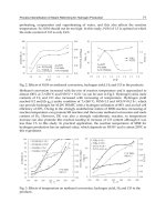
Calculations carried out for the case of a film thickness d = 5 µm which is often used in the
fabrication of CdTe-based solar cells and a typical carrier lifetime of 10
–9
-10
–10
s (Sites et al.,
2007) in thin-film CdTe/CdS solar cells show that the maximum value of J
sc
≈ 25-26 mA/cm
2
(Fig. 8(b)) is obtained when the concentration of noncompensated acceptors is N
a
– N
d
=
10
15
-10
16
cm
–3
. Therefore, in the following calculations a photocurrent density J
sc
≈ 26
mA/cm
2
will be used.
In Fig. 12(a) the calculated I-V characteristics of the CdS/CdTe heterojunction under
illumination are shown. The curves have been calculated by Eq. (30) using Eqs. (25), (28),
(29) for
τ
=
τ
no
=
τ
po
= 10
–9
s, N
a
– N
d
= 10
16
cm
–3
and various resistivities of the p-CdTe layer.
As is seen, an increase in the resistivity
ρ
of the CdTe layer leads to decreasing the open-
circuit voltage V
oc
. As
ρ
varies, Δ
μ
also varies affecting the value of the recombination
current, and especially the over-barrier current. The shape of the curves also changes
affecting the fill factor FF which can be found as the ratio of the maximum electrical power
to the product J
sc
V
oc
(Fig. 12(a)). Evidently, the carrier lifetime
τ
n
also influences the I-V
characteristic of the heterojunction under illumination. In what follows the dependences of
these characteristics on
ρ
and
τ
are analyzed.
The dependences of open-circuit voltage, fill factor and efficiency on the carrier lifetime
calculated at different resistivities of the CdTe absorber layer are shown in Fig. 13. As is
seen, V
oc
considerably increases with lowering
ρ
and increasing
τ
. In the most commonly
encountered case, as
τ
= 10
–10
-10
–9
s, the values of V
oc
= 0.8-0.85 V are far from the maximum
possible values of 1.15-1.2 V, which are reached on the curve for
ρ
= 0.1 Ω⋅cm and
τ
> 10
–8
.
A remarkable increase of V
oc
is observed when
ρ
decreases from 10
3
to 0.1 Ω⋅cm.
Efficiency of Thin-Film CdS/CdTe Solar Cells
125
0 0.2 0.4 0.6 0.8 1.0
3
2
1
ρ
=10
3
Ω⋅cm
10 Ω⋅cm
0.1 Ω⋅cm
V (V)
J (A/cm
2
)
τ
= 10
–9
s
(a)
20
15
10
5
0 0.2 0.4 0.6
0.8
1.0
ρ
=10
3
Ω
⋅cm
10
Ω
⋅
cm
0.1
Ω
⋅
cm
V (V)
P (mW/cm
2
)
τ
= 10
–9
s
(b)
Fig. 12. I-V characteristics (a) and voltage dependence of the output power (b) of CdS/CdTe
heterojunction under АМ1.5 solar irradiation calculated for J
sc
= 26 mA/cm
2
,
τ
= 10
–9
s
and different resistivities
ρ
of the CdTe absorber layer.
Fig. 13(b) illustrates the dependence of the fill factor FF = P
max
/(J
sc
⋅V
oc
) on the parameters of
the CdS/CdTe heterostructure within the same range of
ρ
and
τ
(P
max
is the maximal output
power found from the illuminated I-V characteristic). As it is seen, the fill factor increases
from 0.81-0.82 to 0.88-0.90 with the increase of the carrier lifetime from 10
–11
to 10
–7
s. The
non-monotonic dependence of FF on
τ
for
ρ
= 0.1 Ω⋅cm is caused by the features of the I-V
characteristics of the CdS/CdTe heterostructures, namely, the deviation of the I-V
dependence from exponential law when the resistivity of CdTe layer is low (see Fig. 11,
V > 0.8 V).
Finally, the dependences of the efficiency
η
= P
out
/P
irr
on the carrier lifetime
τ
n
calculated
for various resistivities of the CdTe absorber layer are shown in Fig. 13(c), where P
irr
is the
AM 1.5 solar radiation power over the entire spectral range which is equal to 100 mW/cm
2
(Standard IOS, 1992). As it is seen, the value of
η
remarkably increases from 15-16% to 21-
27.5% when
τ
and
ρ
changes within the indicated limits. For
τ
= 10
–10
-10
–9
s, the efficiency
lies near 17-19% and the enhancement of
η
by lowering the resistivity of CdTe layer is 0.5-
1.5% (the shaded area in Fig. 13(c)).
Thus, assuming
τ
= 10
–10
-10
–9
s, the calculated results turn out to be quite close to the
experimental efficiencies of the best samples of thin-film CdS/CdTe solar cells (16-17%).
The conclusion followed from the results presented in Fig. 13(c) is that in the case of a
CdS/CdTe solar cell with CdTe thickness 5 μm, enhancement of the efficiency from 16-17%
to 27-28% is possible if the carrier lifetime increases to
τ
≥ 10
–6
s and the resistivity of CdTe
reduces to
ρ
≈ 0.1
Ω⋅cm. Approaching the theoretical limit
η
= 27-28% requires also an
increase in the short-circuit current density. As it is follows from section 3.3, the latter is
possible for the thickness of the CdTe absorber layer of 20-30 μm and more.
Solar Energy
126
(c)
0.14
0.16
0.18
0.20
0.22
0.24
0.26
0.28
10
–11
10
–6
10
–9
10
–10
τ
(s)
10
–7
10
–8
η
ρ
= 0.1 Ω
⋅
cm
10
2
1.0
10
10
3
FF
0.82
0.84
0.86
0.88
0.80
0.90
ρ
= 0.1 Ω
⋅
cm
10
2
1.0
10
10
3
(b)
0.7
0.8
0.9
1.1
1.2
1.0
(a)
ρ
= 0.1 Ω
⋅
cm
10
2
1.0
10
10
3
V
oc
(V)
Fig. 13. Dependences of the open-circuit voltage V
oc
(a), fill factor FF (b) and efficiency
η
(c)
of CdS/CdTe heterojunction on the carrier lifetime τ calculated by Eq. (30) using Eqs. (24)-
(29) for various resistivities
ρ
of the CdTe layer. The experimental results achieved for the
best samples of thin-film CdS/CdTe solar cells are shown by shading.
Efficiency of Thin-Film CdS/CdTe Solar Cells
127
6. Conclusion
The findings of this paper give further insight into the problems and ascertain some
requirements imposed on the CdTe absorber layer parameters in a CdTe/CdS solar cell,
which in our opinion could be taken into account in the technology of fabrication of solar
cells.
The model taking into account the drift and diffusion photocurrent components with regard
to recombination losses in the space-charge region, at the CdS-CdTe interface and the back
surface of the CdTe layer allows us to obtain a good agreement with the measured quantum
efficiency spectra by varying the uncompensated impurity concentration, carrier lifetime
and surface recombination velocity. Calculations of short-circuit current using the obtained
efficiency spectra show that the losses caused by recombination at the CdTe-CdS interface
are insignificant if the uncompensated acceptor concentration N
a
– N
d
in CdTe is in excess of
10
16
cm
–3
. At N
a
– N
d
≈ 10
16
cm
–3
and the thickness of the absorbing CdTe layer equal to
around 5 µm, the short-circuit current density of 25-26 mA/cm
2
can be attained. As soon as
N
a
– N
d
deviates downward or upward from this value, the short-circuit current density
decreases significantly due to recombination losses or reduction of the photocurrent
diffusion component, respectively. Under this condition, recombination losses in the space-
charge region can be also neglected, but only when the carrier lifetime is equal or greater
than 10
–10
s.
At N
a
– N
d
≥ 10
16
cm
–3
, when only a part of charge carriers is generated in the neutral part of
the p-CdTe layer, total charge collection can be achieved if the electron lifetime is equal to
several microseconds. In this case the CdTe layer thickness d should be greater than that
usually used in the fabrication of CdTe/CdS solar cells (2-10 μm). However, in a common
case where the minority-carrier (electron) lifetime in the absorbing CdTe layer amounts to
10
–10
–10
–9
s, the optimum layers thickness d is equal to 3–4 μm, i.e., the calculations support
the choice of d made by the manufacturers mainly on an empirical basis. Attempts to reduce
the thickness of the CdTe layer to 1–1.5 μm with the aim of material saving appear to be
unwarranted, since this leads to a considerable reduction of the short-circuit’s current
density J
sc
and, ultimately, to a decrease in the solar-cell efficiency. If it will be possible to
improve the quality of the absorbing layer and, thus, to raise the electron lifetime at least to
10
–8
s, the value of J
sc
can be increased by 1–1.5 mA/cm
2
.
The Sah-Noyce-Shockley theory of generation-recombination in the space-charge region
supplemented with over-barrier diffusion flow of electrons provides a quantitative
explanation for all variety of the observed I-V characteristics of thin-film CdS/CdTe
heterostructure. The open circuit voltage V
oc
significantly increases with decreasing the
resistivity
ρ
of the CdTe layer and increasing the effective carrier lifetime
τ
in the space
charge region. At
τ
= 10
–10
-10
–9
s, the value of V
oc
is considerably lower than its maximum
possible value for
ρ
≈ 0.1 Ω⋅cm and
τ
> 10
–8
s and the calculated efficiency of a CdS/CdTe
solar cell with a CdTe layer thickness of 5 μm lies in the range 17-19%. An increase in the
efficiency and an approaching its theoretical limit (28-30%) is possible in the case when
the electron lifetime
τ
n
≥ 10
–6
s and the thickness of CdTe absorber layer is 20-30 μm or more.
The question of whether an increase in the CdTe layer’s thickness is reasonable under the
conditions of mass production of solar modules can be answered after an analysis of
economic factors.
Solar Energy
128
7. Acknowledgements
I thank X. Mathew, Centro de Investigacion en Energia-UNAM, Mexico, for the CdS/CdTe
thin-film heterostructures for measurements, V.M. Sklyarchuk for sample preparation to
study, V.V. Motushchuk and E.V. Grushko for measurements carried out, and all
participants of the investigation for helpful discussion. The study was supported by the
State Foundation for Fundamental Investigations (Ministry of Education and Science,
Ukraine) within the Agreement Φ14/259-2007.
8. References
Acrorad Co, Ltd., 13-23 Suzaki, Gushikawa, Okinawa 904-2234, Japan. Available:
Aramoto T., Kumazawa S., Higuchi H., Arita T., Shibutani S., Nishio T., Nakajima J., Tsuji
M., Hanafusa A., Hibino T., Omura K., Ohyama H. &, Murozono M., (1997). 16.0%
Efficient Thin-Film CdS/CdTe Solar Cells. J. Appl. Phys. 36, 6304-6305.
Baldazzi G., Bollini D., Casali F., Chirco P., Donati A., Dusi W., Landini G., Rossi M. &
Stephen J. B., (1993). Timing response of CdTe detectors, Nucl. Instr. and Meth. A326
319-324.
Birkmire, R.W. & Eser, E. (1997). Polycrystalline thin film solar cells: Present status and
future potential, Annu. Rev. Mater. Sc. 27, 625.
Britt, J. & Ferekides, С., (1993), Thin-film CdS/CdTe solar cell with 15.8% efficiency. Appl.
Phys. Lett. 62, 2851-2853.
Bonnet, D. (2001). Cadmium telluride solar cells. In: Clean Electricity from Photovoltaic. Ed.
by M.D. Archer, R. Hill. Imperial College Press, pp. 245-276.
Bonnet, D. (2003). CdTe thin-film PV modules, In: Practical Handbook of Photovoltaic:
Fundamentals and Applications. Ed. by T. Makkvart and L. Castaner. Elseivier,
Oxford.
Compaan A.D., Sites J.R., Birkmire R.W., Ferekides C.S. and Fahrenbruch A.L. (1999).
Critical Issues and Research Needs for CdTe-Based Solar Cells, Proc. 195th Meeting
of the Electrochemical Society), PV99-11, Seattle, WA, pp. 241-249.
Demtsu S.H. & Sites J.R., (2005). Quantification of losses in thin-film CdS/CdTe solar cells,
Proc. 31rd IEEE Photovoltaic Specialists Conf. pp. 3-7, Florida, Jan. 347-350.
Desnica, U.V., Desnica-Frankovic I.D., Magerle R., Burchard A. & Deicher M (1999).
Experimental evidence of the self-compensation mechanism in CdS, J. Crystal
Growth, 197, 612-615.
Eizen Y. (1992). Current state-of-the-art applications utilizing CdTe derectors, Nucl. Instr.
and Meth. A322, 596-603.
Ferekides, C.S., Balasubramanian, U., Mamazza, R., Viswanathan, V., Zhao, H. & Morel,
D.L. (2004) CdTe thin-film solar cells: device and technology issues, Solar Energy 77,
823-830.
Fritsche, J., Kraft, D., Thissen, A., Mayer, Th., Klein & A., Jaegermann W. (2001). Interface
engineering of chalcogenide semiconductors in thin film solar cells: CdTe as an
example, Mat. Res. Soc. Symp. Proc. , 668, 601-611.
Gartner W.W., (1959). Depletion-layer photoeffects in semiconductors, Phys. Rev. 116, 84-87.
Efficiency of Thin-Film CdS/CdTe Solar Cells
129
Goetzberger, A. , Hebling, C. & Schock, H W. (2003). Photovoltaic materials, history, status
and outlook, Materials Science and Engineering R40, 1-46.
Grasso, C., Ernst, K., R. Könenkamp, Lux-Steiner, M.C. & Burgelman, M. (2001).
Photoelectrical Characterisation and Modelling of the Eta-Solar Cell. Proc. 17th
European Photovoltaic Solar Energy Conference, vol. 1. pp. 211-214, Munich, Germany,
22-26 October.
Hanafusa, A., Aramoto, T., Tsuji, M., Yamamoto, T., Nishio, T., Veluchamy, P., Higuchi, H.,
Kumasawa, S., Shibutani, S., Nakajima, J., Arita T., Ohyama, H., Hibino T., Omura
& K. (2001). Highly efficient large area (10.5%, 1376 cm2) thin-film CdS/CdTe solar
cell, Solar Energy Materials & Solar Cells. 67, 21-29.
Holliday D. P., Eggleston J. M. and Durose K., (1998). A photoluminescence study of
polycrystalline thin-film CdTe/CdS solar cells. J. Cryst. Growth. 186, 54-549.
Kosyachenko, L.A., Sklyarchuk, V.M. , Sklyarchuk, Ye.F. & Ulyanitsky, K.S. (1999). Surface-
barrier p-CdTe-based photodiodes, Semicond. Sci. Technol., 14, 373-377.
Kosyachenko L.A., Rarenko I.M., Zakharuk Z.I., Sklyarchuk V.M., Sklyarchuk Ye.F.,
Solonchuk I.V., Kabanova I.S. & Maslyanchuk E.L. (2003). Electrical properties of
CdZnTe surface-barrier diodes. Semiconductors. 37, 238-242.
Kosyachenko L.A., Mathew X., Motushchuk V.V. & Sklyarchuk V.M. (2005). The generation-
recombination mechanism of charge transport in a thin-film CdS/CdTe
heterojunction, Semiconductors, 39, 539–542.
Kosyachenko, L.A. (2006). Problems of Efficiency of Photoelectric Conversion in Thin-Film
CdS/CdTe Solar Cells, Semiconductors. 40, 710-727.
Lavagna, M., Pique, J.P. & Marfaing, Y. (1977). Theoretical analysis of the quantum
photoelectric yield in Schottky diodes, Solid State Electronics, 20, 235-240.
Mathew, X., Kosyachenko, L.A., Motushchuk, V.V. & Sklyarchuk. O.F. (2007). Requirements
imposed on the electrical properties of the absorbed layer in CdTe-based solar cells.
J. Materials Science: Materials in Electronics. 18, 1021-1028.
McCandless, B.E., Hegedus, S.S., Birkmire, R.W. & Cunningham, D. (2003). Correlation of
surface phases with electrical behavior in thin-film CdTe. devices. Thin Solid Films
431–432, 249-256.
Meyers, P.V. & Albright, S.P. (2000). Photovoltaic materials, history, status and outlook.
Prog. Photovolt.: Res. Appl. 8, 161- 168.
Phillips J.I., Brikmire R.W., McCandless B.E., Mayers P.V. & Shaparman W.N., (1996).
Polycrystalline heterojunction solar cells: a device perspective. Phys. Stat. Sol. (b) 31,
31-39.
Reference solar spectral irradiance at the ground at different receiving conditions. Standard
of International Organization for Standardization ISO 9845-1:1992.
Romeo, N., Bosio, Canevari, A. V. & Podesta A., (2004). Recent progress on CdTe/CdS thin
film solar cells, Solar Energy , 77, 795-801.
Sah C., Noyce R. & Shockley W. (1957). Carrier generalization recombination in p-n
junctions and p-n junction characteristics, Proc. IRE. 45, 1228–1242.
Sites, J.R. & Xiaoxiang Liu, (1996). Recent efficiency gains for CdTe and CuIn
1−x
Ga
x
Se2 solar
cells: What has changed? Solar Energy Materials & Solar cells. 41/42 373-379.
Solar Energy
130
Sites J.R. & Pan J., (2007). Strategies to increase CdTe solar-cell voltage. Thin Solid Films, 515,
6099-6102.
Surek, T. (2005). Crystal growth and materials research in photovoltaics: progress and
challenges, Journal of Crystal Growth. 275, 292-304.
Sze, S. (1981). Physics of Semiconductor Devices, 2nd ed. Wiley, New York.
Toshifumi, T., Adachi, S., Nakanishi, H. & Ohtsuka M. (993). K. Optical constants of
Zn1-xCdxTe Ternary alloys: Experiment and Modeling. Jpn. Appl. Phys. 32, 3496-
3501.
Wu, X., Keane, J.C., Dhere, R.G., Dehart, C., Albin, D.S., Duda, A., Gessert, T.A., Asher, S.,
Levi, D.H. & Sheldon, P. (2001). 16.5%-efficient CdS/CdTe polycrystalline thin-film
solar cell, In: Proceedings of the 17th European Photovoltaic Solar Energy Conference,
Munich, Germany, October 2001, p. 995-1000.
7
Energy Control System
of Solar Powered Wheelchair
Yoshihiko Takahashi, Syogo Matsuo, and Kei Kawakami
Department of Mechanical System Engineering
Department of Vehicle System Engineering
Kanagawa Institute of Technology
Japan
1. Introduction
Independence is a major concern for individuals with severe handicaps. Welfare assistance
robotic technology is a popular solution to this concern (e.g. Hashino, 1996; Takahashi,
Ogawa, and Machida, 2002 and 2008). Assistance robotic technologies offer potential
alternatives to the need for human helpers. People bound to wheelchairs have limited
mobility reliant on battery life, which only allows for short distance travel between charges.
In addition, recharging batteries is time consuming.
Hydrogen
tank
Battery
Photovoltaic
(a) Abundant sun light (b) Solar energy not available
Fig. 1. Running conditions of proposed robotic wheelchair
The aim of this paper is to propose a system which will increase the moving distance of an
electrical wheelchair by adding two solar powered energy sources; a small photovoltaic cell
and a fuel cell. Fig.1 displays the running conditions of the proposed robotic wheelchair.
The control system will ideally give priority to the photovoltaic cell, next to the fuel cell and
finally to the battery. When sufficient sun light is available, the photovoltaic cell on the
wheelchair roof is used, when it is limited, the fuel cell or the battery is used. The energy
control system is designed using a micro computer, and the energy source is quickly
Solar Energy
132
changeable. Our objective is that the proposed robotic solar wheelchair will enable users to
enjoy increased independence when they are outdoors.
The advantage of using a solar powered energy source is that it produces power without
requiring use of fossil fuels. A photovoltaic cell is installed on the roof of the wheelchair,
which produces enough power to operate the apparatus when enough sun light is available.
The battery is charged using a large photovoltaic cell on the roof of the setup. Hydrogen is
produced using a water electrolysis hydrogen generator, and the fuel cell utilizes the
produced hydrogen. The large photovoltaic cell also sends electricity to the hydrogen
generator.
Photovoltaic cells and fuel cells are representative sustainable technologies (Bialasiewicz,
2008; Okabe et al., 2009; KE Jin et al., 2009). We are able to use two methods to produce
hydrogen using these sustainable technologies for our wheelchair. The first method is to
generate hydrogen from the electrolysis of water. The next is to use waste biomass which
produces biomass ethanol. Hydrogen is produced by steam reforming the ethanol
(Takahashi, & Mori, 2006; Essaki et al., 2008; Saxena et al., 2009; Rubin, 2008; Sugano, &
Tamiya, 2009). Standard sized fuel cell models are developed with the aim to develop a
commercially viable vehicle (Tabo et al., 2004; Kotz, et al., 2001; Rodatz, et al., 2001). Hybrid
vehicles using photovoltaic cells and fuel cells are developed in two universities (Konishi, et
al., 2008; Obara, 2004). Small fuel cell vehicles were developed (Nishimura, 2008; Takahashi,
2009a and 2009b). A wheelchair with a fuel cell has been developed (Yamamuro, 2003).
This paper will present a robotic wheelchair using solar powered energy sources of the
photovoltaic and fuel cell, detail the energy flow concept for charging electricity to the
battery and for storing hydrogen to the tank, the mechanical construction, the energy
control system, and the experimental results of the running test.
2. Energy flow of proposed robotic wheelchair
A schematic explanation and block diagram of the energy flow used in the proposed robotic
wheelchair are shown in Figs. 2 and 3. The energy system used in the robotic wheelchair
does not exhaust carbon dioxide as it does not utilize fossil fuels.
The first energy flow line in the schematic diagrams is the line from the photovoltaic cells on
the roof of the wheelchair. A cascade connection of two photovoltaic cells (Kyosera, KC-
40TJ) of 17.4 V and 43 W in nominal value is utilized as the energy source. The output
voltage is reduced to 24 V using a DC-DC converter.
The second energy line is the line from the water electrolysis hydrogen generator. The
photovoltaic cell on the setup roof (approximately 10 kW) sends electricity to the water
electrolysis hydrogen generator. The generated hydrogen is stored in a metal hydride
hydrogen tank of 60 NL. The output pressure of the hydrogen generator is approximately
0.3 MPa. The hydrogen tanks are installed on the wheelchair body after storing hydrogen. A
metal hydride tank is used for safety concerns. A fuel cell (Daido Metal, HFC-24100)
producing 24 V and 100 W in nominal values is used to generate electricity to the motor.
The third energy flow line is the battery line. The battery is charged with electricity from the
photovoltaic cell producing approximately 10 kW on the setup roof, and then installed on
the wheelchair body.
The fourth energy flow line is the biomass line. Ethanol is produced from waste biomass.
Hydrogen is then generated from the ethanol using a steam reforming hydrogen generator.
The generated hydrogen is stored in a 60 NL metal hydride hydrogen tank. The hydrogen
Energy Control System of Solar Powered Wheelchair
133
Photovoltaic
Hydrogen
generator
(Water electrolysis)
Hydrogen
tank
HydrogenBattery
Electricity
Photovoltaic
Hybrid wheelchair
Hydrogen
generator
(Steam reforming)
Waste biomass
Solar energy
Sun
Biomass ethanol
production
Fig. 2. Schematic explanation of energy flow
tanks are installed on the wheelchair body in the same manner as the second line. Ethanol is
safe to handle, and is easy to carry, however, the fourth energy flow line is still a matter
under consideration.
The High-Tech Research Center Project for Solar Energy System at the Kanagawa Institute
of Technology is conducting research on applications of solar energy. The development of
the robotic wheelchair is conducted as a part of the High-Tech Research Center Project. The
battery charging and hydrogen storing to the metal hydride are conducted using the facility
at the High-Tech Research Center Project.
3. Mechanical construction
Fig. 4 displays the fabricated robotic wheelchair with the photovoltaic and fuel cell. A
reinforced YAMAHA JW-1 wheelchair was used as the main body of the experimental set
up. In this configuration, the photovoltaic cell, the fuel cell, and the battery are installed on
the top, on the back, and under the wheelchair, respectively. The energy control system and
Solar Energy
134
10kW
Photovoltaic
Electricity
Hydrogen
Generator
(Water electrolysis)
Hydrogen
tank
Battery
Electricity
Hydrogen
tank
Battery
86W
Photovoltaic
100W
Fuel cell
Motor system
Energy control
system
Hybrid wheelchair
Hydrogen
Generator
(Steam reforming)
Hydrogen
Biomass ethanol
productuin
Waste biomass
Fig. 3. Block diagram of energy flow
PhotovoltaicIllumination sensor
Joy stickMotor unit
Hydrogen
tank
Energy control
system
Battery Fuel cell
Fig. 4. Fabricated robotic wheelchair with photovoltaic and fuel cell
hydrogen tanks are installed on the back of the wheelchair. Figs.5 (a) and (b) show the
photovoltaic and illumination sensor. Fig.6 (a) exhibits the fuel cell (Daido Metal, HFC-
24100) and the vibration isolator. Fig.6 (b) shows the metal hydride tanks of 60 NL and 0.3
Energy Control System of Solar Powered Wheelchair
135
MPa. The hydrogen pressure is adjusted to 0.08 MPa using a regulator. The main
specifications are as follows.
Wheelchair mechanism (Yamaha, JW-1)
Weight : 13 kg
Running operation : Joy stick
Motor : DC24V, 90Wx2
Photovoltaic (Kyosera, KC-40TJ)
Type : Multi crystal
Nominal power : 43 W
Maximum voltage : 17.4 V
Dimensions : 526x652x54 mm
Weight : 4.5 kg
Fuel cell (Daido Metal, HFC-24100)
Nominal power : 100 W
Nominal voltage : 24 V
Dimensuions : 160x110x240 mm
Weight : 3 kg
Air fans : DC24, 0.94Wx 24
(a) Photovoltaic (b) Illumination sensor
Fig. 5. Photovoltaic and illumination sensor
(a) Fuel cell and vibration isolator (b) Hydrogen tank and regulator
Fig. 6. Fuel cell and hydride tank
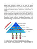
4. Energy control system
Fig.7 shows the concept of the energy control system where a micro computer determines
the wheelchair condition, and selects the optimum energy source from the three energy
sources: the photovoltaic on the wheelchair roof; the fuel cell; or the battery. Solid lines
Solar Energy
136
indicate energy flow lines, and dotted lines indicate the control signal flow lines. Fig.8
displays energy control architecture in detail. The switching control system inputs the
voltages of the photovoltaic cell, the fuel cell, and the motor drive current, and selects the
energy source determined by the wheelchair condition.
BatteryFuel cellPhotovoltaic
Power line
Signal line
Switching
ON/OFF
Switching
ON/OFF
Switching
ON/OFF
Motor driver
Motor
Micro computer
Fig. 7. Concept of energy control system
Battery
100W
Fuel cell
86W
Photovotaic
Motor driver
Switching control
system
DC/DC
Converter
Motor
Current detection
Voltage detection
Voltage detection
Power line
Signal line
Fig. 8. Detailed energy control architecture
Fig.9 is the software control algorithm of the energy control system. Fig.10 shows the
fabricated switching control system of the energy control system where a micro computer
controls the entire energy control system, and FETs are used to switch the energy flow.
Performance of energy source switching is also tested as this is the first attempt to develop a
solar powered wheelchair. The electricity acquired from the photovoltaic cell on the
wheelchair roof will be utilized to charge with the battery. Instant power increase using a
Energy Control System of Solar Powered Wheelchair
137
capacitor will also be required. Improvement of the energy control system must be
addressed in future research.
The control system will ideally give priority to the photovoltaic cell then to the fuel cell and
then to the battery. Essentially, the switching control is conducted on the motor driving
current considering the condition of the photovoltaic and fuel cells. If the motor driving
current is below 2.5 A and the photovoltaic voltage is above 30 V, then the photovoltaic is
selected. If the motor driving current is below 4.0 A and the fuel cell voltage is above 24 V,
then the fuel cell is selected. When the motor driving current is below 20.0 A, then the
battery is selected. The following details the software control algorithm of the energy control
system.
0 < i <= 2.5 [A]
F
T
Photovoltaicvp >= 30 [V]
T
vf >= 24 [V]
Fuel cell
T
Battery
F
Motor current i input
Photovoltaic voltage vp input
Fuel cell voltage vf input
Start
T
2.5 < i <= 4 [A]
T
F
F
T
vf >= 24 [V]
Fuel cell
Battery
F
4 < i <= 20 [A]
F
Battery
Stop
(a)
(b)
(c)
(d)
(e)
(f)
Fig. 9. Software control algorithm of energy control system
Condition (a) :
When the motor current is over 0.0 A and less than 2.5 A,
and the photovoltaic voltage is over 30 V,
then the photovoltaic is selected.
Condition (b) :
When the motor current is over 0.0 A and less than 2.5 A,
and the photovoltaic voltage is less than 30 V,
and the fuel cell voltage is over 24 V,
then the fuel cell is selected.
Condition (c) :
When the motor current is over 0.0 A and less than 2.5 A,
and the photovoltaic voltage is less than 30 V,
and the fuel cell voltage is less than 24 V,
then the battery is selected.