Mobile and wireless communications network layer and circuit level design Part 7 docx
Bạn đang xem bản rút gọn của tài liệu. Xem và tải ngay bản đầy đủ của tài liệu tại đây (2.62 MB, 30 trang )
MicrostripAntennasforMobileWirelessCommunicationSystems 171
4.3-PIFA as compact multiband antenna
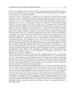
PIFA is well-known as terminal antenna design. These antennas offer reduced size over
traditional microstrip antennas because the resonance frequency is at about quarter wave
rather than at half wave in conventional ones due to the shorting pins/walls in its structure
as shown in figure 5 (T. Taga, 1992).
Fig 5. Comparison between conventional microstrip patch antenna and conventional PIFA
antenna
The selection of PIFA is due to certain advantages as
The PIFA bandwidth is affected very much by varying the size of the ground plane,
generally, reducing the ground plane can effectively broaden the bandwidth of the antenna
system.
PIFA impedance matching can be obtained by the correct positioning of feeding and
grounding pins. Thickness of the antenna and permittivity of the substrate material used
also affect the impedance of the feeding point. To shrink the size of the PIFA, high constant
dielectric substrate materials can be used. This weakens the performance of the antenna,
because dielectric material gathers electromagnetic fields and therefore it doesn't radiate as
good as the air insulated PIFA. Also part of the feed power goes into the dielectric losses of
the substrate material. The height of the PIFA is a very critical dimension since it has a great
effect on the antenna’s radiation and also its impedance bandwidth (J. Elling et al, 1991; C.
R. Rowell & R. D. Murch 1997). The basic rule is that the bigger the air gap between the
radiator and ground plane is, the better the gain and the broader the impedance bandwidth
will be. Table 3 summarizes the effect of different PIFA design parameters,(height, width,
length, location of feed and shorting pin/wall and size of the ground plane) on its
characteristics.
Parameters Effect
Height Control bandwidth
Width Control impedance matching
Length Increase inductance of the antenna and determine resonance
frequency
Width of short strip
Affect on the anti-resonance and increase bandwidth
Feed position fro
m
short strip
Affect on resonance frequency and bandwidth
Table 3. The effect of PIFA parameters on its characteristics
Shorting wall
4.4 PIFA structures for multiband and compact size applications:
4.4.1 Rectangular PIFA shape with U-shaped slots
A practical method to design a single feed multiband PIFA that covers both the cellular and
non cellular bands is developed (Dalia Nashaat et al, 2005; Hala Elsadek, 2005; R. Chair et al,
1999). From the commercial point of view, there are now different frequency bands for
portable cellular/non cellular devices as the conventional 0.9GHz GSM band for mobile
phones and 1.8GHz DCS band for wireless cellular applications. Furthermore the Bluetooth
wireless technology at 2.4 GHz is already applied in many portable devices and in most
wireless communication systems as mobile phones, laptops, PDAS, car stereos, audio
speakers, toys, etc (Bluetooth information web site). Moreover the band of WLAN at 5.2GHz
is being applied in some applications. The compact and multiband functionality is not the
only required demand in such antenna systems for wireless communication applications
but, also other characteristics should be satisfied as small size, light weight, omni directional
radiation pattern, reasonable gain and acceptable bandwidth.
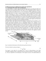
Quad band PIFA with single coaxial probe feeding is investigated. Foam substrate is used
for light weight, rigid structure and easy shielding purposes. Three U-shaped slots are
added with certain dimensions and at appropriate positions for operation at the
aforementioned four frequency bands. The size reduction is 30% from conventional quarter
wavelength PIFA. Additional reduction by 15% is achieved by adding a capacitance load in
the vertical direction. The impedance bandwidth is fairly acceptable. The antenna gain is
satisfactory and the radiation pattern is quasi isotropic at the respective four bands of
interest. The proposed concept of adding U-shaped slots is a distinct advantage of the
design since the bands of operation are independent on each other except the small
controllable mutual coupling between the slots. Figure 6 illustrates the suggested antenna
design.
Fig. 6. Geometrical dimensions of the fabricated quad band antenna
The rule of thumb in antenna design is:
)(4
ii
i
WL
c
f
(4)
The length L
i
and width W
i
are replaced by L
1
and W
1
=(61mm,40mm) of the PIFA
rectangular radiating surface to determine the first resonance frequency f
1
(0.9GHz). While,
(L
i
, W
i
) are replaced by the dimensions of the largest U-slot (L
2
, W
2
)=(23mm,30mm) to
(
a
)
L
L
1
Ground
Plane
W
1
h
Shorting
wall
Capacitor
plate
W
W
c
L
c
G
4
G
3
G
2
Probe
feed
Slots' width
G
1
MobileandWirelessCommunications:Networklayerandcircuitleveldesign172
generate the second resonance frequency f
2
(1.8GHz). They are also replaced by the length
(L
3,
W
3
)=(18mm,20mm)of the middle U-slot to get the third resonance frequency f
3
(2.45GHz). Finally, (L
i
, W
i
) are replaced by (L
4
,W
4
)=(9.5mm,8mm) of the smallest U-slot to
have the fourth resonance frequency at f
4
(5.2GHz). This multi-band antenna has
approximately the same size as a single-band PIFA operating at the lowest frequency band.
The radiating element is grounded with a shorting wall. It is found that the widest
bandwidth is achieved when the width of this wall is equal to the width of the PIFA
radiating plate. The antenna is fed using coaxial cable at the appropriate matching point for
the four bands of operation. The antenna impedance can be matched to 50Ω by controlling
the distance between the feed point and the shorting wall. The PIFA antenna is fabricated on
a foam substrate with dielectric constant ε
r
=1.07 in order to have rigid structure that can be
easily shielded. Adding U-slots on the PIFA radiating surface, reduces its size by about 30%
from the conventional PIFA shape. For further reduction in size, a capacitor plate load is
added between the radiating surface and the ground plane. This increases the reduction in
size to be about 45%.
The results of the structure simulations as well as experimental
measurements are illustrated in following three figures.
Fig. 9. The simulated radiation pattern of quad-band PIFA with 10PF shorting capacitor
plate at four different resonating frequencies, a) at parallel E-plane at phi=0 and b) at
perpendicular H-plane at phi=90.
Fig. 7. Comparison between measured and
simulated reflection coefficients of quad band
PIFA with three U-shaped slots at operating
frequencies of 0.95, 1.8, 2.45 and 5.2GHz,
respectively.
1 2 3 4 5 6
-35
-30
-25
-20
-15
-10
-5
0
Return loss of PIFA
with Quad-band
simulated
measured
Return Loss in dB
Frequency in GHz
Fig. 8. The relation between capacitor
load in PF and antenna percentage
reduction ratio compared to
conventional PIFA.
0 2 4 6 8 10
0
5
10
15
20
25
30
The relation between capacitance
load and reduction ratio
Reduction ratio (%)
Capacitance load (PF)
(
a
)
(b)
-50
-40
-30
-20
-10
0
0
30
60
90
120
150
180
210
240
270
300
330
-50
-40
-30
-20
-10
0
H-Plane
at 0.9GHZ
at 1.8GHz
at 2.45GHz
at 5.25GHz
-50
-40
-30
-20
-10
0
0
30
60
90
120
150
180
210
240
270
300
330
-50
-40
-30
-20
-10
0
E-Plane
at 0.9GHz
at 1.8GHz
at 2.45GHz
at 5.2GHz
MicrostripAntennasforMobileWirelessCommunicationSystems 173
generate the second resonance frequency f
2
(1.8GHz). They are also replaced by the length
(L
3,
W
3
)=(18mm,20mm)of the middle U-slot to get the third resonance frequency f
3
(2.45GHz). Finally, (L
i
, W
i
) are replaced by (L
4
,W
4
)=(9.5mm,8mm) of the smallest U-slot to
have the fourth resonance frequency at f
4
(5.2GHz). This multi-band antenna has
approximately the same size as a single-band PIFA operating at the lowest frequency band.
The radiating element is grounded with a shorting wall. It is found that the widest
bandwidth is achieved when the width of this wall is equal to the width of the PIFA
radiating plate. The antenna is fed using coaxial cable at the appropriate matching point for
the four bands of operation. The antenna impedance can be matched to 50Ω by controlling
the distance between the feed point and the shorting wall. The PIFA antenna is fabricated on
a foam substrate with dielectric constant ε
r
=1.07 in order to have rigid structure that can be
easily shielded. Adding U-slots on the PIFA radiating surface, reduces its size by about 30%
from the conventional PIFA shape. For further reduction in size, a capacitor plate load is
added between the radiating surface and the ground plane. This increases the reduction in
size to be about 45%.
The results of the structure simulations as well as experimental
measurements are illustrated in following three figures.
Fig. 9. The simulated radiation pattern of quad-band PIFA with 10PF shorting capacitor
plate at four different resonating frequencies, a) at parallel E-plane at phi=0 and b) at
perpendicular H-plane at phi=90.
Fig. 7. Comparison between measured and
simulated reflection coefficients of quad band
PIFA with three U-shaped slots at operating
frequencies of 0.95, 1.8, 2.45 and 5.2GHz,
respectively.
1 2 3 4 5 6
-35
-30
-25
-20
-15
-10
-5
0
Return loss of PIFA
with Quad-band
simulated
measured
Return Loss in dB
Frequency in GHz
Fig. 8. The relation between capacitor
load in PF and antenna percentage
reduction ratio compared to
conventional PIFA.
0 2 4 6 8 10
0
5
10
15
20
25
30
The relation between capacitance
load and reduction ratio
Reduction ratio (%)
Capacitance load (PF)
(
a
)
(b)
-50
-40
-30
-20
-10
0
0
30
60
90
120
150
180
210
240
270
300
330
-50
-40
-30
-20
-10
0
H-Plane
at 0.9GHZ
at 1.8GHz
at 2.45GHz
at 5.25GHz
-50
-40
-30
-20
-10
0
0
30
60
90
120
150
180
210
240
270
300
330
-50
-40
-30
-20
-10
0
E-Plane
at 0.9GHz
at 1.8GHz
at 2.45GHz
at 5.2GHz
4.4.2 Compact PIFA size with E-shaped radiator
Ultra compact PIFA with dual band resonant frequencies are investigated (Hala Elsadek,
2006). The antenna is designed and fabricated on both foam and FR4 cheap substrates with
dielectric constants
r
= 1.07 and 4.7, respectively. Over 95% reduction in the antenna size
is achieved from conventional
0
/4 rectangular PIFA resonating at same frequencies. This is
done by implementing two oppositely shorting capacitive straps under the radiating
surface. Dual band operation is achieved by inserting two parallel slots on the edges of the
PIFA radiating surface forming an E-shape. In this case, the center wing resonates at the
higher frequency while the two side wings resonate at the lower frequency. The antenna
resonance frequencies on FR4 substrate are 1.07GHz and 2.77 GHz with areas' reduction
ratios of 97% and 81% for the lower and upper resonance frequencies, respectively. The
antenna size on FR4 substrate is 13 x 11 x 8mm
3
. The antenna directivity is 3.73 with
radiation efficiency 97%. The radiation pattern has acceptable shape with low cross
polarization in both resonances and at both E-plane and H-plane directions. It is worth to
mention that, with frequency scaling, the same antenna structure can resonate at 2.4GHz
and 5.2GHz with dimensions 8mmx8mmx8mm Figure 10 shows the antenna geometry,
while figure 11 illustrates a comparison between simulated and measured results with
capacitive load reduction effect. There are different approaches for multiband compact
antenna design; however, we concentrated on PIFA with shorting plates and capacitive
loads with different radiator shapes. Since these shapes give excellent results for antenna
candidates in mobile communications.
(a) (b)
Fig. 11. Photo of fabricated E-shaped PIFA on commercial FR4 substrate and (b) comparison
between simulated and measured antenna reflection coefficients.
L
Ground
Plane
W
h
3
Shorting
wall
Capacitor
plate
Probe
feed
L
1
L
2
W
2
W
1
h
2
h
1
Fi
g
. 10. E-sha
p
ed PIFA antenna
g
eometr
y
.
0.5 1.0 1.5 2.0 2.5 3.0 3.5
-4 0
-2 0
0
Thre e layer E-shap ed PIFA
on FR4 substrate
simulated
m easured
S11 in dB
Frequency in GHz
MobileandWirelessCommunications:Networklayerandcircuitleveldesign174
5. Broad band and UWB Antennas
5.1- Introduction to broad band and UWB antennas
In last sections, we illustrate the challenge of small and multiband antenna that can fit in
several wireless communication systems at same time. In all previous designs, acceptable
antenna bandwidth was achieved. However, several other applications of wireless
communications require broadband and even ultawideband antenna rather than directional
one. Broad band antennas are desired for the increasing demand of communication
bandwidth that accommodates high data rate application like video-on-demand. Moreover
UWB technology attracts a lot of attention from the researchers in recent years because of
the various advantages it offers. UWB technology depends on transmitting pulses of width
in order of nano seconds instead of modulating sinusoidal signal and, hence broadening its
spectrum and tuning its power density beyond noise level (FCC, 2002). This method in
transmission exhibit many advantages as immunity to jamming and ability to combat fading
due to multipath effects. Also it has penetration capability as its spectrum include low
frequency components. Because of these advantages UWB technology has enormous
applications in wireless communications. One of the major application is the wireless sensor
network (WSN) which is useful in medical, tracking and localization applications (remote
sensing) (Ian Opperman at el., 2004; K.P. Ray, 2008). As UWB provide security and low
power consumption that increase the battery life of the portable terminals. On the other
hand, broad band communication systems as well as UWB technology faces a lot of
challenges as the radiation pattern stability and polarization purity along the whole band of
operation.
5.2-Different types of broad band antennas
Many designs have been investigated in literature for broadening the bandwidth of
antennas. This can be achieved by using different probe feeding shapes as L-shape, adding
parasitic elements to the radiator, folding the ground plane, etc. (Fan Yang, 2001; Yasshar
Zehforoosh, 2006). Taking in consideration for the stability of the beam pattern and
polarization purity along the bandwidth, the design quality is judged. Among the basic
ideas for broadening the band are inserting slots of different shapes (U,H,V) on the radiating
patch antenna to introduce longer current paths and hence add other staggered resonating
modes. The rule of thumb in adding another resonance to the antenna structure is the same
as that discussed in previous section for multiband antenna designs however, in case the
resonating modes are far from each other, the structure will act as multiband antenna. But if
the design is changed to let these resonances near from each other, they will complement
each other forming staggered resonating behavior and broadband antenna structure. Also
adding parasitic or stacked patch has been proposed in (Mohamed A. Alsharkawy at el.,
2004). Another types as aperture stacked and multi resonator stacked patches in (Ki-Hakkim
at el, 2006; Jeen Sheen Row, 2005) .In these types multi patch antenna are printed on
different layer forming multi resonators and hence broaden the antenna band. These types
are bulky and not adequate enough to be integrated with the modern wireless devices in
spite there are successful attempts for this. In addition they don’t exhibit enough bandwidth
to cover all wireless communication band nowadays (3.1-10.6GHz). Recently UWB slot
antenna in (Girish kumar, 2003; Yashar Zehforoosh at el, 2006) and printed monopole
antenna in (Soek H. Choi at el., 2004) are proposed. They attract a lot of interests due to their
MicrostripAntennasforMobileWirelessCommunicationSystems 175
5. Broad band and UWB Antennas
5.1- Introduction to broad band and UWB antennas
In last sections, we illustrate the challenge of small and multiband antenna that can fit in
several wireless communication systems at same time. In all previous designs, acceptable
antenna bandwidth was achieved. However, several other applications of wireless
communications require broadband and even ultawideband antenna rather than directional
one. Broad band antennas are desired for the increasing demand of communication
bandwidth that accommodates high data rate application like video-on-demand. Moreover
UWB technology attracts a lot of attention from the researchers in recent years because of
the various advantages it offers. UWB technology depends on transmitting pulses of width
in order of nano seconds instead of modulating sinusoidal signal and, hence broadening its
spectrum and tuning its power density beyond noise level (FCC, 2002). This method in
transmission exhibit many advantages as immunity to jamming and ability to combat fading
due to multipath effects. Also it has penetration capability as its spectrum include low
frequency components. Because of these advantages UWB technology has enormous
applications in wireless communications. One of the major application is the wireless sensor
network (WSN) which is useful in medical, tracking and localization applications (remote
sensing) (Ian Opperman at el., 2004; K.P. Ray, 2008). As UWB provide security and low
power consumption that increase the battery life of the portable terminals. On the other
hand, broad band communication systems as well as UWB technology faces a lot of
challenges as the radiation pattern stability and polarization purity along the whole band of
operation.
5.2-Different types of broad band antennas
Many designs have been investigated in literature for broadening the bandwidth of
antennas. This can be achieved by using different probe feeding shapes as L-shape, adding
parasitic elements to the radiator, folding the ground plane, etc. (Fan Yang, 2001; Yasshar
Zehforoosh, 2006). Taking in consideration for the stability of the beam pattern and
polarization purity along the bandwidth, the design quality is judged. Among the basic
ideas for broadening the band are inserting slots of different shapes (U,H,V) on the radiating
patch antenna to introduce longer current paths and hence add other staggered resonating
modes. The rule of thumb in adding another resonance to the antenna structure is the same
as that discussed in previous section for multiband antenna designs however, in case the
resonating modes are far from each other, the structure will act as multiband antenna. But if
the design is changed to let these resonances near from each other, they will complement
each other forming staggered resonating behavior and broadband antenna structure. Also
adding parasitic or stacked patch has been proposed in (Mohamed A. Alsharkawy at el.,
2004). Another types as aperture stacked and multi resonator stacked patches in (Ki-Hakkim
at el, 2006; Jeen Sheen Row, 2005) .In these types multi patch antenna are printed on
different layer forming multi resonators and hence broaden the antenna band. These types
are bulky and not adequate enough to be integrated with the modern wireless devices in
spite there are successful attempts for this. In addition they don’t exhibit enough bandwidth
to cover all wireless communication band nowadays (3.1-10.6GHz). Recently UWB slot
antenna in (Girish kumar, 2003; Yashar Zehforoosh at el, 2006) and printed monopole
antenna in (Soek H. Choi at el., 2004) are proposed. They attract a lot of interests due to their
low profile, ease of integration and very wide bandwidth. Next section will focus on the
UWB printed monopole antenna.
5.3- UWB antenna Design
Some considerations should be taken for UWB antenna design such (Hung-Jui Lam, 2005):
1-It should have bandwidth ranging from 3.1GHz to10.6GHz in which reasonable efficiency
is satisfactory.
2-In this ultra-wide bandwidth, an extremely low emission power level should be ensured.
(In 2002, the Federal Communication Commission (FCC) has specified the emission limits of
−41.3 dBm/MHz).
3-The antenna propagates short-pulse signal with minimum distortion over the frequency
range.
5.4 UWB Printed Monopole Antenna
Printed monopole antenna structure is shown in Figure 12 and it could be explained as an
evolution of the conventional microstrip antenna with ground plan eliminated (K.P. Ray,
2008). From the analysis of the microstrip antenna, (Hirasawa and K. Fujimoto, 1982; C.A.
Balanis, 1997) it is known that the substrate thickness (h) is directly proportional to the BW
and as (h) is extended to infinity by eliminating the ground plan the BW become very wide.
Also, the resonant frequency is function of the patch length, width and height. So when
patch printed on very thick substrate it excites higher order modes each enables broad
bandwidth case. If these higher order modes are close to each other the overall bandwidth is
ultrawideband. Another explanation for the printed monopole that it could be seen as
conventional monopole but with the cylindrical metallic rod flatted to be plane of any
different shapes (K.P. Ray, 2008) (rectangular, circular, elliptic)as it is known that impedance
bandwidth increase by increasing the diameter of the metallic rod. The printed plane that
alternate the metallic rod is considered of diameter extended to infinity exciting higher
order modes of large bandwidth. Upon optimizing the dimensions of the antenna, these
higher order modes could be close to each others to yield very broad bandwidth as will be
elaborated in next sections.
Fi
g
. 12. Geometr
y
of the rectan
g
ular
p
rinted mono
p
ole antenna
MobileandWirelessCommunications:Networklayerandcircuitleveldesign176
5.4.1 Analysis
As mentioned in previous section, printed monopole antenna is analog to the wire quarter
wave monopole antenna. This could be used to analytically design the antenna for the lower
edge frequency by equating its area (in this case rectangular monopole) to an equivalent
cylindrical monopole antenna of same height L and equivalent radius r as following:
2 rL WL
(5)
The input impedance of thin λ/4 monopole is half the input impedance of thin λ/2 dipole
and equal is slightly less than quarter wavelength and given by(15, 38)
0 24
1
0 24
30 0 24
72
L . λ K
where
K (L / r) / ( L / r) L / (L r)
(L r)
λ
.
therefore
c ( x . )
f / (L r) GHz
l
λ L r
(6)
Previous equation doesn’t account for the distance between the radiator and the ground
plane (h)
72 / ( )
l
f L r h GHz
(7)
where all dimensions are in millimeters. This analysis is valid for free space but in our case
where antenna is printed on a dielectric substrate which decrease the effectiveness of the
wavelength (λ
g
). Modification on the lower edge frequency is required and can be given by
72 / ( ) .
l
f
L r h k GHz
(8)
It is worthwhile to mention although previous analysis was on rectangular shape printed
monopole, it is valid on other various shapes of radiators but only L and r will differ
according to the geometry of the shape. (K. P. Ray, 2008).
After inspecting the lower edge frequency we need to control the bandwidth of the antenna.
Actually the L, r and h affects both lower edge frequency as well as the bandwidth too so
optimization is needed to give the required bandwidth as well as the lower frequency.
Another important thing that affects severely the bandwidth is the bottom shape of the
radiator in contact with the 50Ω feeder. As long as we avoid abrupt change in the
dimensions of the transition from the feeder to the radiator as long as we obtain broader
bandwidth. That’s why circular radiator inherent wider band than rectangular one. Abrupt
transition form feeder to radiator is overcome by using stepped or tapered feeders (S. I. Latif
at el., 2005; A.P. Zhao and J. Rahola, 2005). Finally using CPW (coplanar waveguide feed)
instead of microstrip feed enhances the bandwidth. As printed monopole antenna
resonating around quarter wave length so they have similar radiation pattern as normal
MicrostripAntennasforMobileWirelessCommunicationSystems 177
5.4.1 Analysis
As mentioned in previous section, printed monopole antenna is analog to the wire quarter
wave monopole antenna. This could be used to analytically design the antenna for the lower
edge frequency by equating its area (in this case rectangular monopole) to an equivalent
cylindrical monopole antenna of same height L and equivalent radius r as following:
2 rL WL
(5)
The input impedance of thin λ/4 monopole is half the input impedance of thin λ/2 dipole
and equal is slightly less than quarter wavelength and given by(15, 38)
0 24
1
0 24
30 0 24
72
L . λ K
where
K (L / r) / ( L / r) L / (L r)
(L r)
λ
.
therefore
c ( x . )
f / (L r) GHz
l
λ L r
(6)
Previous equation doesn’t account for the distance between the radiator and the ground
plane (h)
72 / ( )
l
f L r h GHz
(7)
where all dimensions are in millimeters. This analysis is valid for free space but in our case
where antenna is printed on a dielectric substrate which decrease the effectiveness of the
wavelength (λ
g
). Modification on the lower edge frequency is required and can be given by
72 / ( ) .
l
f
L r h k GHz
(8)
It is worthwhile to mention although previous analysis was on rectangular shape printed
monopole, it is valid on other various shapes of radiators but only L and r will differ
according to the geometry of the shape. (K. P. Ray, 2008).
After inspecting the lower edge frequency we need to control the bandwidth of the antenna.
Actually the L, r and h affects both lower edge frequency as well as the bandwidth too so
optimization is needed to give the required bandwidth as well as the lower frequency.
Another important thing that affects severely the bandwidth is the bottom shape of the
radiator in contact with the 50Ω feeder. As long as we avoid abrupt change in the
dimensions of the transition from the feeder to the radiator as long as we obtain broader
bandwidth. That’s why circular radiator inherent wider band than rectangular one. Abrupt
transition form feeder to radiator is overcome by using stepped or tapered feeders (S. I. Latif
at el., 2005; A.P. Zhao and J. Rahola, 2005). Finally using CPW (coplanar waveguide feed)
instead of microstrip feed enhances the bandwidth. As printed monopole antenna
resonating around quarter wave length so they have similar radiation pattern as normal
monopole. It is omni in the H-plane and eight shaped in the E-plane. Following are
examples about broad band and UWA antenna designs.
5.5 Examples on braodband and UWB microstrip antenna designs
5.5.1 Broad band antenna
The geometry of the proposed antennas is as shown in figure 13. The antenna consists of V-
shaped patch with V- unequal arms with dimensions (L
1
, W
1
) and (L
2
, W
2
). The isosceles
triangular antenna is with dimensions (L
T
, W
T
). The shorting wall width is equal to W
T
for
maximum size reduction (Hala Elsadek and Dalia Nashaat, 2008). The ground plane is with
rectangular shape of dimensions (L
g
, W
g
). The two parts of the structure, V-shaped patch
and triangular PIFA, are coupled through a V-shaped slot with unequal arms with slots’
lengths and widths are (L
s1
, W
s1
) and (L
s2
, W
s2
). The two arms of the V-shaped patch excite
TM
01
mode. The length of the two arms of the V-shaped patch is different in order to excite
two different staggered resonant modes. The unequal spacing/widths between the coaxially
fed triangular shorted patch and the V-shaped patch are for different values of coupling
thus, excite two more different modes. To add two more resonating modes, equal arms V-
shaped slot can be loaded on the triangular patch radiation surface. The substrate is foam
with dielectric constant
r
=1.07 and substrate height h=6mm. The antenna geometry is
illustrated in figure 13. When the ground plane size is reduced to certain proper value, the
antenna behavior changes to be wide bandwidth antenna rather than multiband antenna.
The resonating frequencies can be approximately determined from following equation
(Yujiang Wu and Zaiping Nie, 2007).
4
c
f
i
L
i
(9)
Where:
i
f
is resonant frequency at band i, C is the velocity of light =
8
103 m/s and
i
L is
the half length of the radiating surface or the length of the slot at the corresponding
operating band i. The Triangular PIFA part is excited by coaxial probe feed. The probe is
positioned in the centerline of the shorted patch at distance
f
d from shorting wall. The
f
d
value controls the antenna characteristics. For multiband operation, the resonating
frequencies are at 2.88GHz, 3.64GHz, 3.95GHz, 4.38GHz, 4.81GHz and 5.6GHz, the distance
f
d is 16.75mm while for broadband operation, the distance
f
d increased to be 18.5mm.
Figure 14 illustrates comparison between the simulated and measured results for the
multiband structure. The radiation pattern of the antenna is approximately omni directional
in both E-plane and H-plane with back to front ratio of less than 5dB and 3dB beamwidth of
about
60
.
Moving coaxial feeding towards open end of triangular PIFA antenna at
f
d = 18.5mm, the
resonant frequencies of the antenna become staggered close to each other so achieving
wideband operation. The bandwidth is 3% at the fundamental mode 2.95 GHz, hence the
fundamental resonating frequency will approximately not affected by changing the feed
MobileandWirelessCommunications:Networklayerandcircuitleveldesign178
position. The higher resonance bandwidth is 27% at 4.721GHz. Figure 15 presents the
comparison between the simulated and measured results of the wideband antenna
structure.
Folding the shorting wall of the triangular PIFA as in figure 13, converts the antenna to
UWB with bandwidth of 53% at same resonating frequency 4.65GHz. The antenna gain is
10.5 dBi
Fig. 14. Comparison between simulated and
measured results of the multi-band antenna
Fig. 15. Comparison between simulated
and measured results of broad band
antenna
5.5.2 UWB antenna
Consider we have substrate material of
r
=3.38 and h=0.813mm and we need to design
printed rectangular monopole shown in figure 12 so we need to know the values L,W,H for
obtaining lower edge resonance frequency at 5Ghz and obtain BW as Wide as possible.
From above equations in subsection 5.4.1, to satisfy 5GHz a lot of solutions could be
obtained for L, W, h but not all of them will give the maximum BW, so optimization is
Fig. 13. Configuration of the proposed antenna of V-shaped patch with unequal arms
cou
p
led to isosceles trian
g
ular PIFA throu
g
h V-sha
p
ed slot of une
q
ual arms
d
f
W
T
L
1
L
2
L
T
W
1
W
2
W
g
L
W
s1
L
L
s2
W
s2
Coaxial
feeding
Triangular
PIFA
V-shaped patch
with unequal arms
Ground plane
Folded shorting
wall for UWB
h
Shorting
wall
1 2 3 4 5 6
-35
-30
-25
-20
-15
-10
-5
0
reflection coefficient
simulated
measured
higher frequency bandwidth =27.3%
Return Loss in dB
Frequency in GHz
2 3 4 5 6
-35
-30
-25
-20
-15
-10
-5
0
Multi-band antenna configuration
simulated
measured
Return Loss in dB
Frequency GHz
MicrostripAntennasforMobileWirelessCommunicationSystems 179
position. The higher resonance bandwidth is 27% at 4.721GHz. Figure 15 presents the
comparison between the simulated and measured results of the wideband antenna
structure.
Folding the shorting wall of the triangular PIFA as in figure 13, converts the antenna to
UWB with bandwidth of 53% at same resonating frequency 4.65GHz. The antenna gain is
10.5 dBi
Fig. 14. Comparison between simulated and
measured results of the multi-band antenna
Fig. 15. Comparison between simulated
and measured results of broad band
antenna
5.5.2 UWB antenna
Consider we have substrate material of
r
=3.38 and h=0.813mm and we need to design
printed rectangular monopole shown in figure 12 so we need to know the values L,W,H for
obtaining lower edge resonance frequency at 5Ghz and obtain BW as Wide as possible.
From above equations in subsection 5.4.1, to satisfy 5GHz a lot of solutions could be
obtained for L, W, h but not all of them will give the maximum BW, so optimization is
Fig. 13. Configuration of the proposed antenna of V-shaped patch with unequal arms
cou
p
led to isosceles trian
g
ular PIFA throu
g
h V-sha
p
ed slot of une
q
ual arms
d
f
W
T
L
1
L
2
L
T
W
1
W
2
W
g
L
W
s1
L
L
s2
W
s2
Coaxial
feeding
Triangular
PIFA
V-shaped patch
with unequal arms
Ground plane
Folded shorting
wall for UWB
h
Shorting
wall
1 2 3 4 5 6
-35
-30
-25
-20
-15
-10
-5
0
reflection coefficient
simulated
measured
higher frequency bandwidth =27.3%
Return Loss in dB
Frequency in GHz
2 3 4 5 6
-35
-30
-25
-20
-15
-10
-5
0
Multi-band antenna configuration
simulated
measured
Return Loss in dB
Frequency GHz
needed for obtaining the optimum dimensions. Parametric analysis for the effects of these
three dimensions on bandwidth is shown in figures 16-18 (Hakim Aissat at el, 2006; Min
Hau Ho at el, 2005). Starting with L=W=0.25λ
0
/√
r
=8mm and h=2mm. From the three
figures below, the optimum dimensions are W=12,L=11.5 and H=0.75.
Fig. 16. The effect of
changing W on the return
Loss at L=5 mm and h=2
mm.
Fig. 17. The effect of
changing L on the return
loss at W=12 mm and h=2
mm.
Fig. 18. The effect of
changing h on the return loss
at W= 12 mm and L= 11.5
mm.
6. Reconfigurable microstrip antenna
6.1 Introduction to reconfigurable antenna system
Due to the increasing demand of multipurpose antennas in the modern wireless
communication devices and radar systems, reconfigurable antennas have attracted a lot of
researcher's attention. One type of these antennas capable for operation at mutli bands and
hence could intercept various communication systems (KPCS/WiMAX/GSM/WCDMA)
with lower co-site interference. Other types exhibit diversity in transmission or reception to
combat fading effects and enhance signal quality. Reconfigurable antennas are similar to the
conventional antennas but one or more of its specification or characteristics could be
adjusted or tuned using RF switches/MEMs or variable capacitors/inductors. They have
four types: 1-Frequency reconfigurable, 2-poalrization diversity, 3-radiation pattern
steering, 4-combination of the three previous types. Advantages of reconfigurable antennas
are integration with wireless and radar devices instead of multiple antenna systems,
compactness, cost reduction, etc. Frequency reconfigurable antenna could decrease
interference and make efficient use of the electromagnetic spectrum. Polarization diversity
and radiation pattern steering antennas could lead to increase in the communication system
capacity and fading immunity. Moreover they open the way of emerging some modern
communication systems like MIMO and cognitive radio. Also from future potential for the
introduction of smartness and intelligence to the handheld terminals. Switching and/or
tuning takes place with the aid of PIN diodes or MEMs switches or varactors adopted with
the antenna structure. Pin diodes are reliable and experience high switching speed but
introduce non linearity and need complex bias circuitry to be integrated with the antenna.
On the other hand MEMs have lower insertion loss, easier in integration (no need for
biasing circuitry), less static power consumption and have higher linearity, but it needs high
static bias voltage. According to the various advantages of reconfigurable antennas they are
currently part of many modern wireless communication systems such as
(DCS/GSM/WCDMA/Bluetooth/WLAN), hand held GPS and other navigation systems,
MobileandWirelessCommunications:Networklayerandcircuitleveldesign180
MIMO Systems and steerable arrays. In the following different examples and kinds of
reconfigurable antennas will be presented.
6.2 Polarization Diversity
The work proposed by Hakim Aïssat in (Hakim Aissat at el, 2006) provide circular antenna
with switchable polarization as shown in Figure 19 in which 2 diodes in the ground 45
0
slot
are ON and the others in the 0
0
slots are OFF make the antenna linear polarized on contrary,
when the other 2 diodes in the 45
0
are ON and in the 0
0
are OFF make the antenna circular
polarized. Thin slits (130um) were made in the ground plane to avoid DC short on the
switches. A rule of thumb for the switches biasing circuitry design that the RF shouldn’t go
to the DC and the DC shouldn’t affect the RF. So for DC blockage from RF, large capacitors
are built over the slits by stacking copper strips and adhesive tapes (upper layer on Figure
19). The slits are first covered by an isolating adhesive layer, which insures a dc isolation
maintaining RF continuity. The adhesive layer is then topped with four copper tapes to
shield the slits at RF frequencies. This antenna enables diversity in TX/RX and hence could
enhance signal quality or increase system capacity by polarization multiplex.
For other shapes of microstrip antenna in (Yujiang Wu & Zaiping Nie, 2007) proposed
square patch with switchable polarization RHCP/LHCP using 4 pin diodes. The antenna is
shown in Figure 20.Circular polarization is synthesized by truncating two opposite corners
of the patch. And both LHCP/RHCP are generated by double feeding the patch from two
orthogonal sides. Switching ON/OFF diodes 1&2 shown in the Figure 20 in opposite
manner achieve RHCP and LHCP, respectively. Also linear polarization could be obtained
by attaching triangular small strips connected to the truncated corners and connecting them
to the patch via pin diodes3&4 as shown in Figure 20. When these diodes are ON linear
polarization is exhibited.
Fig. 19. Circularly polarized reconfigurable
antenna
Fig. 20. Configuration of the corner-
truncated square microstrip antenna with
switchable polarization
MicrostripAntennasforMobileWirelessCommunicationSystems 181
MIMO Systems and steerable arrays. In the following different examples and kinds of
reconfigurable antennas will be presented.
6.2 Polarization Diversity
The work proposed by Hakim Aïssat in (Hakim Aissat at el, 2006) provide circular antenna
with switchable polarization as shown in Figure 19 in which 2 diodes in the ground 45
0
slot
are ON and the others in the 0
0
slots are OFF make the antenna linear polarized on contrary,
when the other 2 diodes in the 45
0
are ON and in the 0
0
are OFF make the antenna circular
polarized. Thin slits (130um) were made in the ground plane to avoid DC short on the
switches. A rule of thumb for the switches biasing circuitry design that the RF shouldn’t go
to the DC and the DC shouldn’t affect the RF. So for DC blockage from RF, large capacitors
are built over the slits by stacking copper strips and adhesive tapes (upper layer on Figure
19). The slits are first covered by an isolating adhesive layer, which insures a dc isolation
maintaining RF continuity. The adhesive layer is then topped with four copper tapes to
shield the slits at RF frequencies. This antenna enables diversity in TX/RX and hence could
enhance signal quality or increase system capacity by polarization multiplex.
For other shapes of microstrip antenna in (Yujiang Wu & Zaiping Nie, 2007) proposed
square patch with switchable polarization RHCP/LHCP using 4 pin diodes. The antenna is
shown in Figure 20.Circular polarization is synthesized by truncating two opposite corners
of the patch. And both LHCP/RHCP are generated by double feeding the patch from two
orthogonal sides. Switching ON/OFF diodes 1&2 shown in the Figure 20 in opposite
manner achieve RHCP and LHCP, respectively. Also linear polarization could be obtained
by attaching triangular small strips connected to the truncated corners and connecting them
to the patch via pin diodes3&4 as shown in Figure 20. When these diodes are ON linear
polarization is exhibited.
Fig. 19. Circularly polarized reconfigurable
antenna
Fig. 20. Configuration of the corner-
truncated square microstrip antenna with
switchable polarization
6.3 Radiation pattern Steering
Adaptive beam spiral antenna found in the work done in (Greg H. Huff et al, 2004). The
geometry of the antenna is shown in Figure 21 where positioning of open circuit in the spiral
arm change current distribution leading to steering the beam direction. Two switches are
used to open/close the open circuit in the spiral arm and hence the pattern direction is two
bit controllable.
In (Yong Zhang et al, 2005), a fractal Hilbert microstrip antenna with reconfigurable
radiation patterns using 8 switches is proposed. The antenna is shown in Figure 22. By
turning switches on and off interesting results can be obtained. For example at switch pairs
(a3, a4) & (a7, a8) are OFF and the others, (a1, a2) & (a3, a4) are ON and then alternates
between the status of the maximum radiation patterns in E-plan steer from +/-30
0
among
two states. The radiation patterns in the H-planes of the two states are almost the same.
Fig. 21. reconfigurable rectangular spiral
antenna (SPRL)
Fig. 22. Geometry of the original and
modified reconfigurable fractal Hilbert
microstrip antennas
6.4 Frequency reconfigurable antennas
(Ahmed Khirde & Hala Elsadek,2009) proposed simple design for a low cost band notch
UWB printed monopole antenna with reconfigurable capability in a way you are able to
create and cancel band notch in the UWB spectral mask covering the in-band IEEE802.11a/h
co-existing systems. The antenna dimensions are shown in Figure 23(a) and Figure 23(b). A
patch is added in the back plane as a parasitic half wave resonator coupled electrically to the
rectangular monopole. Slot is cut into the parasitic patch as shown in Figure 23(b).The two
patch parts are connected by means of two RF switches S1 and S2 which are modeled as
metal pad with dimension 0.3x0.9mm.Although this model is ideal, it gives a very good
approximation for the real commercial pin diode switch HPND-4005 manufactured by HP.
The role of the switches here is to reconfigure the antenna between the ON/OFF states. The
ON state where the antenna exhibit a band notch covering the bandwidth of the WLAN for
IEEE 802.11a/h which is 5.15-5.825 GHz. The OFF state the band notch is removed and the
antenna bandwidth returned flat. The simulation and experimental results comparison for
the ON state and OFF state are presented in figures 24 and 25, respectively. The antenna
gain over the whole band is presented in figure 26.
MobileandWirelessCommunications:Networklayerandcircuitleveldesign182
Fig. 23. Geometry of band notch monopole antenna Fig. 24. Comparison between
simulated and measured return loss
of the ON state
Fig. 25. Comparison between simulated
and measured return loss of the OFF state
Fig. 26. Antenna gain in the on and off
states
As mentioned above reconfigurability could be achieved using RF Micro Electro-Mechanical
(MEMs) switches or actuators. An example for a frequency tunable antenna suing MEMs
micromachining is proposed in (R. Al-Dahlehet al,2004). It is simple patch printed on Silicon
using VLSI micorelectronics technology and Air gap is beneath the patch. .MEMs actuator is
to change the thickness of the air gap beneath the patch, hence changing the effective
substrate dielectric so the resonance frequency is changed. The antenna structure is shown
in Figure 27. This kind of antennas is very important for antenna on chip and modern Soc
technology that are vital for compact handheld devices.
3 4 5 6 7 8 9 10
-35
-30
-25
-20
-15
-10
-5
0
Simualted
Measured
4G 6G 8G 10 G
-45
-40
-35
-30
-25
-20
-15
-10
-5
Simualted
M easured
2 3 4 5 6 7 8 9 10 11
-4
-2
0
2
4
6
Switches O N
Switches O FF
Maximum Gain (dBi)
Frequency
MicrostripAntennasforMobileWirelessCommunicationSystems 183
Fig. 23. Geometry of band notch monopole antenna Fig. 24. Comparison between
simulated and measured return loss
of the ON state
Fig. 25. Comparison between simulated
and measured return loss of the OFF state
Fig. 26. Antenna gain in the on and off
states
As mentioned above reconfigurability could be achieved using RF Micro Electro-Mechanical
(MEMs) switches or actuators. An example for a frequency tunable antenna suing MEMs
micromachining is proposed in (R. Al-Dahlehet al,2004). It is simple patch printed on Silicon
using VLSI micorelectronics technology and Air gap is beneath the patch. .MEMs actuator is
to change the thickness of the air gap beneath the patch, hence changing the effective
substrate dielectric so the resonance frequency is changed. The antenna structure is shown
in Figure 27. This kind of antennas is very important for antenna on chip and modern Soc
technology that are vital for compact handheld devices.
3 4 5 6 7 8 9 10
-35
-30
-25
-20
-15
-10
-5
0
Simualted
Measured
4G 6G 8G 10 G
-45
-40
-35
-30
-25
-20
-15
-10
-5
Simualted
M easured
2 3 4 5 6 7 8 9 10 11
-4
-2
0
2
4
6
Switches O N
Switches O FF
Maximum Gain (dBi)
Frequency
Fig. 27. Schematic of the frequency tunable microstrip patch antenna showing the MEMs
membrane in the ground plane below the antenna
7. Smart Microstrip Antennas
7.1 Intorduction to smart antenna system
A smart antenna system consists of either single antenna element or combines multiple
antenna elements with a signal processing capability to optimize the radiation and/or
reception pattern automatically in response to the required signal environment. Different
technologies are combined and defined today as smart antenna system. These ranges from
simple diversity antennas to fully adaptive antenna array systems. In truth, antennas are not
smart by itself—antenna systems are smart. In other words, such a system can automatically
change the directional of its radiation patterns or any other characteristic like resonating
frequency, polarization direction, antenna gain, antenna bandwidth, etc. in response to its
surrounding signal environment. This can dramatically improve the performance (such as
capacity and coverage range) of the wireless system.
7.2 Smart antenna systems classifications
Sectorization schemes, which attempt to reduce interference and increase capacity, are the
most commonly spatial technique that have been used in current mobile communication
systems for years. Cells are broken into three or six sectors with dedicated antennas and RF
paths. Increasing the amount of sectorization reduces the interference seen by the desired
signal. One drawback of the sectorization techniques is that the efficiency decreases as the
number of sectors increases due to antennas' patterns overlap. Any reduction in the
interference level translates into system capacity improvements. Smart antennas could be
divided into two major types, fixed multiple beams and adaptive array systems. Both
systems attempt to increase gain in the direction of the user. This could be achieved by
directing the main lobe, with increased gain, in the direction of the user, and nulls in the
directions of the interference (Ahmed Elzooghpy The international engineering consortium;
2005).
The following are distinctions between the two major categories of smart antennas
regarding to the choices of transmit strategy:
Fixed multiple switched beam: A finite number of fixed, predefined patterns or combining
strategies (sectors) are transmitted
Adaptive array: an infinite number of patterns (scenario-based) are adjusted in real time.
MobileandWirelessCommunications:Networklayerandcircuitleveldesign184
7.2.1 Switched beam smart antenna system
Switched beam antenna systems form multiple fixed beams with heightened sensitivity in
particular directions. These antenna systems detect signal strength, choose from one of
several predetermined, fixed beams, and switch from one beam to another as the user
moves throughout the sector. In terms of radiation patterns, the switched beam approach
subdivides macrosectors into several microsectors as a means of improving range and
capacity. Each microsector contains a predetermined fixed beam pattern with the greatest
sensitivity located in the center of the beam and less sensitivity elsewhere.
7.2.2 Adaptive smart antenna system
Adaptive antenna technology represents the most advanced smart antenna approach to
date. Using a variety of new signal-processing algorithms, the adaptive system takes
advantage of its ability to effectively locate and track various types of signals to dynamically
minimize interference and maximize intended signal reception. Adaptive arrays utilize
sophisticated signal-processing algorithms to continuously distinguish between desired
signals, multipath, and interfering signals as well as calculate their directions of arrival. This
approach continuously updates its transmit/receive strategy based on the changes in both
the desired and interfering signal locations (Ahmed Elzooghpy, the international
engineering consortium, 2005). Figure 28 illustrates comparison between the two smart
antenna systems coverage.
Fig. 28 (a) Beam forming lobes and nulls in switched and adaptive array systems, green lines
are the required user direction and yellow lines are for co-channel interference and (b)
coverage patterns for switched beams and adaptive array antennas
7.3 Advantages and disadvantages of smart antenna system
7.3.1 Advantages
The dual purpose of a smart antenna system is to augment the signal quality of the radio-
based system through more focused transmission of radio signals while enhancing capacity
through frequency reuse. The main advantages of the smart antenna system and their
reflected effect on system performance are listed in table 4 below (Michael Chryssomallis,
200; Rappaport, T. S., 1998; Tsoulos G. V., 2001).
(a) (b)
User directio
n
User directio
n
Interferee
direction
Interferee
direction
MicrostripAntennasforMobileWirelessCommunicationSystems 185
7.2.1 Switched beam smart antenna system
Switched beam antenna systems form multiple fixed beams with heightened sensitivity in
particular directions. These antenna systems detect signal strength, choose from one of
several predetermined, fixed beams, and switch from one beam to another as the user
moves throughout the sector. In terms of radiation patterns, the switched beam approach
subdivides macrosectors into several microsectors as a means of improving range and
capacity. Each microsector contains a predetermined fixed beam pattern with the greatest
sensitivity located in the center of the beam and less sensitivity elsewhere.
7.2.2 Adaptive smart antenna system
Adaptive antenna technology represents the most advanced smart antenna approach to
date. Using a variety of new signal-processing algorithms, the adaptive system takes
advantage of its ability to effectively locate and track various types of signals to dynamically
minimize interference and maximize intended signal reception. Adaptive arrays utilize
sophisticated signal-processing algorithms to continuously distinguish between desired
signals, multipath, and interfering signals as well as calculate their directions of arrival. This
approach continuously updates its transmit/receive strategy based on the changes in both
the desired and interfering signal locations (Ahmed Elzooghpy, the international
engineering consortium, 2005). Figure 28 illustrates comparison between the two smart
antenna systems coverage.
Fig. 28 (a) Beam forming lobes and nulls in switched and adaptive array systems, green lines
are the required user direction and yellow lines are for co-channel interference and (b)
coverage patterns for switched beams and adaptive array antennas
7.3 Advantages and disadvantages of smart antenna system
7.3.1 Advantages
The dual purpose of a smart antenna system is to augment the signal quality of the radio-
based system through more focused transmission of radio signals while enhancing capacity
through frequency reuse. The main advantages of the smart antenna system and their
reflected effect on system performance are listed in table 4 below (Michael Chryssomallis,
200; Rappaport, T. S., 1998; Tsoulos G. V., 2001).
(a) (b)
User directio
n
User directio
n
Interferee
direction
Interferee
direction
Feature Benefit
Signal gain: Inputs from multiple antennas
are combined to optimize available power
required to establish required level of
coverage.
Better range-coverage: Focusing the energy
increases the base station coverage range.
Lower power requirements also enable a
greater battery life and smaller/lighter
handset size.
Interference rejection: Antenna pattern can
be generated toward co-channel interference
sources, thus improving the signal-to-
interference ratio of the received signals.
Increase capacity
: Precise control of signal
nulls and mitigation of interference allows
for improving capacity.
Spatial diversity: Composite information
from the array is used to minimize fading
and other undesirable effects of multipath
propagation.
Higher bit rates transfer: multipath rejection
reduces the effective delay spread of the
channel which allows for higher bit rates to
be supported
Power efficiency: It combines the inputs
from multiple elements to optimize
available processing gain in the downlink
(toward the user)
Reduce expense
: Lower amplifier costs,
reduce power consumption, and increase
reliability.
Table 4. Benefits of smart antenna system
7.3.2 Disadvantages
One of the major existing disadvantages of smart antennas is in their complex hardware
design and implementation. Multiple RF chains can increase the cost and make the
transceiver bulkier. Most of the baseband processing requires coherent signals. This means
that all the mixer LOs and ADC clocks need to be derived from same sources. This can
present significant design challenges. The phase characteristics of RF components can
change over time. These changes are relatively static and hence need calibration procedures
to account for phase differences.
7.4 Applications of smart antenna systems
Smart antenna technology can significantly improve wireless system performance and
economics for a range of potential users. It enables operators of PCS, cellular, and wireless
local loop (WLL) networks to realize significant increases in signal quality, capacity, and
coverage.
Adaptive antennas have been used in areas such as radars, satellite communications, remote
sensing, and direction finding, to name a few. For instance, radar and secure
communications systems take advantage of the ability of these antennas to adapt to the
operating environment to combat jamming. Satellite communication systems have used
multiple beam and spot beam antennas to tailor their coverage to specific geographic
locations. (Kawala P. and U. H. Sheikh, 1993).
7.5 Future perspectives for smart antennas systems
According to recent studies, smart antenna technology is now deployed in one of every 10
base stations in the world, and the deployment of smart antenna systems will grow by 60
percent in the next four years. It was shown in the same study that smart antenna
MobileandWirelessCommunications:Networklayerandcircuitleveldesign186
technology has been successfully implemented for as little as 30 percent more cost than
similar base stations without this technology
.
Smart antennas are already part of current releases of 3G standards and more sophisticated
approaches are considered for future releases. Furthermore, there is currently increasing
interest in the incorporation of smart antenna techniques for IEEE wireless LAN/MAN
(802.11n and 802.162). However, implementation costs can vary considerably, and cost-
effective implementation is still the major challenge in the field. At the base station of
particular importance is the development of improved antenna structures (possibly
employing MEMS, technology, e.g., micro-switches, or improved cabling structures, and
efficient low-cost radio frequency/digital signal processing architectures. At the terminal,
the application of smart antenna techniques can have a significant impact, in terms of sys-
tem performance, cost and terminal physical size (T.L.Roach et al, 2007). The financial
impact of the deployment of smart antenna technologies in future wireless systems was
studied in (Angeliki Alexiou & Martin Haardt, 2006) for CDMA2000 and UMTS. The results
showed that smart antenna techniques are key to securing the financial viability of
operators' business, while at the same time allowing for unit price elasticity and positive net
present value. They are crucial for operators that want to create demand for high data usage
and/or gain high market share. Based on this type of analysis, technology roadmaps along
with their associated risks can be concluded that enable appropriate technology intercept
points will be determined, resulting in the development of technologies appropriate for each
application area.
8. Acknowledgment
The author would like to acknowledge Eng. Ahmed Khidre for his effort and support in
discussions, collecting literature material and editing issues that help in complete this
research work
9. References
Ahmed Elzooghpy, "Smart antenna engineering", Artech House, Inc., Mobile
communication series, 2005.
Ahmed Khidre, Hala Elsadek and Hani Fikry," Reconfigurable UWB printed antenna with
band rejection covering, IEEE802.11a/h', IEEE Int. Symp. on antennas and
propagation, South Carolina, June. 2009
Angeliki Alexiou and Martin Haardt," Smart antenna technologies for future wireless
systems: trends and challenges", IEEE communication magazine, Sep. 2006, pp: 90-
97.
A. P. Zhao and J. Rahola, “Quarter-wavelength wideband slot antenna for 3–5 GHz mobile
applications,” IEEE Antennas Wireless Propag. Lett., vol. 4, pp. 421–424, 2005.
Bluetooth information web site,” www.anycom.com
, ”.
C. A. Balanis, Antennas theory: Analysis and Design, second edition, John Wiley & Sons,
USA, 1997, ch.2, 6, 7, 12, 14.
C. P. Huang, “Analysis and design of printed antennas for wireless communications using
the finite difference time domain technique,” Ph.D. Dissertation, Electrical
Engineering Department, University of Mississippi, December 1999.
MicrostripAntennasforMobileWirelessCommunicationSystems 187
technology has been successfully implemented for as little as 30 percent more cost than
similar base stations without this technology
.
Smart antennas are already part of current releases of 3G standards and more sophisticated
approaches are considered for future releases. Furthermore, there is currently increasing
interest in the incorporation of smart antenna techniques for IEEE wireless LAN/MAN
(802.11n and 802.162). However, implementation costs can vary considerably, and cost-
effective implementation is still the major challenge in the field. At the base station of
particular importance is the development of improved antenna structures (possibly
employing MEMS, technology, e.g., micro-switches, or improved cabling structures, and
efficient low-cost radio frequency/digital signal processing architectures. At the terminal,
the application of smart antenna techniques can have a significant impact, in terms of sys-
tem performance, cost and terminal physical size (T.L.Roach et al, 2007). The financial
impact of the deployment of smart antenna technologies in future wireless systems was
studied in (Angeliki Alexiou & Martin Haardt, 2006) for CDMA2000 and UMTS. The results
showed that smart antenna techniques are key to securing the financial viability of
operators' business, while at the same time allowing for unit price elasticity and positive net
present value. They are crucial for operators that want to create demand for high data usage
and/or gain high market share. Based on this type of analysis, technology roadmaps along
with their associated risks can be concluded that enable appropriate technology intercept
points will be determined, resulting in the development of technologies appropriate for each
application area.
8. Acknowledgment
The author would like to acknowledge Eng. Ahmed Khidre for his effort and support in
discussions, collecting literature material and editing issues that help in complete this
research work
9. References
Ahmed Elzooghpy, "Smart antenna engineering", Artech House, Inc., Mobile
communication series, 2005.
Ahmed Khidre, Hala Elsadek and Hani Fikry," Reconfigurable UWB printed antenna with
band rejection covering, IEEE802.11a/h', IEEE Int. Symp. on antennas and
propagation, South Carolina, June. 2009
Angeliki Alexiou and Martin Haardt," Smart antenna technologies for future wireless
systems: trends and challenges", IEEE communication magazine, Sep. 2006, pp: 90-
97.
A. P. Zhao and J. Rahola, “Quarter-wavelength wideband slot antenna for 3–5 GHz mobile
applications,” IEEE Antennas Wireless Propag. Lett., vol. 4, pp. 421–424, 2005.
Bluetooth information web site,” www.anycom.com, ”.
C. A. Balanis, Antennas theory: Analysis and Design, second edition, John Wiley & Sons,
USA, 1997, ch.2, 6, 7, 12, 14.
C. P. Huang, “Analysis and design of printed antennas for wireless communications using
the finite difference time domain technique,” Ph.D. Dissertation, Electrical
Engineering Department, University of Mississippi, December 1999.
C. R. Rowell and R. D. Murch, “A capacitively loaded PIFA for compact mobile telephone
handsets,” IEEE Trans. Antennas Propagat., vol. 45, no. 5, pp. 837-842, May 1997.
Dalia Nashaat, hala Elsadek and hani Ghali, " Single Feed compact quad band PIFA antenna
for wireless communication Applications", IEEE Transactions on Antenna and
Propagation, Vol. 53, No. 8, Aug 2005, PP: 3631: 2635.
Dalia Nashhat, Hala Elsadek and Hani Ghali “A Wideband Compact Shorted Rectangular
Microstrip Patch Antenna with U-Shaped Slot,” will be published in the
Proceedings of IEEE Antenna and Propagation Symposium, Columbus, Ohio, June
2003.
D. M. Pozar and D.H. Schaubert, “Microstrip Antennas The Analysis and Design of
Microstrip Antennas and Arrays,” IEEE Press, New York, 1995.
Fan Yang, Xue-Xia Zhang, Yahya Rahmat-Samii, “Wide-Band E-Shaped Patch Antennas for
Wireless Communications”, IEEE TRANSACTIONS ON ANTENNAS AND
PROPAGATION, VOL. 49, NO. 7, JULY 2001.
FCC, First Report and Order on Ultra-Wideband Technology, 2002.
Girish Kumar, K. P. Ray, Broad Band Microstrip Antennas, Boston. London: Artech House
2003
Greg H. Huff, Judy Feng, Shenghui Zhang, Garvin Cung, and Jennifer T. Bernhard,
“Directional Reconfigurable Antennas on Laptop Computers: Simulation,
Measurement and Evaluation of Candidate Integration Positions”, IEEE
TRANSACTIONS ON ANTENNAS AND PROPAGATION, VOL. 52, NO. 12,
DECEMBER 2004.
Hakim Aïssat, Laurent Cirio, Marjorie Grzeskowiak, Jean-Marc Laheurte, and Odile Picon,
“Reconfigurable Circularly Polarized Antenna for Short-Range Communication
Systems”, IEEE TRANSACTIONS ON MICROWAVE THEORY AND
TECHNIQUES, VOL. 54, NO. 6, JUNE 2006
Hala Elsadek," Clip Antenna for Wireless Blutooth Applications ", IEEE Antenna and
Propagation Magazine"
Vol. 47, No. 3, June 2005, PP: 149:153.
Hala Elsadek and Dalia Nashaat, " Quad band Compact size Trapezoidal PIFA antenna",
Journal of Electromagnetic Waves and applications (JEMWA), Vol. 21, No. 3, July
2007, pp. 865-876.
Hala Elsadek and Dalai Nashaat," Ultra Miniaturized E-shaped Dual band PIFA on cheap
Foam and FR4 substrates", Journal of Electromagnetic Waves and Applications
(JEMWA), Vol. 20, No.3, 2006, pp:291:300.
Hala Elsadek and Dalai Nashaat, " Multiband and UWB V-shaped Antenna Configuration
for wireless Communications Applications", IEEE Antennas and Wireless
Propagation Letters, Vol. 7, 2008, pp. 89-91.
Hirasawa and K. Fujimoto, “Characteristics of Wire Antenna on a Rectangular Conducting
Body,” lECE Trans., J65-B, 4, pp. 1133-1139, April 1982.
Hung-Jui Lam, Wideband Antenna in Coplanar Technology, M.Sc Thesis: University of
Victoria, 2005
IAN OPPERMANN, LUCIAN STOICA, ALBERTO RABBACHIN, ZACK SHELBY,JUSSI
HAAPOLA, “UWB Wireless Sensor Networks UWEN — A Practical Example”,
IEEE Radio Communications • December 2004
Jeen-Sheen Row "Dual-Frequency Triangular Planar Inverted-F antenna," IEEE Transactions
on Antennas & Propagation, vol. 53, no. 2, pp. 874-876, February 2005.
MobileandWirelessCommunications:Networklayerandcircuitleveldesign188
J. Elling, M. Gentsch and J. Toftgrd, “Analysis of Integrated antennas Elsevier, 1990. for
personal commuuicatioua,” master’s thesis, Aalborg University, Denmark, June
1991.
J. R. James and P. S. Hall, “Handbook of Microstrip Antennas,” London, Peter Pereginus
Ltd., 1989.
Kawala P. and U. H. Sheikh, "Adaptive multibeam array for wireless communications",
Proc. Inst. Elect. Eng. 8
th
Int. Conf. Antennas and Propagation, Edinburgh,
Scotland, 1993, pp: 970-974.
K. Fujimoto, A. Henderson, K. Hirasawa, and J. R. James, “Small Antennas,” Research
Studies Press LID., 1987.
K. Fujimoto and J. R. James, “Mobile Antenna Systems Handbook,” Artech House, 1994.
K. Cho and Y. Yamada, “Impedance Characteristics of the Normal Mode Helical Antenna
with a Nearby Conduction Plate,” IEICE Trans., J73-8-II, 5, May 1990, pp. 250-256.
Ki-Hak Kim and Seong-Ook Park, "Analysis of the Small Band-Rejected Antenna with the
parasitic strip for UWB", IEEE Transactions on Antennas & Propagation, Vol. 54,
No 6, PP: 1688-1692, June 2006
K. P. Ray, “Design Aspects of Printed Monopole Antennas for Ultra-Wide Band
Applications”, Hindawi Publishing Corporation International Journal of Antennas
and Propagation Volume 2008, Article ID 713858.
M. D. Yacoub, “Foundation of Mobile Radio Engineering,” CRC Press, 1993.
Michael Chryssomallis," Smart antennas", IEEE Antenna and Propagation Magazine, vol. 42,
No.3, 200, pp 129-136.
Min-Hua Ho, Ming-Ting Wu, Chung-I G. Hsu,and Jia-Yi Sze, “AN RHCP/LHCP
SWITCHABLE SLOTLINE-FED SLOT-RING ANTENNA”, MICROWAVE AND
OPTICAL TECHNOLOGY LETTERS / Vol. 46, No. 1, July 5 2005
Mohamed H. Al Sharkawy, Abdelnasser A. Eldek, Atef Z. Elsherbeni and Charles E. Smith,
“Design of Wideband Printed Monopole Antenna Using WIPL-D”, April 19-23,
2004 - Syracuse, NY © 2004 ACES.
R. Al-Dahleh, C. Shafai, and L. Shafai, “FREQUENCY-AGILE MICROSTRIP PATCH
ANTENNA USING A RECONFIGURABLE MEMS GROUND PLANE”
MICROWAVE AND OPTICAL TECHNOLOGY LETTERS / Vol. 43, No. 1, October
5 2004.
Rappaport, T.S., "Smart antennas: Adaptive arrays, algorithms and wireless position
location, New York, IEEE press, 1998.
R. Chair, K. M. Luk and K. F. Lee, “Small dual patch antenna,” Electrons. Lett., vol. 35, pp.
762-763, May 1999.
S. I. Latif, L. Shafai, and S. K. Sharma, “Bandwidth enhancement and size reduction of
microstrip slot antenna,” IEEE Trans. Antennas Propag., vol. 53, pp. 994–1003, 2005.
Seok H. Choi, Jong K. Park,Sun K. Kim,and Jae Y. Park, “A NEW ULTRA-WIDEBAND
ANTENNA FOR UWB APPLICATIONS”, MICROWAVE AND OPTICAL
TECHNOLOGY LETTERS / Vol. 40, No. 5, March 5 2004.
The international engineering consortium, "Smart antenna systems", Web proforum
tutorials, 2005,
T.L.Roach, G. H. Huff and J. T. Bernhard," A comparative study of diversity gain and spatial
coverage: fixed verses reconfigurable antennas for portable devices", Microwave
and optical technology letters, vol. 49, No. 3, 2007, pp. 535-539.
MicrostripAntennasforMobileWirelessCommunicationSystems 189
J. Elling, M. Gentsch and J. Toftgrd, “Analysis of Integrated antennas Elsevier, 1990. for
personal commuuicatioua,” master’s thesis, Aalborg University, Denmark, June
1991.
J. R. James and P. S. Hall, “Handbook of Microstrip Antennas,” London, Peter Pereginus
Ltd., 1989.
Kawala P. and U. H. Sheikh, "Adaptive multibeam array for wireless communications",
Proc. Inst. Elect. Eng. 8
th
Int. Conf. Antennas and Propagation, Edinburgh,
Scotland, 1993, pp: 970-974.
K. Fujimoto, A. Henderson, K. Hirasawa, and J. R. James, “Small Antennas,” Research
Studies Press LID., 1987.
K. Fujimoto and J. R. James, “Mobile Antenna Systems Handbook,” Artech House, 1994.
K. Cho and Y. Yamada, “Impedance Characteristics of the Normal Mode Helical Antenna
with a Nearby Conduction Plate,” IEICE Trans., J73-8-II, 5, May 1990, pp. 250-256.
Ki-Hak Kim and Seong-Ook Park, "Analysis of the Small Band-Rejected Antenna with the
parasitic strip for UWB", IEEE Transactions on Antennas & Propagation, Vol. 54,
No 6, PP: 1688-1692, June 2006
K. P. Ray, “Design Aspects of Printed Monopole Antennas for Ultra-Wide Band
Applications”, Hindawi Publishing Corporation International Journal of Antennas
and Propagation Volume 2008, Article ID 713858.
M. D. Yacoub, “Foundation of Mobile Radio Engineering,” CRC Press, 1993.
Michael Chryssomallis," Smart antennas", IEEE Antenna and Propagation Magazine, vol. 42,
No.3, 200, pp 129-136.
Min-Hua Ho, Ming-Ting Wu, Chung-I G. Hsu,and Jia-Yi Sze, “AN RHCP/LHCP
SWITCHABLE SLOTLINE-FED SLOT-RING ANTENNA”, MICROWAVE AND
OPTICAL TECHNOLOGY LETTERS / Vol. 46, No. 1, July 5 2005
Mohamed H. Al Sharkawy, Abdelnasser A. Eldek, Atef Z. Elsherbeni and Charles E. Smith,
“Design of Wideband Printed Monopole Antenna Using WIPL-D”, April 19-23,
2004 - Syracuse, NY © 2004 ACES.
R. Al-Dahleh, C. Shafai, and L. Shafai, “FREQUENCY-AGILE MICROSTRIP PATCH
ANTENNA USING A RECONFIGURABLE MEMS GROUND PLANE”
MICROWAVE AND OPTICAL TECHNOLOGY LETTERS / Vol. 43, No. 1, October
5 2004.
Rappaport, T.S., "Smart antennas: Adaptive arrays, algorithms and wireless position
location, New York, IEEE press, 1998.
R. Chair, K. M. Luk and K. F. Lee, “Small dual patch antenna,” Electrons. Lett., vol. 35, pp.
762-763, May 1999.
S. I. Latif, L. Shafai, and S. K. Sharma, “Bandwidth enhancement and size reduction of
microstrip slot antenna,” IEEE Trans. Antennas Propag., vol. 53, pp. 994–1003, 2005.
Seok H. Choi, Jong K. Park,Sun K. Kim,and Jae Y. Park, “A NEW ULTRA-WIDEBAND
ANTENNA FOR UWB APPLICATIONS”, MICROWAVE AND OPTICAL
TECHNOLOGY LETTERS / Vol. 40, No. 5, March 5 2004.
The international engineering consortium, "Smart antenna systems", Web proforum
tutorials, 2005,
T.L.Roach, G. H. Huff and J. T. Bernhard," A comparative study of diversity gain and spatial
coverage: fixed verses reconfigurable antennas for portable devices", Microwave
and optical technology letters, vol. 49, No. 3, 2007, pp. 535-539.
Tsoulos G.V., "Adaptive antennas for wireless communications, IEEE press 2001.
T. Taga, “Analysis of planar inverted-F antennas and antenna design for portable radio
equipment,” in K. Hirasawa and M. Haneishi (Eds.), Analysis, Design and
Measurement of small and Low-Profile Antennas, pp. 161-180, Norwood, MA,
Artech House, 1992.
W.Stuzman, G.Theile, Antenna Theory and Design, 2
nd
edition, John Wiley & Sons, USA,
1998.
Yashar Zehforoosh, Changiz Ghobadi, and Javad Nourinia, “Antenna Design for Ultra
Wideband Application Using a New Multilayer Structure”, PIERS ONLINE, VOL.
2, NO. 6, 2006.
Yong Zhang, Bing-Zhong Wang, Xue-Song Yang and Weixia Wu, “A Fractal Hilbert
Microstrip Antenna with Reconfigurable Radiation Patterns”, Antennas and
Propagation Society International Symposium, 2005 IEEE
Yujiang Wu and Zaiping Nie, “A novel reconfigurable microstrip antenna and its
performance analysis in diversity reception system", Microwave and Optical
Technology Letters, Vol. 49, No. 10, October 2007.
MobileandWirelessCommunications:Networklayerandcircuitleveldesign190
Large-SignalModelingofGaNDevicesforDesigning
HighPowerAmpliersofNextGenerationWirelessCommunicationSystems 191
Large-Signal Modeling of GaN Devices for Designing High Power
AmpliersofNextGenerationWirelessCommunicationSystems
AnwarJarndal
X
Large-Signal Modeling of GaN Devices for
Designing High Power Amplifiers of Next
Generation Wireless Communication Systems
Anwar Jarndal
Hodeidah University
Yemen
1. Introduction
An excellent candidate for fabrication of high-power amplifiers (HPAs) for next-generation
wireless communication systems is a GaN HEMT. It has high sheet carrier density and high
saturation electron velocity, which produce high output power. It also has high electron
mobility, which is largely responsible for low on-resistance value which enhances high-
power-added efficiency. As a result of GaN as a wideband material, the GaN HEMTs can
achieve very high breakdown voltage and very high current density, and they can sustain
very high channel-operating temperature. Furthermore, a possible epitaxial growth on
silicon carbide substrate, which has excellent thermal properties, makes this device optimal
for high-power RF applications. The past decade saw rapid progress in the development of
GaN HEMTs with a focus on its power performance (Eastman et al., 2001). However,
despite the high output power of this device, current dispersion is the biggest obstacle in
obtaining reproducible power performance (Vetury et al., 2001); (Meneghesso et al., 2004).
Designing an HPA based on the GaN HEMTs requires an accurate large-signal model for
this device. This model should account for the current dispersion and temperature-
dependent performance in addition to other high-power-stimulated effects like gate forward
and breakdown phenomenon. In particular, the model should be able to predict
intermodulation distortion (IMD), which is very important for the analysis of the HPA
nonlinearity. In the last decade different models have been developed for GaN HEMTs. The
analytical models reported in (Green et al., 2000) and (Lee & Webb, 2004) can simulate the
fundamental output power including the current dispersion and thermal characteristics of
the GaN HEMTs. However, these models have poor IMD-prediction capabilities. In another
reported model (Raay et al., 2003), no IMD simulation has been presented. The model
published in (Cabral et al., 2004) has been optimized for IMD simulation, but it does not
account for the current dispersion or the temperature-dependent characteristics. This
chapter addresses the development of a large-signal model for GaN HEMTs, which can
simulate all of the mentioned effects in an efficient manner. First, a small-signal model that
will be used as a basis for constructing the large-signal model will be described. Detailed
steps for extraction of the small-signal model parameters will be presented. Large-signal
10
MobileandWirelessCommunications:Networklayerandcircuitleveldesign192
modeling and extraction procedures will also be explained. Finally, the developed large-
signal model will be validated by comparing its simulations with measurements.
2. GaN HEMT
The general structure of the investigated devices is shown in Figure 1. The GaN HEMT
structure was grown on SiC 2-inch wafers using Metal-Organic-Chemical-Vapour-
Deposition (MOCVD) technology (Lossy
a
et al., 2002). This substrate provides an excellent
thermal conductivity of 3.5 W/cm, which is an order of magnitude higher than that of
sapphire. The epitaxial growth structure starts with the deposition of a 500 nm thick graded
AlGaN layer on the substrate to reduce the number of threading dislocations in the GaN
buffer layer due to the lattice mismatch between GaN and SiC layers. These threading
dislocations enhance buffer traps and hence the associated drain-current dispersion (Hansen
et al., 1998). A 2.7 µm thick highly insulating GaN buffer layer is then deposited to get lower
background carrier concentration, which accordingly results in increased electron mobility
in the above unintentionally doped layers. The buffer layer is followed by a 3 nm
Al
0.25
Ga
0.75
N spacer, 12 nm Si-doped Al
0.25
Ga
0.75
N supply layer (5x1018 cm
-3
), and 10 nm
Al
0.25
Ga
0.75
N barrier layer. The spontaneous and piezoelectric polarizations of the
Al
0.25
Ga
0.75
N layers form a two-dimensional electron gas (2DEG) at the AlGaN/GaN
interface (Ambacher et al., 1999). The spacer layer is included to reduce the ionized-impurity
scattering that deteriorates electron mobility in the 2DEG. The whole structure is capped
with a 5 nm thick GaN layer to increase the effective Schottky barrier, which improves the
breakdown characteristics and decreases the gate leakage. The measured 2DEG electron
density and mobility, at room temperature, are 7.8×10
12
cm
-2
and 1400 cm
2
/Vs (Lossy
a
et al.,
2002). Device fabrication is accomplished using 0.5-µm stepper lithography, which results in
an excellent homogeneity of the electrical properties over the wafer (Lossy et al., 2001).
GaN-Cap 5 nm
AlGaN-Barrier 10 nm
AlGaN:Si-Supply 12 nm
5x10 cm
AlGaN-Spacer 3 nm
GaN-Buffer 2700 nm
AlGaN GaN 300 nm
AlGaN 200 nm
SiC-Substrate
Source
Gate
Drain
18
-3
- - - - - - - - - - - - - - - - - - - - - - - - - - -
2DEG
Fig. 1. Epitaxial layer structure of GaN HEMT.
Source and drain ohmic contacts have a metallization consisting of Ti/Al/Ti/Au/WSiN
(10/50/25/30/120 nm) with improved edge and surface morphology. Due to the properties
of the WSiN sputter deposition process, the Ti/Al/Ti/Au layers, which are deposited by e-
beam evaporation, are totally embedded. The source and drain contacts are then rapidly
thermal-annealed at 850
o
C. The contact resistance is analyzed by Thermal Lens Microscope
(TLM) measurements with respect to thickness and composition of the different
metallization layers at different temperatures. The contact resistance is determined to be
0.25-0.5 Ωmm under these conditions (Lossy
a
et al., 2002). Gate contacts are made from a
Pt/Au metallization, and a gate length of 0.5µm is obtained using stepper lithography.
Additionally, devices with gate length less than 0.3µm are written using a shaped electron
beam tool (ZBA23-40kV) (Lossy
b
et al., 2002). SiN passivation layer is then deposited to
reduce the surface trapping induced drain-current dispersion. Field plate connected to the
gate, at the gate pad, and deposited over the passivation layer was employed for some
investigated devices to improve its breakdown characteristics. An air-bridge technology
using an electroplated Au is used to connect the source pads of multifinger devices.
3. Small-signal modeling
In bottom-up modeling technique, a multibias small-signal measurement is carried out over
a range of bias points, and a large-signal model is then determined from the small-signal
model derived at each of these bias points. Therefore, the accuracy of the constructed large-
signal model depends on the accuracy of the bias-dependent small-signal model, which
should reflect the electrical and physical characteristics of the device. Accurate
determination of the intrinsic bias-dependent circuit of GaN HEMT small-signal model
requires an efficient extraction method for the parasitic elements of the device. In (Jarndal &
Kompa, 2005), an efficient reliable model parameter extraction method, applied for GaN
HEMT, was developed. This method uses only a cold S-parameter measurement for
accurate determination of the parasitic elements. The main advantage of this method is that
it gives reliable values for the parasitic elements of the device without need for additional
measurements or separate test patterns. Since the knowledge of distributed effects is
important to identify the device parasitic elements for further minimization, a 22-element
distributed model shown in Figure 2 is used as a small-signal model for GaN HEMT. This
model is general and applicable for large gate periphery devices. The main advantages of
this model are as follows.
• It accounts for all expected parasitic elements of the device.
• It reflects the physics of the device over a wide bias and frequency range.
Therefore, this model can be suitable for scalable large-signal model construction.
Intrinsic FET
Fig. 2. 22-element distributed small-signal model for active GaN HEMT.
Large-SignalModelingofGaNDevicesforDesigning
HighPowerAmpliersofNextGenerationWirelessCommunicationSystems 193
modeling and extraction procedures will also be explained. Finally, the developed large-
signal model will be validated by comparing its simulations with measurements.
2. GaN HEMT
The general structure of the investigated devices is shown in Figure 1. The GaN HEMT
structure was grown on SiC 2-inch wafers using Metal-Organic-Chemical-Vapour-
Deposition (MOCVD) technology (Lossy
a
et al., 2002). This substrate provides an excellent
thermal conductivity of 3.5 W/cm, which is an order of magnitude higher than that of
sapphire. The epitaxial growth structure starts with the deposition of a 500 nm thick graded
AlGaN layer on the substrate to reduce the number of threading dislocations in the GaN
buffer layer due to the lattice mismatch between GaN and SiC layers. These threading
dislocations enhance buffer traps and hence the associated drain-current dispersion (Hansen
et al., 1998). A 2.7 µm thick highly insulating GaN buffer layer is then deposited to get lower
background carrier concentration, which accordingly results in increased electron mobility
in the above unintentionally doped layers. The buffer layer is followed by a 3 nm
Al
0.25
Ga
0.75
N spacer, 12 nm Si-doped Al
0.25
Ga
0.75
N supply layer (5x1018 cm
-3
), and 10 nm
Al
0.25
Ga
0.75
N barrier layer. The spontaneous and piezoelectric polarizations of the
Al
0.25
Ga
0.75
N layers form a two-dimensional electron gas (2DEG) at the AlGaN/GaN
interface (Ambacher et al., 1999). The spacer layer is included to reduce the ionized-impurity
scattering that deteriorates electron mobility in the 2DEG. The whole structure is capped
with a 5 nm thick GaN layer to increase the effective Schottky barrier, which improves the
breakdown characteristics and decreases the gate leakage. The measured 2DEG electron
density and mobility, at room temperature, are 7.8×10
12
cm
-2
and 1400 cm
2
/Vs (Lossy
a
et al.,
2002). Device fabrication is accomplished using 0.5-µm stepper lithography, which results in
an excellent homogeneity of the electrical properties over the wafer (Lossy et al., 2001).
GaN-Cap 5 nm
AlGaN-Barrier 10 nm
AlGaN:Si-Supply 12 nm
5x10 cm
AlGaN-Spacer 3 nm
GaN-Buffer 2700 nm
AlGaN GaN 300 nm
AlGaN 200 nm
SiC-Substrate
Source
Gate
Drain
18
-3
- - - - - - - - - - - - - - - - - - - - - - - - - - -
2DEG
Fig. 1. Epitaxial layer structure of GaN HEMT.
Source and drain ohmic contacts have a metallization consisting of Ti/Al/Ti/Au/WSiN
(10/50/25/30/120 nm) with improved edge and surface morphology. Due to the properties
of the WSiN sputter deposition process, the Ti/Al/Ti/Au layers, which are deposited by e-
beam evaporation, are totally embedded. The source and drain contacts are then rapidly
thermal-annealed at 850
o
C. The contact resistance is analyzed by Thermal Lens Microscope
(TLM) measurements with respect to thickness and composition of the different
metallization layers at different temperatures. The contact resistance is determined to be
0.25-0.5 Ωmm under these conditions (Lossy
a
et al., 2002). Gate contacts are made from a
Pt/Au metallization, and a gate length of 0.5µm is obtained using stepper lithography.
Additionally, devices with gate length less than 0.3µm are written using a shaped electron
beam tool (ZBA23-40kV) (Lossy
b
et al., 2002). SiN passivation layer is then deposited to
reduce the surface trapping induced drain-current dispersion. Field plate connected to the
gate, at the gate pad, and deposited over the passivation layer was employed for some
investigated devices to improve its breakdown characteristics. An air-bridge technology
using an electroplated Au is used to connect the source pads of multifinger devices.
3. Small-signal modeling
In bottom-up modeling technique, a multibias small-signal measurement is carried out over
a range of bias points, and a large-signal model is then determined from the small-signal
model derived at each of these bias points. Therefore, the accuracy of the constructed large-
signal model depends on the accuracy of the bias-dependent small-signal model, which
should reflect the electrical and physical characteristics of the device. Accurate
determination of the intrinsic bias-dependent circuit of GaN HEMT small-signal model
requires an efficient extraction method for the parasitic elements of the device. In (Jarndal &
Kompa, 2005), an efficient reliable model parameter extraction method, applied for GaN
HEMT, was developed. This method uses only a cold S-parameter measurement for
accurate determination of the parasitic elements. The main advantage of this method is that
it gives reliable values for the parasitic elements of the device without need for additional
measurements or separate test patterns. Since the knowledge of distributed effects is
important to identify the device parasitic elements for further minimization, a 22-element
distributed model shown in Figure 2 is used as a small-signal model for GaN HEMT. This
model is general and applicable for large gate periphery devices. The main advantages of
this model are as follows.
• It accounts for all expected parasitic elements of the device.
• It reflects the physics of the device over a wide bias and frequency range.
Therefore, this model can be suitable for scalable large-signal model construction.
Intrinsic FET
Fig. 2. 22-element distributed small-signal model for active GaN HEMT.
MobileandWirelessCommunications:Networklayerandcircuitleveldesign194
Is
C
pga
=0.5C
dso
C
gda
=0.5C
gdo
Start
Cold pinch-off S-
p
arameter measurement
Estimate the total branch capacitances (C
gso
, C
dso
, C
gdo
)
Set C
pga
=C
pda
=0.0, C
gda
=0.0
• De
-
embed C
pga
,C
pda
,C
gda
• Estimate L
g
, L
d
, L
s
•
De
-
embed
L
g
, L
d
, L
s
Set
C
gdi
=2C
gda
C
gs
C
gd
=C
gdo
-C
gda
-C
gdi
C
pdi
=3C
pda
C
pgi
=C
gso
-C
gs
-C
pga
C
ds
=C
dso
-C
pda
-C
pdi
•
De-embed C
pgi
,C
pdi
,C
gdi
•
Estimate R
g
, R
d
, R
s
•
Form model parameter vector P
•
Simulate S-Parameters
| |
Save P(
)
Increment
C
pga
=C
pda
& C
gda
No
Yes
End
• Set starting value vector
P
o
=P(
min
)
• Output the starting values
for the extrinsic capacitances
and inductances
Cold forward
S-parameter measurement
•
De-embed the extrinsic
capacitances and inductances
•
Estimate R
g
, R
d
, R
g
• Output the starting values
for the extrinsic resistances
Fig. 3. Flowchart of the small-signal model parameter starting value generation algorithm.
© 2005 IEEE. Reprinted with permission.
In the extrinsic part of this model, C
pga
, C
pda
and C
gda
account for parasitic elements due to
the pad connections, measurement equipment, probes, and probe tip-to-device contact
transitions; while C
pgi
, C
pdi
, and C
gdi
account for interelectrode and crossover capacitances
(due to air–bridge source connections) between gate, source, and drain. R
g
, R
d
, and R
s
represent contact and semiconductor bulk resistances; while L
g
, L
d
, and L
s
model effect of
metallization inductances. In the intrinsic part, charging and discharging process for
depletion region under the gate is described by C
gs
, R
i
, C
gd
and R
gd
. The gate forward and
breakdown conductions are represented by G
gsf
and G
gdf
, respectively. Variation of the
channel conduction with remote gate voltage is described by G
m
; while the channel
conductance controlled by local drain voltage is represented by G
ds
. C
ds
model the
capacitance between the drain and source electrodes separated by the depletion region in
electrostatic sense. Transit time of electrons in the channel at high-speed input signal is
described by τ.
3.1 Extrinsic parameter extraction
Many of the model parameters in Figure 2 are difficult if not impossible to determine
directly from measurements. Therefore, these parameters are determined through an
optimization algorithm. The efficiency of this algorithm depends on the quality of starting
values and the number of optimization variables. Under cold pinch-off condition, the
equivalent circuit in Figure 2 can be simplified by excluding some elements, thereby
reducing the number of unknowns. For further minimization of the number of optimization
variables, only the extrinsic elements of the model will be optimized, while the intrinsic
elements are determined from the deembedded Y-parameters. Under this bias condition, the
reactive elements of the model are strongly correlated (Jarndal & Kompa, 2005). Therefore,
the starting values estimation can be carried out in a way that takes this correlation into
account. In addition, the S-parameter measurements must cover the frequency range where
this correlation is more obvious. The required measurements frequency range for reliable
starting values generation reduces for larger devices, e.g., up to 20 GHz for an 8x125-μm
device. The proposed technique for starting values generation is based on searching for the
optimal distribution of the total capacitances. This is achieved by scanning the outer
capacitance values within the specified ranges. For each scanned value, the interelectrode
capacitances are assigned suitable values and then deembedded from the measured Y-
parameters. The rest of the model parameters are then estimated from the stripped Y-
parameters. The whole estimated parameters are then used to simulate the device S-
parameters, which are then compared with the measured ones. Using this systematic
searching procedure, high-quality measurement-correlated starting values for the small-
signal model parameters can be found. The closeness of the starting values to the real values
simplifies the next step of parameters optimization since the risk of a local minimum is
minimized.
A. Generation of starting value of small-signal model parameters
The starting values generation procedure is described by the flowchart in Figure 3. As
shown in this flowchart, the starting values of the extrinsic capacitances and inductances are
generated from pinch-off measurements, while those of extrinsic resistances are generated
Large-SignalModelingofGaNDevicesforDesigning
HighPowerAmpliersofNextGenerationWirelessCommunicationSystems 195
Is
C
pga
=0.5C
dso
C
gda
=0.5C
gdo
Start
Cold pinch-off S-
p
arameter measurement
Estimate the total branch capacitances (C
gso
, C
dso
, C
gdo
)
Set C
pga
=C
pda
=0.0, C
gda
=0.0
• De
-
embed C
pga
,C
pda
,C
gda
• Estimate L
g
, L
d
, L
s
•
De
-
embed
L
g
, L
d
, L
s
Set
C
gdi
=2C
gda
C
gs
C
gd
=C
gdo
-C
gda
-C
gdi
C
pdi
=3C
pda
C
pgi
=C
gso
-C
gs
-C
pga
C
ds
=C
dso
-C
pda
-C
pdi
•
De-embed C
pgi
,C
pdi
,C
gdi
•
Estimate R
g
, R
d
, R
s
•
Form model parameter vector P
•
Simulate S-Parameters
| |
Save P(
)
Increment
C
pga
=C
pda
& C
gda
No
Yes
End
• Set starting value vector
P
o
=P(
min
)
• Output the starting values
for the extrinsic capacitances
and inductances
Cold forward
S-parameter measurement
•
De-embed the extrinsic
capacitances and inductances
•
Estimate R
g
, R
d
, R
g
• Output the starting values
for the extrinsic resistances
Fig. 3. Flowchart of the small-signal model parameter starting value generation algorithm.
© 2005 IEEE. Reprinted with permission.
In the extrinsic part of this model, C
pga
, C
pda
and C
gda
account for parasitic elements due to
the pad connections, measurement equipment, probes, and probe tip-to-device contact
transitions; while C
pgi
, C
pdi
, and C
gdi
account for interelectrode and crossover capacitances
(due to air–bridge source connections) between gate, source, and drain. R
g
, R
d
, and R
s
represent contact and semiconductor bulk resistances; while L
g
, L
d
, and L
s
model effect of
metallization inductances. In the intrinsic part, charging and discharging process for
depletion region under the gate is described by C
gs
, R
i
, C
gd
and R
gd
. The gate forward and
breakdown conductions are represented by G
gsf
and G
gdf
, respectively. Variation of the
channel conduction with remote gate voltage is described by G
m
; while the channel
conductance controlled by local drain voltage is represented by G
ds
. C
ds
model the
capacitance between the drain and source electrodes separated by the depletion region in
electrostatic sense. Transit time of electrons in the channel at high-speed input signal is
described by τ.
3.1 Extrinsic parameter extraction
Many of the model parameters in Figure 2 are difficult if not impossible to determine
directly from measurements. Therefore, these parameters are determined through an
optimization algorithm. The efficiency of this algorithm depends on the quality of starting
values and the number of optimization variables. Under cold pinch-off condition, the
equivalent circuit in Figure 2 can be simplified by excluding some elements, thereby
reducing the number of unknowns. For further minimization of the number of optimization
variables, only the extrinsic elements of the model will be optimized, while the intrinsic
elements are determined from the deembedded Y-parameters. Under this bias condition, the
reactive elements of the model are strongly correlated (Jarndal & Kompa, 2005). Therefore,
the starting values estimation can be carried out in a way that takes this correlation into
account. In addition, the S-parameter measurements must cover the frequency range where
this correlation is more obvious. The required measurements frequency range for reliable
starting values generation reduces for larger devices, e.g., up to 20 GHz for an 8x125-μm
device. The proposed technique for starting values generation is based on searching for the
optimal distribution of the total capacitances. This is achieved by scanning the outer
capacitance values within the specified ranges. For each scanned value, the interelectrode
capacitances are assigned suitable values and then deembedded from the measured Y-
parameters. The rest of the model parameters are then estimated from the stripped Y-
parameters. The whole estimated parameters are then used to simulate the device S-
parameters, which are then compared with the measured ones. Using this systematic
searching procedure, high-quality measurement-correlated starting values for the small-
signal model parameters can be found. The closeness of the starting values to the real values
simplifies the next step of parameters optimization since the risk of a local minimum is
minimized.
A. Generation of starting value of small-signal model parameters
The starting values generation procedure is described by the flowchart in Figure 3. As
shown in this flowchart, the starting values of the extrinsic capacitances and inductances are
generated from pinch-off measurements, while those of extrinsic resistances are generated