Recent Optical and Photonic Technologies Part 2 ppt
Bạn đang xem bản rút gọn của tài liệu. Xem và tải ngay bản đầy đủ của tài liệu tại đây (7.08 MB, 30 trang )
Recent Optical and Photonic Technologies
20
4.2.3 Cross talk between modes of different symmetries
The coupling between the waveguiding mode (which is, as seen in the above Sec. 4.2.2,
predominantly even) and the odd modes leads to propagation loss. This is because the
energy transfered to an odd mode is no longer spatially confined to the region of the
waveguide and is irreversibly lost. To assess the efficacy of the waveguiding in PhCS with
the trench, one needs to quantify the extent of the cross-talk.
In order to address this question, we compared magnetic field profiles of the waveguiding
mode (even-like) with the odd bulk mode for the frequencies close to the anti-crossing, Fig.
9. We examined the overlap between two modes
2
*
,1 ,2
=()()
zz
HHdV
δ
∫
rr. Here, we assumed
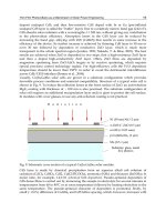
the H fields to be already normalized. Fig. 10(a,b) plots the band structure for
Δ=1.5( a/2),
h = 0.5a, d = 0.4a, and the values of for different branches of the dispersion curve. The
frequency scales are aligned along the y-axis so the value of the overlap is plotted along the
x-axis in Fig. 10b. The calculations indicate that the overlap between the bulk mode and the
mode from a waveguiding branch is indeed small (no greater than
∼ 2%). As expected, the
degree of the overlap within the other branch gradually increases away from the anti-
crossing. We argue that making the trench deeper (smaller d) and narrowing the width of
the trench (smaller
Δ) decreases the even- and odd- like character of the modes. The
reasoning is the following: by decreasing the depth of the waveguiding region, one is
introducing larger perturbations to the ideal, symmetric slab about z =0. Thus, the odd-like
and even-like modes interact to a greater extent, and the odd-even symmetry is lost. Further,
this should be seen in the overlap between the once even-like mode and the odd bulk mode.
If odd-even symmetry has decreased, then one expects the overlap to be greater. Indeed, the
calculations performed for a structure with
Δ = 1.25( a/2), h = 0.5a, d = 0.3a yield the
results qualitatively similar to those in Fig. 10, but with greater degree of the overlap.
Fig. 10. (a) Band structure diagram for h = 0.5a, d = 0.4a in the spectral vicinity of the region
of the strongest leakage of the guided mode (low dispersion curve). (b) plots (on the x-axis)
the overlap between the guided mode and the bulk mode of the opposite (odd) symmetry.
Dual-Periodic Photonic Crystal Structures
21
4.3 Control over the properties of the mode
4.3.1 The effect of trench depth
In Sec. 4.2.3 we have found that when the trench becomes too deep, the loss of the even
symmetry of the guided mode may lead to increased propagation losses. Here, we
investigate the possibility of tuning the optical properties of the trench waveguide while
keeping it shallow (h − d)
h.
We varied the parameter d between d = 0.36a and d = 0.46a in steps of d = 0.02a, while
Δ =
1.5 × (
a/2) and h = 0.5a were kept constant for all structures. The resulting dispersion
relations are plotted in Fig. 11. One observes that for lower values of d, the frequency of the
guided mode increases. This is to be expected, as the mode propagating in structures with a
deeper trench (smaller d) should have more spatial extent in regions of air. The associated
lowering of the effective index experienced by these modes leads to the increase of their
frequency
1
e
ff
n
ω
−
∝ .
Fig. 11. Dispersion relations for the guided mode in the trench PhCS waveguide with
parameters h = 0.5a,
Δ = 1.5( a/2), and different values of d. The even bulk PhCS modes
are superimposed as gray regions. A decrease in the depth of the trench (h − d) leads to the
decrease in the frequency of the guided mode in accordance with the effective index
argument, see text.
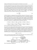
4.3.2 Trench displacement
One of the structural parameters important from the experimental point of view is the
alignment of the trench waveguide with the rows of cylindrical air-holes in the PhCS. To
demonstrate the robustness of the waveguiding effect in our design, we studied the
dependence of the band structure on the trench position. We introduce a displacement
parameter t
d
which measures the distance between the middle of the trench and the line
containing the centers of the air-holes. By our definition, the maximum amount of trench
displacement is t
d,max
= a × ( /4). By symmetry, any larger displacements are identical to
Recent Optical and Photonic Technologies
22
one in 0 ≤ t
d
≤ t
d,max
interval. The parameter t
d
was varied in this range in steps of t
d
=0.2×t
d,max
, while Δ = 1.5× ( a/2) and h = 0.5a were kept constant for all iterations. The
dispersion relation plots are presented in Fig. 12.
As t
d
approaches t
d,max
, we note that the frequency of the waveguiding band shifts only
slightly to lower frequencies. Thus, fabrication errors in the alignment of the trench with the
background photonic crystal slab should have minimal effects on the frequency of the band.
The most pronounced dependence on t
d
appears at the edge of the Brillouin zone, k = 1/2. At
t
d
= t
d,max
a degeneracy created between the guided mode and the next highest-frequency
even-like mode; the trench waveguide no longer operates in a single mode regime. This
degeneracy can be explained by studying the z-component of the magnetic field, H
z
. Fig. 12b
plots
ℜ[H
z
(x
0
,y, z)] for the guided mode with t
d
= 0 (upper panel) and t
d
= t
d,max
(lower panel).
x
0
corresponds to the line containing the centers of the airholes. At t
d,max
displacement, an
additional symmetry appears due to the fact that the trench is centered at the midpoint
between two consecutive rows of air-holes. As highlighted by the structure of the mode in
Fig. 12b, the combination of translation by a/2 along the direction of the trench (y-axis) and
the y − z mirror reflection leaves the structure invariant. Thus, the effective index sampled
by two modes related by the above symmetry transformation, is identical. For the k-vectors
other than 1/2, the two modes remain spectrally separated for a large range of t
d
, making
the system robust against misalignment errors during fabrication.
Fig. 12. Dispersion relations for h = 0.5a, d = 0.4a, and different values of the horizontal
position t
d
is shown in (a). The even bulk PhCS modes are superimposed as gray regions.
One notes that as t
d
approaches t
d,max
the bands become degenerate at the edge of the
Brillouin zone. Panel (b) depicts the guided mode with k = 1/2 for the trench centered at
(upper) or between (lower) rows of holes. Degeneracy of the lower mode for which t
d
= t
d,max
is explained by the added symmetry of the trench for this particular value of t
d
. This
symmetry involves a/2 translation and mirror reflection, see text.
Dual-Periodic Photonic Crystal Structures
23
4.4 Rotated trench waveguide as an array of coupled micro-cavities
As previously discussed in Sec. 4.1, a wide range of new phenomena is expected when the
direction of the trench waveguide is rotated with respect to the direction of the row of holes.
Indeed, a rotation of the trench creates modulations along the waveguide – the trench
alternates between the regions where it is centered on a hole and those between holes. We
will see that these regions play the role of optical resonators which are optically coupled (by
construction) to form a coupled resonator optical waveguide (CROW) (Yariv et al., 1999).
4.4.1 Effective index approximation analysis
In order to quantify the orientation of the trench, we use a parameter
α
, the angle between
the trench and the row of holes in the nearest neighbor direction. The investigation of such
structures can still be accomplished with the plane wave expansion method of Ref. (Johnson
& Joannopoulos, 2001). The required super-cell, however, is greatly increased (c.f. Fig. 15
below). To allow the detailed qualitative study of the rotated trench structures, we first
adopt an effective index approximation (Qiu, 2002), reducing the structures to two
dimensions. The slab is now a 2D hexagonal lattice with the background dielectric constant
ε = 12.0, with holes of radius r = 0.4a and ε
air
= 1.0. The trench is represented by a stripe
region with the reduced dielectric constant of ε = 3.0. A band gap is present in the spectrum
of the TE-polarization modes propagating though this structure, with the guided mode of
the same polarization. Similar to the original 3D system, the frequency of the mode is
displaced up into the band gap due to the linear defect. An example of the super-cell of the
2D dielectric structure being modeled is depicted in the inset of Fig. 13a.
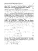
Fig. 13. (a) Band structure for the aligned trench waveguide
α
= 0˚ (solid line) is compared to
the extended Brillouin zone band structures of the rotated trench waveguides with
α
= 9.8˚
(squares),
α
= 7.1˚ (triangles), and
α
= 4.9˚ (diamonds). The slowest group velocity (flattest
band) occurs for the intermediate
α
= 7.1˚. The inset shows the 2D effective-medium
approximation of the 3D trench. (b) n(x
t
) as a function of trench coordinate x
t
. n(x
t
) is
modulated in a periodic fashion, allowing for the 1D photonic crystal methods to be applied.
We consider trenches with a small rotation from the M-crystallographic direction of the
hexagonal lattice. The smallness of the angle is determined in comparison to the other
nonequivalent direction, K, which is separated by an angle of 30˚. We studied the rotated
trench waveguides with several values of
α
; here we report the results on
α
= 9.8˚, 7.1˚ and
Recent Optical and Photonic Technologies
24
4.9˚. In order to model the structures with such small angles, a large (along the direction of
the waveguide) computational super-cell is needed. As the result, the band structure of
trench is folded due to reduction of the Brillouin zone (BZ)(Neff et al., 2007). Even when
unfolded, the size of the BZ is reduced because a single period along the direction of the
trench contains several lines of air-holes. Thus, to compare the dispersion of the rotated
waveguide to that of the straight one, in Fig. 13a we show their band structures in the
extended form. The obtained series of bands correspond to the different guided modes of
the trench waveguide. Strikingly, we observe that the group velocity v
g
= d
ω
(k)/dk
associated with different bands varies markedly, c.f. bands (a,b) indicated by the arrows in
Fig. 13a. The origin of such variations is discussed below.
4.4.2 Coupled resonator optical waveguide (CROW) description
As the trench defect crosses the lines of air-holes in the PhCS, the local effective index
experienced by the propagating mode varies, c.f. inset in Fig. 13a. This creates a one-
dimensional sequence of the periodically repeated segments with different modulations of
the refractive index. Indeed, Fig. 13b shows the refractive index averaged over the cross-
section of the trench and plotted along the waveguide direction. As it was shown Sec. 2, 3,
this dual-periodic (1D) photonic super-crystal acts as a periodic sequence of coupled optical
resonators. Furthermore, comparison of two modes in Fig. 14 demonstrates that at some
frequency, a segment of the trench may play the role of the cavity, whereas at another, this
particular section of the trench may serve as a tunneling barrier. This is similar to our results
in Fig. 1b.
For applications such as optical storage or coupled laser resonators, small-dispersion modes
(slow-light regime) are desired (Vlasov et al., 2005; Baba & Mori, 2007). Examining Fig. 13
we find that the band with the smallest group velocity (marked with (b) in the figure) occurs
at
α
= 7.1˚. Comparison of the fast (a) and slow (b) modes, c.f. Figs. 13a, 14, provides a clue
as to why there might exist such a dramatic variations in the dispersion. For mode (a) the
resonator portion of the trench is long, whereas the barrier separating two subsequent
resonator regions is short. The corresponding CROW mode is extended with weak
confinement and high degree of coupling between the resonators. For mode (b) the
resonator regions appear to be well separated, thus the cavities provide good confinement
while the coupling is quite weak. This results in low dispersion of the CROW band (b).
(a) (b)
Fig. 14. Spatial distribution of the wave-guidingmode, |H
z
|
2
, for the fast- and the slow-
bands denoted as (a) and (b) in Fig. 13a.
Dual-Periodic Photonic Crystal Structures
25
Our analysis of 1D structures in Ref. (Yamilov & Bertino, 2008) showed that increasing the
period of the super-modulation monotonously leads to flatter bands – simultaneously
enhancing confinement and weakening inter-cavity coupling. In the effective index
approximation of our trench waveguide, an increase of the super-modulation corresponds
to the decrease of the angle of rotation of the trench
α
. Lack of such a uniform reduction in
the group velocity of the guided modes with the decrease of
α
(in the system considered, the
minimum in v
g
occurs for the intermediate value of
α
= 7.1˚) shows that the reduction to 1D
system (such as in Fig. 13b) may not be fully justified. In other words, the position of the
trench with relation to the PhCS units is important in formation of the optical resonators,
hence, simulation of a particular structure in hand is required.
4.5 Implementation of trench-waveguide
Although the band structure computations become significantly more challenging when one
relaxes the effective index approximation employed in Sec. 4.4.1, 4.4.2, our CROW
description of the guided modes in the rotated trench waveguide remains valid. Fig. 15
shows a representative mode found in the full 3D simulations. In the realistic 3D systems
the CROW description is further complicated (Sanchis et al., 2005; Povinelli & Fan, 2006) due
to the need to account not only the in-plane confinement 1/Q
║
but also the vertical
confinement factor 1/Q
⊥
even in a single cavity (a single-period section of the trench).
Indeed, since the total cavity Q-factor contains both contributions 1/Q = 1/Q
║
+1/Q
⊥
, the
structures optimized in the 2D-approximation simulations which contain no Q
⊥
, no longer
appear optimized in 3D.
Fig. 15. A representative example of the guided mode obtained in full 3D simulation of the
rotated trench waveguide. The system parameters are chosen as in Sec. 4.3,
α
= 9.8˚.
Several designs aim at optimization of PhCS-based resonator cavities by balancing Q
║
and
Q
⊥
via “gentle localization” (Akahane et al., 2003), phase slip (Lončar et al., 2002; Apalkov &
Recent Optical and Photonic Technologies
26
Raikh, 2003) or double heterostructure (Song et al., 2005). In Ref. (Yamilov et al., 2006) we
also demonstrated how random fluctuation of the thickness of PhCS give rise to self-
optimization of the lasing modes. The results of Sec. 4.4.1, 4.4.2 suggest that by varying such
structural parameters of the trench waveguide as its width, depth and the rotation angle, a
variety of resonator cavities is created. Thus, we believe that, given a particular
experimental realization, it would be possible to optimize the guided modes of the trench
waveguide for the desired application. We stress that the adjustment of all three structural
parameters of the considered design does not require the alteration of the structural unit of
PhCS – the air-hole – and it should be possible to fabricate a trench waveguide in a PhCS
“blank” prepared e.g. holographically. Therefore, the fabrication process of the finished
device involving the trench waveguides may be accomplished without employing (serial)
e-beam lithography opening up a possibility of parallel mass production of such devices.
5. Summary and outlook
In this contribution we presented the analytical and numerical studies of photonic super-
crystals with short- and long-range harmonic modulations of the refractive index, c.f. Eq. (1).
Such structures can be prepared experimentally with holographic photolithography, Sec. 2.
We showed that a series of bands with anomalously small dispersion is formed in the
spectral region of the photonic bandgap of the underlying single-periodic crystal. The
related slow-light effect is attributed to the long-range modulations of the index, that leads
to formation of an array of evanescently-coupled high-Q cavities, Sec. 3.1.
In Sec. 3, the band structure of the photonic super-crystal is studied with four techniques: (i)
transfer matrix approach; (ii) an analysis of resonant coupling in the process of band folding;
(iii) effective medium approach based on coupled-mode theory; and (iv) the Bogolyubov-
Mitropolsky approach. The latter method, commonly used in the studies of nonlinear
oscillators, was employed to investigate the behavior of eigenfunction envelopes and the
band structure of the dual-periodic photonic lattice. We show that reliable results can be
obtained even in the case of large refractive index modulation.
In Sec. 4 we discussed a practical implementation of a dual-periodic photonic super-crystal.
We demonstrated that a linear trench defect in a photonic crystal slab creates a periodic
array of coupled photonic crystal slab cavities.
The main message of our work is that practical slow-light devices based on the coupled-cavity
microresonator arrays can be fabricated with a combination of scalable holography and photo-
lithography methods, avoiding laborious electron-beam lithography. The intrinsic feature
uniformity, crucial from the experimental point of view, should ensure that the resonances
of the individual cavities efficiently couple to form flat photonic band and, thus, bring about
the desired slow light effect. Furthermore, the reduction in fabrication costs associated with
abandoning e-beam lithography in favor of the optical patterning, is expected to make them
even more practical.
6. Acknowledgments
AY acknowledges support from Missouri University of Science & Technology. MH
acknowledges the support of a Missouri University of Science & Technology Opportunities
for Undergraduate Research Experiences (MST-OURE) scholarship and a Milton Chang
Travel Award from the Optical Society of America.
Dual-Periodic Photonic Crystal Structures
27
7. References
Akahane, Y., Asano, T., Song, B S., and Noda, S. (2003). “High-Q photonic nanocavity in a
two-dimensional photonic crystal,” Nature (London) 425, 944-947.
Altug, H., and Vučković, J. (2004). “Two-dimensional coupled photonic crystal resonator
arrays,” Appl. Phys. Lett. 84, 161.
Altug, H. & Vukovic, J. (2005). “Experimental demonstration of the slow group velocity of
light in two-dimensional coupled photonic crystal microcavity arrays,” Appl. Phys.
Lett. 86, 111102.
Apalkov, V. M., and Raikh, M. E. (2003). “Strongly localized mode at the intersection of the
phase slips in a photonic crystal without band gap,” Phys. Rev. Lett. 90, 253901.
Ashcroft, N. W., & Mermin, N. D. (1976). Solid State Physics, (Brooks Cole).
Baba, T., and Mori, D. (2007). “Slow light engineering in photonic crystals,” J. Phys. D 40,
2659-2665.
Bayindir, M., Tanriseven, S., and Ozbay, E. (2001). “Propagation of light through localized
coupled-cavity modes in one-dimensional photonic band-gap structures,” Appl.
Phys. A 72, 117-119.
Bayindir, M., Kural, C., and Ozbay, E. (2001). “Coupled optical microcavities in one-
dimensional photonic bandgap structures,” J. Opt. A 3, S184-S189.
Benedickson, J. M., Dowling, J. P., and Scalora, M. (1996). “Analytic expressions for the
electromagnetic mode density in finite, one-dimensional, photonic band-gap
structures,” Phys. Rev. E 53, 4107-4121.
Bertino, M. F., Gadipalli, R. R., Story, J. G., Williams, C. G., Zhang, G., Sotiriou-Leventis, C.,
Tokuhiro, A. T., Guha, S., and Leventis, N. (2004). “Laser writing of semiconductor
nanoparticles and quantum dots,” Appl. Phys. Lett. 85, 6007-6009.
Bertino, M. F., Gadipalli, R. R.,Martin, L. A., Rich, L. E., Yamilov, A., Heckman, B. R.,
Leventis, N., Guha, S., Katsoudas, J., Divan, R., and Mancini, D. C. (2007).
“Quantum dots by ultraviolet and X-ray lithography,” Nanotechnology 18, 315603.
Bogolyubov, N. N. & Mitropolsky, Yu. A. (1974). Asymptotic methods in theory of nonlinear
oscillations, (in Russian) (Moscow, Nauka).
Bristow, A. D., Whittaker, D. M., Astratov, V. N., Skolnick, M. S., Tahraoui, A., Krauss, T. F.,
Hopkinson, M., Croucher, M. P., and Gehring, G. A. (2003). “Defect states and
commensurability in dual-period AlxGa1-xAs photonic crystal waveguides,” Phys.
Rev. B 68, 033303.
Chutinan, A., and Noda, S. (2000). “Waveguides and waveguide bends in two-dimensional
photonic crystal slabs,” Phys. Rev. B 62, 4488-4492.
Cho, C. O., Jeong, J., Lee, J., Kim, I., Jang, D. H., Park, Y. S., and Woo, J. C. (2005). “Photonic
crystal band edge laser array with a holographically generated square-lattice
pattern,” Appl. Phys. Lett. 87, 161102.
Cho, C. O., Lee, J., Park, Y., Roh, Y G., Jeon, H., and Kim, I. (2007). “Photonic Crystal Cavity
Lasers Patterned by a Combination of Holography and Photolithography,” IEEE
Photonics Tech. Lett. 19, 556-558.
de Sterke, C. M. (1998). “Superstructure gratings in the tight-binding approximation,” Phys.
Rev. E 57, 3502-3509.
Dorado, L. A., Depine, R. A., and Miguez, H. (2007). “Effect of extinction on the high-energy
optical response of photonic crystals ,” Phys. Rev. B. 75, 241101.
Recent Optical and Photonic Technologies
28
Fleischer, J. W., Carmon, T., Segev, M., Efremidis, N. K., and Christodoulides, D. N. (2003).
“Observation of Discrete Solitons in Optically Induced Real Time Waveguide
Arrays,” Phys. Rev. Lett. 90, 023902.
Efremidis, N. K., Sears, S., Christodoulides, D. N., Fleischer, J. W., and Segev, M. (2002).
“Discrete solitons in photorefractive optically induced photonic lattices,” Phys.
Rev. E 66, 046602.
Galisteo-López, J. F. & López, C. (2004). “High-energy optical response of artificial opals,”
Phys. Rev. B 70, 035108.
Happ, T. D., Kamp, M., Forchel, A. Gentner, J L., and Goldstein, L. (2003). “Two-
dimensional photonic crystal coupled-defect laser diode,” Appl. Phys. Lett. 82, 4.
Herrera, M., and Yamilov, A. (2009). “Trench waveguide in photonic crystal slab
structures,” J. Opt. Soc. Am. B (submitted).
Hofstadter, D. R. (1976). “Energy levels and wave functions of Bloch electrons in rational
and irrational magnetic fields,” Phys. Rev. B 14, 2239.
Jacobsen, R. S., Andersen, K. N., Borel, P. I., Fage-Pedersen, J., Frandsen, L. H., Hansen, O.,
Kristensen, M., Lavrinenko, A. V., Moulin, G., Ou, H., Peucheret, C., Zsigri B., and
Bjarklev, A. (2006). “Strained silicon as a new electro-optic material,” Nature 441,
199-202.
Janner, D., Galzerano, G., Della Valle, G., Laporta, P., Longhi, S., and Belmonte, M. (2005).
“Slow light in periodic superstructure Bragg grating,” Phys. Rev. E 72, 056605.
Joannopoulos, J.D., Johnson, S. G., Winn, J.N., and Meade, R. D., (2008). Photonic Crystals:
Molding the Flow of Light, (2nd Ed., Princeton University Press, Princeton, NJ)
Johnson, S.G., Fan, S., Villeneuve, P.R., Joannopoulos, J.D., and Kolodziejski, L.A. (1999).
“Guided modes in photonic crystal slabs,” Phys. Rev. B 60, 5751-5758.
Johnson, S.G., Villeneuve, P.R., Fan, S., and Joannopoulos, J.D. (2000). “Linear waveguides
in photonic-crystal slabs,” Phys. Rev. B 62, 008212.
Johnson, S.G., and Joannopoulos, J.D. (2001). “Block-iterative frequency-domain methods for
Maxwell’s equations in a planewave basis,” Optics Express 8, 173-190.
Karle, T.J., Brown, D.H., Wilson, R., Steer, M., and Krauss, T.E. (2002). “Planar photonic
crystal coupled cavity waveguides,” IEEE J. of Selected Topics in Quantum Electr.,
8, 909 - 918.
Kitahara, H., Kawaguchi, T., Miyashita, J., Shimada, R., and Takeda, M. W. (2004). “Strongly
Localized Singular Bloch Modes Created in Dual-Periodic Microstrip Lines,” J.
Phys. Soc. Jap. 73, 296-299.
Krauss, T. F. (2003). “Planar photonic crystal waveguide devices for integrated optics,”
Phys. Stat. Sol. (a) 197, 688702.
Landa, P. S. (2001). Regular and Chaotic Oscillations, (Springer, Berlin).
Lifshitz, I. M., Gredeskul, S. A., and Pastur, L. A. (1988). Introduction to the Theory of
Disordered Systems, (Wiley, New York).
Liu, Z W., Du, Y., Liao, J., Zhu, S N., Zhu, Y Y., Qin, Y Q., Wang, H T., He, J L., Zhang,
C., and Ming, N B., (2002). “Engineering of a dual-periodic optical superlattice
used in a coupled optical parametric interaction,” J. Opt. Soc. Am. B 19, 1676-1684.
Lončar, M., Doll, T., Vuckovic, J., and Scherer, A. (2000). “Design and fabrication of silicon
photonic crystal optical waveguides,” J. of Lightwave Technology 18, 1402-1411.
Lončar, M., Yoshie, T., Scherer, A., Gogna, P., and Qiu, Y. (2002). “Low-threshold photonic
crystal laser,” Appl. Phys. Lett. 81, 2680.
Dual-Periodic Photonic Crystal Structures
29
Marcuse, D. (1991). Theory of Dielectric Optical Waveguides, 2nd ed. (Academic, San Diego).
Milonni, P. W. (2005). Fast light, slow light and left-handed light, (Institute of Physics, Bristol).
Neff, C. W., Yamashita, T., and Summers, C. J. (2007). “Observation of Brillouin zone folding
in photonic crystal slab waveguides possessing a superlattice pattern,” Appl. Phys.
Lett. 90, 021102.
Neshev, D., Ostrovskaya, E., Kivshar, Y., and Krolikovwski, W. (2003). “Spatial solitons in
optically induced gratings,” Opt. Lett. 28, 710-712.
Nojima, S. (1998). “Enhancement of optical gain in two-dimensional photonic crystals with
active lattice points,” Jpn. J. Appl. Phys. Part 2 37, L565-L567.
Olivier, S., Smith, C., Rattier, M., Benisty, H., Weisbuch, C., Krauss, T., Houdr´e, R., and
Oesterl´e, U. (2001). “Miniband transmission in a photonic crystal coupled-
resonator optical waveguide,” Opt. Lett. 26, 1019-1021.
Painter, O., Lee, R. K., Scherer, A., Yariv, A., O’Brien, J. D., Dapkus, P. D., and Kim, I. (1999).
“Two-Dimensional Photonic Band-Gap Defect Mode Laser,” Science 284, 1819.
Park, H., Kim, S., Kwon, S., Ju, Y., Yang, J., Baek, J., Kim, S., and Lee, Y. (2004). “Electrically
Driven Single-Cell Photonic Crystal Laser,” Science 305, 1444.
Poon, J. K. S., Scheuer, J., Xu, Y., and Yariv, A. (2004). “Designing coupled-resonator optical
waveguide delay lines,” J. Opt. Soc. Am. B 21, 1665-1673.
Poon, J. K. S., Zhu, L., DeRose, G. A., and Yariv, A. (2006). “Polymer Microring Coupled-
Resonator Optical Waveguides,” J. Lightwave Technol. 24, 1843-1849.
Povinelli, M. L. and Fan, S. (2006). “Radiation loss of coupled-resonator waveguides in
photonic-crystal slabs,” Appl. Phys. Lett. 89, 191114.
Qiu, M. (2002). “Effective index method for heterostructure-slab-waveguide-based
twodimensional photonic crystals,” Appl. Phys. Lett. 81, 1163.
Sakoda, K. (1999). “Enhanced light amplification due to group-velocity anomaly peculiar to
two- and three-dimensional photonic crystals,” Opt. Express 4, 167-176.
Sanchis, P., Marti, J., Bogaerts, W., Dumon, P., Van Thourhout, D., and Baets, R. (2005).
“Experimental results on adiabatic coupling into SOI photonic Crystal coupled-
cavity waveguides,” IEEE Photonics Tech. Lett. 17, 1199 - 1201.
Scharrer, M., Yamilov, A., Wu, X., Cao, H., and Chang, R. P. H. (2006). “Ultraviolet lasing in
high-order bands of three-dimensional ZnO photonic crystals,” Appl. Phys. Lett.
88, 201103.
Scheuer, J., Paloczi, G., Poon, J., and Yariv, A. (2005). “Toward the Slowing and Storage of
Light,” Opt. and Phot. News 16, 36.
Shimada, R., Koda, T., Ueta, T., and Ohtaka, K. (1998). “Energy Spectra in Dual-Periodic
Multilayer Structures,” J. Phys. Soc. Jap. 67, 3414-3419.
Shimada, R., Koda, T., Ueta, T., and Ohtaka, K. (2001). “Strong localization of Bloch photons
in dual-periodic dielectric multilayer structures,” J. Appl. Phys. 90, 3905-3909.
Sipe, J. E., Poladian, L., and de Sterke, C. M. (1994). “Propagation through noniniform
grating structures,” J. Opt. Soc. Am. A 11, 1307-1320.
Soljacic, M., Johnson, S. G., Fan, S., Ibanescu, M., Ippen, E., and Joannopoulos, J. D. (2002).
“Photonic-crystal slow-light enhancement of nonlinear phase sensitivity,” J. Opt.
Soc. Am. B 19, 2052-2059.
Song, B S., Noda, S., Asano, T., and Akahane, Y. (2005). “Ultra-high-Q photonic double-
heterostructure nanocavity,” Nat. Mater. 4, 207-210.
Soukoulis, C. M., ed. (1996). Photonic band gap materials, (Kluwer, Dordrecht).
Recent Optical and Photonic Technologies
30
Stefanou, N. & Modinos, A. (1998). “Impurity bands in photonic insulators,” Phys. Rev. B
57, 12127-12133.
Susa, N. (2001). “Threshold gain and gain-enhancement due to distributed-feedback in two-
dimensional photonic-crystal lasers,” J. Appl. Phys. 89, 815-823.
Vlasov, Y. A., Moll, N., and McNab, S. J. (2004). “Mode mixing in asymmetric double-trench
photonic crystal waveguides,” J. Appl. Phys. 95, 4538-4544.
Vlasov, Yu. A., O’Boyle, M., Hamann H. F., and McNab, S. J. (2005). “Active control of slow
light on a chip with photonic crystal waveguides,” Nature 438, 65-69.
Xu, Y., Lee, R. K., and Yariv, A., (2000). “Propagation and second-harmonic generation of
electromagnetic waves in a coupled-resonator optical waveguide,” J. Opt. Soc. Am.
B 17, 387-400.
Yablonovitch, E. (1987). “Inhibited Spontaneous Emission in Solid-State Physics and
Electronics,” Phys. Rev. Lett. 58, 2059-2062.
Yagasaki, K., Merhasin, I.M., Malomed, B. A.,Wagenknecht, T., and Champneys, A. R.
(2006). “Gap solitons in Bragg gratings with a harmonic superlattice,” Europhys.
Lett. 74, 1006-1012.
Yamilov, A., Wu, X., Liu, X., Chang, R. P. H., and Cao, H. (2006). “Self-optimization of
optical confinement in ultra-violet photonic crystal slab laser,” Phys. Rev. Lett. 96,
083905.
Yamilov A., & Bertino, M. (2007). “Disorder-immune coupled resonator optical waveguide,”
Opt. Lett. 32, 283-285.
Yamilov, A., Herrera, M. R., and Bertino, M. F. (2008). “Slow light effect in dual-periodic
photonic lattice,” J. Opt. Soc. Am. B 25, 599-608.
Yanik, M. F., and Fan, S. (2004). “Stopping Light All Optically,” Phys. Rev. Lett. 92, 083901.
Yariv, A., Xu, Y., Lee, R. K., and Scherer, A. (1999). “Coupled-resonator optical waveguide: a
proposal and analysis,” Opt. Lett. 24, 711-713.
Yeh, P. (2005). “Optical waves in layered media,” (Wiley, Hoboken).
2
Two-Dimensional Photonic Crystal Micro-
cavities for Chip-scale Laser Applications
Adam Mock
1
and Ling Lu
2
1
Central Michigan University
2
University of Southern California
USA
1. Introduction
1.1 Photonic crystals
In this chapter we will focus on two-dimensional photonic crystal devices and emphasize
their use as building blocks in photonic integrated circuits with applications in high
bandwidth optical communication systems. In particular we will discuss recent progress in
designing high quality (Q) factor resonant cavities for building efficient micro- and nano-
cavity lasers. The first section will provide a brief overview of two-dimensional photonic
crystals and motivate their use in photonic integrated circuits. This will be followed by a
first principles derivation of the role of the Q factor in estimating laser threshold. We will
then focus on the photonic crystal heterostructure cavity due to its exceptionally large Q
factor. Its spectral and modal properties will be discussed, and its use as a high output
power edge-emitting laser will be presented. We conclude with remarks on continuous
wave laser operation via heat sinking lower substrates and the issue of out-of-plane loss.
The term photonic crystal refers to any structure with a periodic variation in its refractive
index (John, 1987; Yablonovitch et al., 1991; Joannopoulos et al., 1995). The periodicity can be
in one, two or three spatial dimensions and can introduce a photonic bandgap (a range of
frequencies for which electromagnetic radiation is non-propagating) with the same
dimensionality. The bandgap arises due to Bragg reflection and occurs when the spatial
periodicity has a length scale approximately one half that of the incident electromagnetic
radiation. This same phenomenon gives rise to the electronic bandgap in semiconducting
materials. Examples of photonic crystal structures with periodicity in varying spatial
dimensions are shown in Figure 1. One dimensional photonic crystals have found many
technology applications in the form of Bragg reflectors which are part of the optical
feedback mechanism in distributed feedback lasers (Kogelnik & Shank, 1971; Nakamura et
al., 1973) and vertical cavity surface emitting lasers (Soda et al., 1979). Two and three
dimensional photonic crystals have been the subject of intense research recently in areas
related to sensing (Lončar et al., 2003; Chow et al., 2004; Smith et al., 2007),
telecommunications (Noda et al., 2000; McNab et al., 2003; Bogaerts et al., 2004; Notomi et
al., 2004; Noda et al., 2000; Jiang et al., 2005; Aoki et al., 2008), slow light (Vlasov et al., 2005;
Krauss, 2007; Baba & Mori, 2007; Baba, 2008) and quantum optics (Yoshie et al., 2004; Lodahl
et al., 2004; Englund et al., 2005).
Recent Optical and Photonic Technologies
32
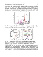
Fig. 1. Images depicting photonic crystals with periodicity in (a) one dimension, (b) two
dimensions and (c) three dimensions.
Figure 1(b) displays a semiconductor slab perforated with a two-dimensional triangular
array of air holes. Because of the periodic refractive index, the in-plane propagating modes
of the slab can be characterized using Bloch’s theorem. In the vertical, out-of-plane direction,
the modes are confined via index guiding, and Figure 2(a) illustrates typical guided and
radiation modes. These modes are peaked near the center of the slab and are either
evanescent (guided) or propagating (radiation) out-of-plane. Figure 2(b) is a photonic band
diagram corresponding to a photonic crystal structure similar to that shown in Figure 1(b)
and Figure 2(a). The left vertical axis is written in terms of normalized frequency where a
corresponds to the lattice constant of the photonic crystal, and c is the vacuum speed of
light. The right vertical axis is denormalized and written in terms of free space wavelength
using a lattice constant of a = 400nm. The photonic bandgap corresponds to the normalized
frequency range 0.25-0.32 where there are no propagating modes in this structure. Using a
lattice constant of a = 400nm places the near infrared fiber optic communication
wavelengths of 1.3μm (low-dispersion) and 1.5μm (low-loss) within the bandgap making
this geometry amenable to applications in fiber optic communication systems. The shaded
regions on the left and right sides of Figure 2(b) represent the projection of the light cone
onto the various propagation directions which is a result of the vertical confinement
mechanism being due to index guiding. Photonic crystal modes that overlap the shaded
regions in Figure 2(b) correspond to the radiation modes in Figure 2(a). Figure 2(b) shows
the dispersion for the three lowest frequency bands with transverse electric polarization
(out-of-plane magnetic field has even vertical symmetry). Figure 2(c) illustrates a unit cell
corresponding to a triangular lattice photonic crystal. The band diagram in Figure 2(b) was
calculated using the three-dimensional finite-difference time-domain method (Taflove &
Hagness, 2000). The computational domain is similar to that shown in Figure 2(c) where the
in-plane boundaries are terminated using Bloch boundary conditions. More details about
this approach can be found in (Kuang et al., 2007). Photonic crystal geometries represent
complicated electromagnetic problems and almost always demand a numerical approach
for their analysis. Several numerical methods for solving Maxwell’s equations exist. Some
examples include the finite-element method (Kim 2004), transmission line method (Benson
et al., 2005), scatterning based methods (Peterson et al., 1998; Sadiku 2000) and plane wave
expansion methods for periodic structures (Joannopoulos et al., 1995; Sakoda 2001). In this
work, we will be using the finite-difference time-domain method due to its generality,
simplicity and linear scaling with problem size. For the band structure in Figure 2(b), the
refractive index of the slab was set to n = 3.4, the hole radius to lattice constant ratio was set
Two-Dimensional Photonic Crystal Micro-cavities for Chip-scale Laser Applications
33
to r/a = 0.29 and the slab thickness to lattice constant ratio was set to d/a = 0.6. These
photonic crystal geometry parameters will hold for the rest of the devices analyzed in this
chapter.
Fig. 2. (a) Cross section of a two-dimensional photonic crystal defined in a dielectric slab of
finite thickness. The field distribution in the vertical direction for guided and radiation
modes is shown. (b) Photonic band diagram for a two-dimensional photonic crystal defined
in a single-mode slab. c denotes free space speed of light. a denotes the lattice cosntant. The
diagram depicts the lowest three bands for the TE-like modes of the slab. The inset shows
the region of the first Brillouin zone described by the dispersion diagram. (c) A unit cell of a
triangular photonic crystal lattice and the phase relationships between the boundaries
determined by Bloch’s theorem.
1.2 Defects in two-dimensional photonic crystals
Much of the versatility and device applications of two-dimensional photonic crystal
structures are associated with the introduction of defects into the periodic lattice. Figure 3(a)
displays the out-of-plane component of the magnetic field of a typical mode associated with
a photonic crystal waveguide formed by removing a single row of holes along the Γ − K
direction. For the TE-like modes of the slab, only the E
x
, E
y
and H
z
fields are nonzero at the
midplane, and H
z
is displayed due to its scalar nature. It is clear that the mode is localized to
the defect region along the y-direction due to the photonic crystal bandgap, and
confinement along the z-direction is due to index guiding as discussed with regard to Figure
2(a). Figure 3(b) displays the unit cell used in the computation of the field shown in Figure
3(a). The finite-difference time-domain method was used with Bloch boundary conditions
along the x-direction (Kuang et al., 2006). Figures 6(b) and 7 depict photonic crystal
waveguide dispersion diagrams. The mode depicted in Figure 3(a) is associated with the
lowest frequency band in the bandgap and a propagation constant of βa = 1.9. It has been
shown that photonic crystal waveguides are capable of low loss optical guiding (McNab et
al., 2003) and have the ability to redirect light along different directions in-plane with low
loss waveguide bends (Shih et al., 2004).
Figure 3(c) displays the z-component of the magnetic field corresponding to a typical
resonant mode of an L3 cavity (Akahane et al., 2003, 2005). The L3 cavity is formed by
removing three adjacent holes along the Γ − K direction in a triangular photonic crystal
lattice. The two dimensional in-plane confinement due to the photonic crystal bandgap is
apparent. In the case of photonic crystal defect cavities, a single unit cell with Bloch
boundary conditions is no longer applicable, and large three dimensional computational
domains must be analyzed. Such a cavity can be used as an optical filter, an optical buffer or
a laser.
Recent Optical and Photonic Technologies
34
Fig. 3. (a) H
z
(x,y, z = 0) for a typical photonic crystal waveguide mode. z = 0 corresponds to
the midplane of the slab as shown in Figure 2(a). (b) The unit cell of a photonic crystal
waveguide and the phase relationship between the boundaries determined by Bloch’s
theorem. (c) H
z
(x,y, z = 0) for a typical L3 cavity mode.
1.3 Photonic integrated circuits
Photonic integratration is analogous to the integration of electronic devices on a silicon chip.
Typical microprocessors contain on the order of 10
9
transistors in an area on the order of
1cm
2
. Such dense device integration has resulted in microprocessors with exceptional
functionality. And because the devices share a common substrate and metal wiring network,
they can be mass produced with limited overhead costs.
Similar to electronic integrated circuits, photonic integrated circuits are useful for any
application in which a large number of devices need to be contained in a confined space.
Photonic integrated circuits have a variety of applications including telecommunications,
sensing and imaging. In telecommunication systems photonic integrated circuits have the
potential for lower cost systems due to reduced packaging costs, improved reliability due to
reduced alignment errors and improved bandwidth through all optical signal processing.
Another application of photonic integrated circuits is in optical buses in multicore computer
architectures. The inter-core communication and off-chip memory access can be a
performance bottleneck for applications with heavy memory access. Optics has the potential
to improve memory access bandwidth due in part to its ability to transmit signals at
multiple wavelengths through a single waveguide. It also has the advantage of operating at
a lower temperature due to the absence of resistive heating.
Figure 4 shows a schematic diagram of a photonic crystal based photonic integrated circuit
that includes sources, modulators, filters and detectors integrated on a single chip. This
particular structure consists of a bus waveguide passing from left to right carrying
modulated optical signals at wavelengths λ
1
and λ
2
. First, the signals encounter frequency
selective filters which couple the filtered signal to an optical detector. On-chip lasers
operating at λ
1
and λ
2
generate a new carrier beam which is modulated and rerouted to the
bus waveguide. The input and output ports could lead to other on-chip processing or to
coupled optical fibers. From this simple example, it is clear that photonic crystals offer a
versatile platform for realizing a variety of different devices by local rearrangements of the
Two-Dimensional Photonic Crystal Micro-cavities for Chip-scale Laser Applications
35
Fig. 4. Schematic diagram depicting a simple photonic crystal based photonic integrated
circuit.
hole pattern. It is this flexibility along with their dispersive properties and high Q factor
cavities that make photonic crystals an interesting candidate for photonic integration.
Furthermore, devices based on photonic crystals have the potential to occupy smaller spaces
than devices based on index guiding. In the remainder of this chapter we will focus our
attention to aspects of designing photonic crystal cavities for on-chip laser sources.
2. High quality factor photonic crystal cavities
2.1 Role of the quality factor in determining laser threshold
The Q factor is a figure of merit used to quantify the radiation losses of an optical resonator.
Formally it is defined by
0
=.
U
Q
dU
dt
ω
〈
〉
−
〈〉
(1)
where ω
0
is the resonance frequency, and the angled brackets denote a time-average over an
integer number of optical periods. U represents the electromagnetic energy and is given by
1
=[
2
U
∫
ε
1
].
2
EE HHdV
μ
⋅+ ⋅
G
GGG
(2)
where ε represents the electric permittivity,
E
G
represents the electric field, μ represents the
magnetic permeability and
H
G
represents the magnetic field. Equation 1 can be considered a
first order ordinary differential equation in 〈U〉. Its solution is
0
() = (0) exp( / ).Ut U t Q
ω
〈
〉〈 〉 − (3)
Recent Optical and Photonic Technologies
36
Equation 3 tells us that the temporal decay of the electromagnetic energy stored in a large Q
factor cavity will be slower than that of a low Q factor cavity. From Eq. 3 a photon lifetime
can be defined as τ
p
= Q/ω
0
. This quantity is related to the average length of time that a
photon spends inside a cavity. It is clear that a large Q factor results in a long photon
lifetime.
In order to illustrate the precise role that the Q factor plays in designing efficient, low-
threshold lasers, we will derive the laser threshold condition applicable to photonic crystal
resonant cavities made from semiconductor active material (Mock & O’Brien, 2009a).
Equation 4 is the Poynting theorem in its time averaged form and is a statement of
electromagnetic energy conservation.
S
G
is the Poynting vector and is given by
=SEH×
G
GG
.
Its closed surface integral represents the power radiated through the surface. P
a
represents
absorbed power which in the case of a semiconductor active material would occur in regions
of the structure in which the carrier population is not inverted. P
s
represents supplied power
coming in the form of optical gain resulting from an external energy source.
=
as
U
SdA P P
t
∂
〈
〉⋅ −〈 〉−〈 〉+〈 〉
∂
∫
G
G
v
(4)
If one considers a passive cavity in which P
s
= P
a
= 0 and substitutes dU/dt in Equation 1 into
Equation 4 one gets
0
=.
m
m
p
U
SdA
Q
ω
〈
〉
〈〉⋅
∫
G
G
v
(5)
where the subscript m is used to specify that the Poynting vector and electromagnetic
energy correspond to a specific mode m whose passive Q factor is given by Q
p
. The basic
idea behind laser threshold is that the optical loss mechanisms should be exactly
compensated by an optical power source which comes in the form of optical gain (Schawlow
& Townes, 1958). At threshold when the loss just equals the gain, the temporal rate of
change of the energy in the cavity is zero, and we can set dU/dt = 0 in Equation 4. If we then
use Equation 5 in Equation 4, the result is
0
=.
m
as
p
U
PP
Q
ω
〈〉
+
〈〉 〈〉 (6)
Equation 6 is the laser threshold condition. The first term on the left side represents passive
cavity (radiative) losses. The second term represents active cavity (absorptive) losses. The
right side represents the supplied power required to offset the optical losses. From the first
term in Equation 6, it is apparent that the passive Q factor should be as large as possible so
as to reduce the radiative losses and thus the power required to reach threshold. It should be
noted, however, that a high Q factor cavity often results in reduced output power, and
tradeoffs between low threshold and sufficient output power should be considered when
designing a prospective cavity for chip-scale laser applications.
2.2 Two-dimensional photonic crystal cavities
Figure 5 displays four cavity designs as well as the evolution of their Q factors over the
passed decade. Early photonic crystal cavities were formed by removing a single hole from
Two-Dimensional Photonic Crystal Micro-cavities for Chip-scale Laser Applications
37
a uniform lattice (Painter et al., 1999; Ryu et al., 2002). More recently, linear defects have
been shown to have higher Q factors than single missing hole cavities (Akahane et al., 2003,
2005), and the photonic crystal double heterostructure cavity has been shown to have the
largest Q factor among two-dimensional photonic crystal cavities (Song et al., 2005; Tanaka
et al., 2008). Because of its exceptionally high Q factor and small mode volume, the photonic
crystal double heterostructure has been the subject of intense research for building efficient
chip scale optical sources and will be highlighted in what follows.
Fig. 5. Quality factor for different two-dimensional photonic crystal cavities as a function of
time. Data points and figures come from (Painter et al., 1999; Ryu et al., 2002; Akahane et al.,
2003; Zhang & Qiu, 2004; Nozaki & Baba, 2006; Akahane et al., 2005; Song et al., 2005; Asano
et al., 2006; Tanaka et al., 2008)
3. Photonic crystal double heterostructure resonant cavities
3.1 Introduction
In 2005 Song et al. showed that a two-dimensional photonic crystal waveguide with a small,
localized perturbation can form an ultra high Q factor cavity with a Q factor greater than 10
5
and a mode volume on the order of one cubic wavelength (Song et al., 2005, 2007). Such a
cavity was termed a photonic crystal double heterostructure and is depicted in Figure 6. The
cavity is formed from an otherwise uniform photonic crystal waveguide by enlarging the
lattice constant along the x-direction of the light colored air holes. Below the schematic
diagram, the resulting photonic band structure is shown illustrating the formation of a
photonic well along the x-direction. Further experimental work on these cavities has
Recent Optical and Photonic Technologies
38
demonstrated devices with passive Q factors as large as 10
6
(Asano et al., 2006). Since these
initial reports, several groups have reported forming high Q factor photonic crystal double
heterostructure cavities through a variety of methods including local modulation of a
photonic crystal line defect width (Kuramochi et al., 2006), local air-hole infiltration (Smith
et al., 2007), photosensitive materials (Tomljenovic-Hanic et al., 2007), effective index change
through micro-fiber coupling (Kim et al., 2007) and local modulation of the hole radii (Kwon
et al., 2008b). A numerical analysis showed that Q factors as high as 10
9
are possible with a
tapered perturbation (Tanaka et al., 2008). The ultra high Q factors and cubic wavelength
mode volumes along with the waveguide-like shape of the cavities have made them
attractive for a variety of applications including chemical sensing (Kwon et al., 2008a), slow
light (Tanabe et al., 2007; Takahashi et al., 2007), elements of coupled resonator optical
waveguides (O’Brien et al., 2007) and edge-emitting lasers (Shih, Kuang, Mock, Bagheri,
Hwang, O’Brien & Dapkus, 2006; Shih, Mock, Hwang, Kuang, O’Brien & Dapkus, 2006;
Yang et al., 2007; Lu et al., 2007, 2008; Lu, Mock, Shih, Hwang, Bagheri, Stapleton, Farrell,
O’Brien & Dapkus, 2009).
Fig. 6. (a) Schematic diagram of a photonic crystal double heterostructure resonant cavity
formed in a uniform single line defect waveguide by increasing the lattice constant of the
light colored holes along the x-direction. The resulting photonic well diagram is illustrated
below. (b) Photonic crystal waveguide dispersion diagram depicting the photonic crystal
waveguide bands associated with the straight (black, solid) and perturbed (red, dashed)
portions of the waveguide. The waveguide frequencies of the perturbed section that fall into
the mode gap of the straight waveguide are labeled “candidate bound state frequencies.”
The blue region denotes the photonic crystal cladding modes, and the gray region denotes
the light cone.
3.2 Spectral and modal properties
When the lattice constant is locally increased, it shifts the frequencies of the waveguide band
associated with the perturbed region to lower frequencies as shown in Figure 6(b). The
bound state will oscillate near frequencies of the perturbed waveguide section that fall into
the mode gap of the uniform waveguide sections. Candidate frequencies for bound state
resonances are labeled in Figure 6(b). Only below the minima of the dispersion relation in
Two-Dimensional Photonic Crystal Micro-cavities for Chip-scale Laser Applications
39
the uniform photonic crystal waveguide regions is there a possibility for a mode to exist in
the central region without the possibility of there simultaneously being a mode in the
cladding at the same frequency a small distance in wavevector away. In other words, only in
these cases is there no mode that is nearby (in the wavevector sense) in the cladding at the
same frequency (Mock et al., 2006, 2008). This mode formation is analogous to the formation
of bound states in electronic heterostructures at the extrema of the electronic dispersion
relations.
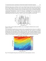
Figure 7 is a comparison between the spectral features of a photonic crystal double
heterostructure resonance spectrum and the frequency axis of the photonic crystal
waveguide dispersion diagram corresponding to the underlying straight waveguide. The
red dotted lines illustrate that the bound state resonance frequencies occur just below the
waveguide dispersion minima. The resonance spectrum was obtained by taking a discrete
Frourier transformation of a 2×10
5
element time sequence. The time sequence was calculated
via the three dimensional finite-difference time-domain method. The computational domain
included 20 uniform photonic crystal cladding periods on either side of the central defect
region along the x-direction and 8 photonic crystal layers above and below the central
waveguide core along the y-direction. This geometry was discretized with 950 × 340 × 200
discretization points along the x × y × z directions and parallelized using 11 × 4 × 3
processors (132 total processors) along the x × y × z directions. The geometry was discretized
using 20 points per lattice constant (a). The lattice constant of the perturbed region was
increased by 5% along the x-direction.
Fig. 7. Left: photonic crystal waveguide dispersion diagram. Black lines correspond to the
photonic crystal waveguide dispersion bands. Blue regions denote photonic crystal cladding
modes. The gray region denotes the light cone projection. Right: photonic crystal double
heterostructure resonant spectrum. Dashed lines illustrate correspondance between
heterostructure bound state frequencies and waveguide dispersion extrema.
Figure 8 depicts the z-component of the magnetic field for the bound state resonances
labeled in Figure 7. These mode profiles may be interpreted as consisting of the waveguide
mode of the underlying straight waveguide multiplied by a confining envelope function
centered at the perturbation. It is interesting to point out that mode (c) exhibits significant
Recent Optical and Photonic Technologies
40
extension into the photonic crystal cladding. This can be attributed to the close proximity of
the corresponding photonic crystal waveguide band to the photonic crystal cladding modes
in Figure 7. To the right of each H
z
(x,y, z = 0) mode profile is the corresponding spatial
Fourier transform. Specifically, log(|FT(E
x
)|
2
+ |FT(E
y
)|
2
) is plotted where FT stands for
Fourier transform. The two-dimensional spatial Fourier transform yields the spatial
wavevector components that make up the bound state resonance. The spatial wavevector
distributions are centered at β
x
= ±π/a. This is consistent with the observation that bound
state resonance frequencies occur near the waveguide dispersion minima which coincide
with the Brillouin zone boundary at β
x
= ±π/a for this particular waveguide.
Fig. 8. Left: H
z
(x, y, z = 0) for the three modes summarized in Table 1. Right: spatial Fourier
transform log(|FT(E
x
)|
2
+ |FT(E
y
)|
2
) of each mode illustrating the distribution of spatial
wavevectors making up the different resonant modes.
Table 1 summarizes the normalized resonance frequencies of the three modes shown in
Figure 8. The resonance frequencies and Q factors were obtained using the Padé
interpolation method (Mock & O’Brien, 2008). It is clear that the bound state resonance
Two-Dimensional Photonic Crystal Micro-cavities for Chip-scale Laser Applications
41
frequencies fall just below the photonic crystal waveguide band edge. Mode (a) has the
largest Q factor and will be featured in the remainder of this chapter.
Mode
Resonance
Frequency
Bandedge
Frequency
Q factor
(a) 0.2606 0.2629 336,700
(b) 0.2800 0.2824 10,800
(c) 0.3184 0.3227 8,250
Table 1. Summary of Q factors and resonant frequencies for the resonant modes associated
with a photonic crystal heterostructure cavity.
3.3 Higher-order bound states
The previous section discussed a photonic crystal double heterostructure cavity resulting
from a 5% lattice constant stretching along the x-direction. Figure 9 shows several
interesting features of the high Q factor mode in Table 1 as the degree of perturbation is
varied. First, the Q factor exhibits a strong dependence on the percent lattice constant
increase. For very shallow perturbations (<3%), Q factors in excess of one million are
predicted. Whereas for perturbations exceeding 20%, the Q factor dips below one thousand.
Intuitively, one would expect that by increasing the lattice constant perturbation, the
photonic well is deepened which would lead to improved confinement. It turns out that
deepening the well makes the transition between the straight waveguide and the
perturbation region more abrupt and introduces high spatial frequencies into the envelope
function of the mode along the x-direction (Akahane et al., 2003). Because these modes have
Fourier space distributions centered near β
x
= π/a, large spatial frequencies in the envelope
function get shifted to regions in Fourier space near β
x
=0. Fourier components inside the
light cone centered at the origin in Fourier space radiate out-of-plane, and this loss
mechanism dominates the overall loss properties of the mode. Researchers have
investigated designs that smoothen the transition between the straight waveguide regions
and the perturbation region and have obtained improved Q factors as a result (Akahane et
al., 2005; Song et al., 2005).
Fig. 9. Q factor versus perturbation depth for the first, second and third order bound states.
Recent Optical and Photonic Technologies
42
The second interesting feature of Figure 9 is the presence of higher order bound states. For
perturbations greater than 7.5%, the cavity supports both a first order and a second order
bound state. For perturbations greater than 20%, the cavity supports three bound states. The
Q factors of the higher order bound state resonances exhibit a similar dependence on
percent lattice constant increase as the first order bound state. It should also be pointed out
that for a given perturbation, the highest order bound state has the largest Q factor. Figure
10 displays the z-component of the magnetic field of the first three bound states associated
with a heterostructure cavity. Also shown are the envelope functions obtained by extracting
Fig. 10. Left: H
z
(x, y, z = 0) field distributions for the first, second and third order bound
states. Right: field envelopes extracted from |H
z
(x, y = 0, z = 0)|.
Two-Dimensional Photonic Crystal Micro-cavities for Chip-scale Laser Applications
43
the maxima of |H
z
(x,y = 0, z = 0)| (the dotted white line in the top image of Figure 10
depicts the contour along which the maxima were measured). The envelope functions show
a similar behavior to the wavefunction solutions corresponding to a quantum well problem
in quantum mechanics.
From a technology perspective, if one chooses to work with a cavity that supports multiple
bound states, then it is useful to be able to enhance one mode relative to the others. From
Equation 6, one sees that the mode with the largest Q factor will be the first to reach threshold
if the cavity is multimoded. However, from Figure 10, the various bound states have different
spatial mode distributions and thus different overlap integrals with the spatial gain
distribution. For instance, an optical pump beam directly centered on the heterostructure
cavity will preferentially pump the first order bound state, and this mode could reach
threshold first even though it has a smaller Q factor than the second order bound state. In
order to get around this issue one can introduce cavity modifications that significantly reduce
the Q factors of the unwanted modes while leaving the Q factor of the featured mode intact.
Such a mode discrimination scheme improves side mode suppression as well.
One strategy to perform mode discrimination is to place extra holes in the cavity near the
maxima of the electric field corresponding to the mode we wish to suppress. This enhances
out-of-plane radiation and lowers the Q factor (Kuang et al., 2005). Figure 11 displays
modified cavities that were fabricated in a 240-nm-thick suspended InGaAsP membrane
containing four compressively strained quantum wells. The semiconductor dry-etch was
done in an inductively coupled plasma etcher using BCl
3
chemistry at 165°C. The rest of the
fabrication processes are the same as those in (Shih, Kuang, Mock, Bagheri, Hwang, O’Brien
& Dapkus, 2006). The inset of Figure 11(a) displays a scanning electron micrograph of a
cavity with a 10% perturbation which supports both the first order and the second order
bound states. The inset of Figure 11(b) illustrates a cavity with holes placed at x = ±2.4a to
suppress the second order bound state, and Figure 11(c) illustrates a cavity with a hole
placed at x = 0 to suppress the first order bound state (Mock et al., 2009).
The devices were optically pumped at room temperature by an 850 nm diode laser at
normal incidence with an 8 ns pulse width and 1% duty cycle. The size of the pump spot
was about 2 μm in diameter. The lower spectrum in Figure 11(a) is the single-mode lasing
spectrum operating in the first bound state, while the upper multimode lasing spectrum
shows the existence of the second bound state approximately 20 nm away from the first one
when the pump spot is slightly moved off the device center along the waveguide core. The
two modified structures in Figure 11(b) and (c) both operate in stable single-mode operation
with respect to pump beam location. Their lasing wavelengths line up with the first and
second bound states lasing in the unmodied structure. All four lasing spectra were taken at
the peak incident power of 1.7mW. The broad resonance peak between 1.40 and 1.45 μm
corresponds to a higher order waveguide dispersion band. Figure 11(d) depicts the light-in–
light-out (L-L) curves of the three lasers shown in (a)-(c). They have almost identical
thresholds but different slopes, indicating the same amount of total optical loss but different
portions of collected laser power. It is possible that the extra holes are causing some excess
vertical scattering that is collected by the collection setup.
3.4 Edge-emitting lasers
As mentioned earlier in this chapter, large Q factor cavities lead to reduced laser thresholds
resulting from reduced radiative losses. However, reduced radiative losses also reduce the