Recent Optical and Photonic Technologies Part 11 pot
Bạn đang xem bản rút gọn của tài liệu. Xem và tải ngay bản đầy đủ của tài liệu tại đây (4.42 MB, 30 trang )
Recent Optical and Photonic Technologies
286
charges. The generated electric field is several hundreds of volts/meter at one centimeter
distance from the stamp, measured with a fieldmill-based static electric field meter. On the
nanoscopic scale the field is nonuniform and causes forces strong enough to bend patterns
together. Rather interestingly, as the patterns move the electric field changes, and the
neighboring patterns can, under the right circumstances, change their pair. This can be
observed through the optical microscope as a dynamically and chaotically changing pairing.
Unfortunately, as the surface charge discharges over time, the patterns do not return to the
non-paired situation, because PDMS surfaces kept in contact react chemically and are glued
together. Pairing can be reduced by reduction of the aspect ratio, increase of the pattern
spacing, and by using stiffer stamp materials (i.e. h-PDMS and Ormostamp). Long grating
lines and tightly spaced pillars on PDMS are most prone to pairing with their neighbors.
Larger patterns pair less likely than small ones, and softness of the stamp causes less
deformations with microstructures than with nanostructures. For this reason Sylgard 184 is
a rather popular material for micro-structuring of UV-polymers;on the nanoscale more rigid
materials are required.
Fig. 5. Scanning electron microscope picture of pairing effect observed on soft stamp.
h-PDMS (aka hard-PDMS) was developed at IBM as early as 2000 (Schmid and Michel,
2000). They tried to formulate a better imprint material by trying different combinations of
vinyl and hydrosilane end-linked polymers and vinyl and hydrosilane copolymers, with
varying mass between cross-links and junction functionality. A nanoimprint resolution
record of 2 nm (Hua et al. at 2004) was demonstrated using soft stamps based on h-PDMS.
Based on Schmid’s work and our studies we started to use a formulation according to table
3. Toluene was added to h-PMDS since it has very low viscosity (0.590 mPa⋅s) and a
relatively suitable dipole moment. When toluene is mixed with h-PDMS prepolymer these
properties improve h-PDMS’s ability to fill all the nanocavities in the template (Kang et al.
2006, Koo et al. 2007). Toluene content in the h-PDMS can also be used to tailor the
thickness of the spin coated h-PDMS,proved in our publication (Viheriälä et. al., 2009).
Thickness control allows reduction of the stamp deformation in certain stamp geometries, as
will be discussed later.
Ormostamp (Micro Resist Technology GmbH) is a recently developed UV-Curable
inorganic-organic stamp material. It is significantly harder than h-PDMS, thus it has to be
backed with soft material in order to realise robust full wafer imprinting. However, since it
can be UV-cured, thermal mismatch problems observed when replicating thermally curable
Nanoimprint Lithography - Next Generation Nanopatterning Methods
for Nanophotonics Fabrication
287
materials are eliminated. It is therefore clear that in applications requiring the highest
overlay accuracy the best approach is to use UV-curable stamp materials. Unfortunately, not
many of these materials are commercially available.
Amount Brand name Substance
Role of the
substance
3.4 g
VDT-731
ABCR GmbH
Vinylmethylsiloxane-
Dimethylsiloxane
Prepolymer
0.75 g
HMS-501
ABCR GmbH
Methylhydrosilane-Dimethylsiloxane Copolymer
10mg
SIP6831.1
Gelest Inc.
Platinumdivinyltetramethyldisiloxane
complex in xylene
Pt-catalyst
39mg
LA16645
Sigma-Aldrich
Co.
2,4,6,8 – Tetramethyl – 2,4,6, 8 –
tetravinylcyclotetrasiloxane
Inhibitor
For example
40 m%
Toluene Methylbenzene Thinner
Table 3. The h-PDMS recipe used by our group.
In many cases the softness of the stamp is a trade-off between process robustness against
wafer non-ideality, and vertical deformation due to uneven load across the imprint field. A
soft stamp improves the yield, since any possible particles deform only a small area of the
imprint (see figure 6 on the left). On the other hand, the softness of the stamp complicates
the process since it causes harmful bending under a locally varying load. This change of the
load can be caused by the patterns in the stamp (see figure 6 on the right). The deformation
can be compensated for by increasing the thickness of the resist (Viheriälä et al., 2009), as the
resist layer (liquid) distributes the local pressure effectively over a large area. We have
observed that low viscosity NIL-resist distributes pressure more efficiently. Although it is
Fig. 6. Figure illustrates advantages and disadvantages of soft stamps. On the left: Softness
has saved the imprint, since the pattern is only destroyed over a small area. On the right:
The imprint pattern is vertically deformed, since the relatively large pattern (~3 µm
linewidth) does not have enough mechanical support.
Recent Optical and Photonic Technologies
288
possible to imprint very high resolution imprints with this stamp (we have demonstrated 24
nm linewidth in Viheriälä et al., 2008), the softness of the stamp limits the resolution of the
transferred patterns in some cases. Dense and small nanopatterns are relatively straightforward
to imprint with a sub-10 nm residual layer, since the stamp load is uniform across the whole
imprint field. However, if an imprint contains both wide and narrow patterns, isolated
patterns, or if the density of patterns changes over the imprint field, the vertical deformation
of the pattern layer must be compensated by a thick residual layer. When the thick residual
layer is removed, with plasma etching, the smallest patterns might be washed away since
during the residual layer removing linewidth may be reduced.
The stamp concept d in figure 4 can significantly reduce the unwanted vertical deformation
of the stamp, compared with other soft stamps, since the thickness of the pattern layer can
be tuned (Viheriälä et al., 2009). The stamp with a thin pattern layer exhibits smaller vertical
deformation on the microscopic scale. The stamp with the thinner pattern layer is therefore
effectively harder than the stamp with the thick layer, although they are made from the
same materials. It is worth noting that although hardness of the stamp can be tuned on the
microscopic scale by tuning the h-PDMS layer thickness, on the wafer level the stamp is still
fully soft since a thin layer of glass backed by a very thick elastic layer deforms easily across
wide (> 100 µm) lateral scale.
In addition to optimisation of the geometry of the stamp and the properties of the resist,
vertical deformation can also be alleviated by load sequence and pattern layout. Obviously,
low imprint pressure causes minimal deformation, but at the same time some force is
required to overcome nonflatness of the substrate. We demonstrated in reference Viheriälä
et al., 2009b, that by applying a dual sequence imprint process containing first a high
pressure contact step and then a low pressure deformation release step, a better overall
quality was attained compared to the traditional single step process.
Many nanophotonics devices already allow reduction of the deformation in the design
phase. Isolated patterns, wide patterns and patterns having density variations are the most
difficult to imprint. Interestingly, the situation is similar in dry etching or in chemical
mechanical planarization, which may also suffer from similar layout restrictions although
the physics behind the processes is rather different. However, often it is possible to design
the device layout in a way that circumvents these problems by, for example, placing dummy
patterns that increase pattern density without sacrificing device functionality. As an
example we present in figure 7 two different ways to realize a nanopatterned waveguide.
The figure on the left shows a straightforward way to realize the component. In this case the
waveguide is isolated
3
and surrounded by an area having zero pattern density. The layout
for the waveguide on the right corrects these problems. It is surrounded by a grating having
a 50% pattern density, therefore consumption of the resist and pressure are more uniform
across the imprint field. As a result the layout on the left exhibits as much as 3.4 times more
vertical deformation compared to layout on the right under identical imprint conditions.
The curves below the scanning electron microscope images show the surface profiles of the
imprint, obtained by atomic force microscope.
3
Spacing between parallel waveguides is 300 µm.
Nanoimprint Lithography - Next Generation Nanopatterning Methods
for Nanophotonics Fabrication
289
Fig. 7. Unoptimized pattern layout (left) versus more optimal (right). Both layouts can act as
identical waveguides for distributed feedback laser diodes (DFB-LDs) but the pattern layout
on the right is designed to cause less vertical deformation. Deformation of the imprint is
illustrated on the surface curves below the electron microscope images. The dashed line on
the electron microscope image represents the place from which the surface graph has been
obtained. The letters indicate distinguishable pattern shapes, making it easier to compare
graph and image.
3. NIL in nanophotonics applications
In chapter 3 we demonstrate the use of NIL in some applications. Chapter 3.1 demonstrates
the first soft UV-NIL-based distributed feedback laser diodes (DFB-LDs) made using
laterally coupled gratings. DFB-LDs emit a single longitudinal mode with narrow spectral
linewidths and a low frequency chirp. These properties make them suitable for many
applications, especially in optical telecommunications and optical spectroscopy, where they
are used extensively. In chapter 3.2 we show how NIL can be used to make sharp metallic
nanocones for controlling surface plasmons. These cones have many interesting properties
for sensing and nonlinear optics, since they concentrate light on the tip of the cone,
thus/thereby strongly enhancing the electric field. Chapter 3.3 illustrates the potential of
NIL in a totally new class of functional optical fibres. We show the NIL can be used to
pattern a functional element onto the facet of the fibre which alters the properties of light
entering or exiting the fibre.
3.1 Distributed feedback laser diodes
Distributed feedback laser diodes (DFB-LDs) have a cavity consisting of a periodic structure,
which forms a wavelength selective feedback mechanism. The periodic structure in DFB-
LDs is normally a grating embedded within or at the side of the laser waveguide. The
required period of the grating for lasers operating between 650 nm-1550 nm can be within
the range of ~50 nm to 200 nm for first order gratings, and longer for higher order gratings.
This resolution of these features is well within the reach of NIL.
The substrates used in the production of the DFB-LDs are relatively small (two or three
inches in diameter), therefore patterning of the full wafer is possible with a single imprint.
Recent Optical and Photonic Technologies
290
However, the large area imprint requires a flexible stamp, because wafers are rarely
completely flat since laser diodes, like many other optical components, are made on
substrates that are not as uniform as large area prime grade silicon or glass substrates. The
total thickness variance is regularly between 5 µm and 15 µm for GaAs and InP wafers
(Sumitomo, 2009). A flexible stamp is also very easy to separate from the substrate, since it
bends easily with minimal force. For this reason, the fragile substrate (typically GaAs, InP or
GaSb) is not damaged. Softness of the stamp makes the imprint process more robust and
economical as described in subsection 2. It is worth noting that even though the fabrication
process of DFB-LDs requires narrow linewidths, patterns are not very sensitive to particles
because the components are small and the waveguide uses only a small area of the chip.
We used laterally coupled gratings in our DFB-LDs. These components are based on a ridge
waveguide laser diode having periodically corrugated ridge sidewall, as shown in figure 8.
The corrugation acts as a grating. Light propagating below the ridge waveguide experiences
small refractions caused by periodic perturbation of the effective refractive index of the
waveguide. This generates distributed feedback.
Fig. 8. Schematic operation principle of the laterally coupled distributed feedback laser diode.
Laterally coupled laser diodes are highly interesting in conventional applications (Abe et al.
1995), quantum cascade lasers (Williams et al. 2005 and Golga et al. 2005), terahertz
generation (Pozzi et al. 2006) and photonic integrated circuits (Sorel et al. 2008). The main
reasons for widespread interest towards this technology is that DFB-lasers based on laterally
coupled gratings can be made without regrowth. Therefore, it can be applied to any
compound semiconductor material system. Additionally, grating fabrication is only a
slightly modified waveguide fabrication process, and therefore it is easily implemented on a
photonic integrated circuit. It is also very easy to vary the dimensions of the waveguide and
the gratings and thereby achieve complete control over the lasing mode. We show in figure
9 a DFB laser waveguide after it has been imprinted with NIL and the pattern has been
transferred with dry etching to the semiconductor layers.
Nanoimprint Lithography - Next Generation Nanopatterning Methods
for Nanophotonics Fabrication
291
Fig. 9. On the left: Imprinted and etched waveguide for DFB-lasers. On the right: Wide area
picture of a DFB-laser diode wafer after the imprint.
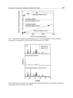
We have studied laser diodes operating at 975 nm and 894 nm wavelengths. The 975 nm
laser diode was based on three InGaAs quantum wells embedded in a GaAs waveguide.
The waveguide had an Al
0.6
Ga
0.4
As cladding layer, and a heavily doped GaAs contact
grown on top of the cladding. We used a third order grating period (~450 nm) to keep the
aspect ratio of the etching at a reasonable level (around 7.5). These lasers exhibited a high, 50
dB, side-mode suppression-ratio near the gain-grating resonance, and a 40 dB side-mode
suppression-ratio across the tuning area of 3 nm. The devices exhibited a wavelength
tunability of 77 pm/°C. The Light-Current-Voltage relation and spectrum graph of the of
one such device are shown in figure 10. The demonstrated laser diode is the first one
fabricated with soft UV-NIL.
Fig. 10. On the left: Light-Current-Voltage behavior of the DFB laser diode showing
threshold current of 30 mA and slope efficiency of 0.35 W/A. On the right: Spectrum of the
device measured at 5 mW, 10 mW and 15 mW output power.
Our lasers operating at 894 nm are designed for pumping the D1 transition of Cs-atoms.
They are based on a single GaInAs quantum well embedded in a GaInP-waveguide. The
waveguide had an Al
0.7
Ga
0.3
As cladding layer, and a heavily doped GaAs contact grown on
top of the cladding. Grating periods of 418.6 nm and 421.4 nm produce resonances at 888
nm and 894 nm, respectively. Tunability of the laser is 89 pm/°C. The Light-Current-Voltage
relation and spectrum graph of one of such is illustrated in figure 11.
Recent Optical and Photonic Technologies
292
Fig. 11. On the left: Light-Current-Voltage behavior of the DFB laser diode showing
threshold current of 15 mA and slope efficiency of 0.7 W/A. On the right: Spectrum of the
device showing the tunability around the D1 transition of Cs-atoms.
3.2 Plasmonic nanostructures
In recent years metallic nanostructures have been under intense investigation in the field of
nanophotonics as they enable the manipulation of light beyond the diffraction limit (Nature
Photonics 2008). In particular sharp particles are particularry attractive, as they can produce
highly localized electromagnetic fields due to a combination of plasmon resonances and the
so-called lightning rod effect. Strong local fields enhance light-matter interactions and have
various applications in tip-enhanced near-field microscopy, sensing, and nanofocusing of
light.
The main challenge with these nanostructures is their fabrication, especially in large volumes.
Electron beam lithography and focused ion beam (FIB) etching offer fast ways to producee
plasmonic structures, but they have limitations in the large volume patterning needed for
commercial applications. Here nanoimprint lithography has an advantage. It offers resolution
on the sub 10-nm scale and also enables rapid fabrication on the wafer scale with low cost
lithography equipment. The pattern can be replicated hundreds of times from the same stamp.
NIL is also much less damaging to the substrate compared to FIB, an essential feature in
patterning on top of compound semiconductor quantum well and dot structures.
Fig. 12. The principle of nanocone fabrication by NIL.
Using nanoimprint lithography we have fabricated conical nanostructures, nanocones, with
sharp tips and good uniformity (Fig. 13). In our tests we used a stamp with a 4 cm
2
pattern
area for imprinting. The final wafer consisted of ~4,0 x 10
9
nanocones and the yield of the
unoptimized process was 95 %. The principle of nanocone formation is similar to that used
Nanoimprint Lithography - Next Generation Nanopatterning Methods
for Nanophotonics Fabrication
293
to fabricate Spindt-type field emitters (Fig. 11, Spindt et al. 1968). Although the fabrication
process is quite simple and well-known in field emission applications, to the best of our
knowledge it has not been exploited in plasmonic applications. We demonstrated that the
nanocones lead to strongly localized electric fields which enhance nonlinear optical
properties (Kontio et al. 2009a). The second-harmonic (SH) signal was enhanced by a factor
of 150 compared to gold nanoparticles (half-cones) with the same period and base diameter,
but without a sharp tip (Fig. 13). Evidently the strongly localized electromagnetic field of the
fundamental beam enhances the SH signal. Possible application areas for metallic nanocones
include tip probes, sensors and metamaterials. We have also fabricated nanocones from
several different metals (Ag, Al, Au, Cr, Ge, Ni, Pt, and Ti) (Kontio et al. 2009b). The aspect
ratio and overall quality strongly depends on the evaporated material.
Fig. 13. On the left: A SEM image of an array of nanocones with a period of 300 nm, base
diameter 130 nm, and height 290 nm. On the right: A line scan of the second-harmonic
signal from the sharp nanocones and half-cones.
3.3 Patterned facets of optical fibres
Micro- and nanopattered surfaces of optical fibre can operate as various miniature optical
elements. They can modify the propagation of light by diffracting, collimating, shaping, or
focusing it. A properly designed optical element on the facet of an optical fibre improves the
functionality of the fibre without compromising the compactness of an optical system.
Miniaturized elements could subsequently be used for building miniature spectrometers,
sensors, and other devices. However, until now suitable nano- and microfabrication
methods that would allow efficient fabrication of such fibres have not existed.
So far, one simple optical element that can be prepared on the tip of a fibre is a lens. The lens
may be made by grinding or melting the end of the fibre, or combining segments of fibres
with different refractive index profiles (Shiraishi et al. 1997 and Yeh et al. 2004). More
complex elements containing small features are made by micro- and nanopatterning using
focused ion beam lithography or electron beam lithography (Giannini et al. 2000 and
Schiappelli et al. 2003). These direct writing methods are expensive to deploy and capital
investments are high. Moreover, their use for any small substrate, such as the facet of an
optical fibre, is challenging.
We have demonstrated the world’s first surface reliefs fabricated by NIL on the facet of a
single fibre by (Viheriälä et al. 2007). The method utilized UV-curable polymer that was
deposited on the facet by dip coating. Although dip coating delivers a rather non-repeatable
quantity of polymer on the facet, due to the small size of the fibre it is possible to press
excess low viscosity polymer away from the facet. We used polymer relief as the functional
Recent Optical and Photonic Technologies
294
element. This application only requires a simple imprint setup. The set-up is built built on
an optical table, and includes a stamp holder and micromanipulator for bringing fibre and
stamp into contact. A microscope was used to monitor the contact between the stamp and
the fibre in situ, since excess contact force easily bends the fibre between the fibre chuck and
the contact point. Polymer between the fibre and the stamp was cured with fibre-coupled
UV-source delivering immense UV-intensity of 8 W/cm
2
Intensities this high cure the UV-
NIL-polymer nearly instantaneously.
Using this simple set-up we patterned two sets of fibre facets. We used a standard single-
mode fibre (Corning SMF-28). The first set of samples was patterned using a commercially
available blazed grating with 830 lines / mm (Optometrics Corp). The second set of patterns
consisted of holes with diameters of 250 nm, arranged in a square lattice with a period of 500
nm. The blazed grating was used in order to study the diffraction efficiency of the imprint.
The grating efficiency was defined as the power of the first-order diffraction mode over the
total light power in the modes. Efficiency versus wavelength graph is plotted in figure 14.
Fig. 14. On left: SEM image illustrating the facet of the optical fibre with the imprinted
blazed grating. Insert: Close up near the fibre edge. On right: Graph of diffraction efficiency,
and image from the output of the fibre when white light is launched into fibre.
We also demonstrated that nanopatterning of the fibre tip is possible. We used a stamp
having 250 nm holes in a grid with a 500 nm period. The final structure showed good
uniformity. The standard deviance for the diameter of the holes was below 7 nm, as
analyzed from SEM images near the core of the fibre. We expect that that main mechanism
causing this diameter deviation was the template having standard deviation of this
magnitude. The very accurate replica obtained provides clear-cut evidence that UV-NIL can
produce flawless sub-wavelength features on a small area fibre facet. In work published
later, similar methods were also employed by other groups in order to fabricate fibre probes
for on-wafer optical probing (Scheerlinck et al., 2008) and to make fibres with integrated
surface enhanced Raman scattering sensors on their facet (Kostovski et al., 2009).
4. Conclusion
Nanophotonics is a rapidly growing field with great commercial potential. However, it is
not yet clear how fabrication for a myriad of different applications can be scaled up. The
electronics industry has developed its own fabrication methods largely around optical
lithography but it is clear that the same model can not automatically be used for photonics
fabrication. The field of nanophotonics is much more fragmented, less standardized, and
Nanoimprint Lithography - Next Generation Nanopatterning Methods
for Nanophotonics Fabrication
295
requires different technical specifications than electronics. We expect that NIL will play an
important role in the commercialization of many nanophotonics applications since it offers
excellent cost effectiveness and requires relatively low capital investment. We argue that in
many applications in particular UV-NIL based on soft working stamps is the best approach,
since it offers perhaps the best cost effectiveness. However, like any technology soft UV-NIL
has to be understood thoroughly before being applied to fabrication. We have underlined
some of the keys issues one may encounter when UV-NIL, and especially soft UV-NIL, is
applied and shown that, when NIL is mastered, it is possible to use it to demonstrate
various imprinted components.
5. Acknowledgements
The authors wish to acknowledge financial support from the Finnish Funding Agency for
Technology and Innovation within the projects Nanophotonics (161147-2) and Nano
Extension (40149/08), the European Space Agency within the project ESA GSTP
(21173/07/NL/PA), the EU within the FP7 project DeLight (224366) and the Academy of
Finland in the project A-Plan (123109) and Lightcaviti (115428). Jukka Viheriälä also wishes
to acknowledge the Ulla Tuominen Foundation, the Foundation for Financial and Technical
Sciences, the Finnish Foundation for Technical Promotion, the Cultural Foundation and the
National Graduate School in Materials Physics.
The authors also wish to thank MSc Tuomo Rytkönen, Mr Juha Tommila and Ms Milla-Riina
Viljanen for their invaluable work with Nanoimprint Lithograpy, Mr Aki Wallenius and Mr
Jarkko Telkkälä for their work with DFB-Laser diodes, and MSc Kimmo Harring for skillful
preparation of optical coatings. Dr Charis Reith has had an important role in proofreading
the English text. Without support from the epitaxy group - Dr Tomi Leinonen, MSc Lauri
Toikkanen, MSc Teemu Hakkarainen and Ms Sanna Ranta - work with laser diodes would
have been impossible. Optical design of the laser diodes was carried out by MSc Antti
Laakso and Dr Mihail Dumitrescu. The authors acknowledge Dr Janne Simonen and Dr
Mihail Dumitrescu as important forces in driving plasmonics and laser diode research
forward. Finally we wish to acknowledge people that have prepared various NIL templates
for our activities. Of these people we wish to especially acknowledge the University of
Joensuu physics department : Prof Markku Kuittinen, Dr Hemmo Tuovinen, Dr Janne
Laukkanen, MSc Kari Leinonen, MSc Ismo Vartiainen and XLith GmbH, AMO GmbH and
Chalmers technical university.
6. References
Abe H., Ayling S. G., Marsh J. H., De La Rue R. M., and Roberts J. S. (1995). Single-mode
operation of a surface grating distributed feedback GaAs-AlGaAs laser with
variable-width waveguide, IEEE Photon Technol. Lett., Vol. 7, No. 5, pp. 452–454
Austin M. D., Zhang W., Ge H., Wasserman D., Lyon S. A. and Chou S. Y. (2005). 6 nm half-
pitch lines and 0.04 µm
2
static random access memory patterns by nanoimprint
lithography, Nanotechnology, Vol. 16, pp. 1058-1061
ASML (2009). ASML, TWINSCAN™ NXT:1950i specifications
Bird R. B., Armstrong R. C. and Hassager O. (1977). Dynamics of Polymer Liquids, Fluid
Mechanics, Vol. 1, John Wiley & Sons, 1977
Recent Optical and Photonic Technologies
296
Brooks C., Schmid G., Miller M., LaBrake D., Hofemann P., Resnick D., Sreenivasan S.V.
(2009). Patterned Media Using Step and Flash Imprint Lithography, SPIE Advaned
Lithography Conf., Alternative Lithographic Technologies, Proc. of SPIE, Vol. 7271,
72711L, San Jose, USA, 2009
Choi K.M. and Rogers J.A. (2003). A Photocurable Poly(dimethylsiloxane) Chemistry
Designed for Soft Lithographic Molding and Printing in the Nanometer Regime, J.
Am. Chem. Soc., Vol. 125, No. 14, pp. 4060-4061
Chou S. Y., Krauss P. R., and Renstrom P. J. (1995). Imprint of sub-25 nm vias and trenches
in polymers, Appl. Phys. Lett. Vol. 67, pp. 3114-3116
Chou S. Y., Krauss P. R., Zhang W.,Guo L. and Zhuang L. (1997). Sub-10nm imprint
lithography and applications, J. Vac. Sci. Technology B, Vol. 15, pp. 2897-2904
Dow Corning (2009). Sylgard® 184 silicone elastomer kit, product datasheets, electronics
French R. H., Sewell H., Yang M. K., Peng S., McCafferty D. C., Qiu W., Wheland R. C.,
Lemon M. F., Markoya L. and Crawford M. K. (2005). Imaging of 32-nm 1:1 lines
and spaces using 193-nm immersion interference lithography with second-
generation immersion fluids to achieve a numerical aperture of 1.5 and a k
1
of 0.25,
Journal of Micro/Nanolithography, MEMS, and MOEMS, Vol. 4, No. 3, 031103
Fuard D., Tzvetkova-Chevolleau T., Decossas S., Tracqui P. and Schiavone P. (2008),
Optimization of poly-di-methyl-siloxane (PDMS) substrates for studying cellular
adhesion and motility, Microelectronic Engineering, Vol. 85 No. 5-6, pp. 1289-1293
Gelest Inc. (2009). Silicone coatings, encapsulats, gels. Performance property guide for
Dielectric, Optical, Thermal and Mechanical applications
Giannini G., Mastrogiacomo L., Cabrini S., Gerardino A., Nottola A., Foglietti V. and Cianci
E. (2000). Microfabrication of diffractive optical elements onto the active region of
optical fiber termination, in Proc. MICRO tec.2000 VDE World Microtechnologies
Congress, vol. 2, pp. 695-7, Berlin, Germany, 2000
Glinsner T., Plachetka U., Matthias T., Wimplinger M. and Lindner P. (2007). Soft UV-based
nanoimprint lithography for large-area imprinting applications, Emerging
Lithographic Technologies XI. Proceedings of the SPIE, Vol. 6517, pp. 651718
Golka S., Pflügl C., Schrenk W., and Strasser G. (2005). Quantum cascade lasers with lateral
double-sided distributed feedback grating, Appl. Phys. Lett. Vol. 86, 111103
Houle F. A., Rettner C. T., Miller D. C., and Sooriyakumaran R. (2007). Antiadhesion
considerations for UV nanoimprint lithography, Appl. Phys. Lett., Vol. 90, 213103
Hua F., Sun Y., Gaur A., Meitl M. A., Bilhaut L., Rotkina L., Wang J., Geil P., Shim M. and
Rogers J. A. (2004), Polymer Imprint Lithography with Molecular-Scale Resolution,
Nano Letters, Vol. 4, No. 12, pp. 2467-2471
Kang H., Lee J., Park J. and Lee H. H. (2006). An improved method of preparing composite
poly(dimethylsiloxane) moulds, Nanotechnology, Vol. 17, pp. 197–200
Anna Klukowska A., Kolander A., Bergmair I., Mühlberger M., Leichtfried H., Reuther F.,
Grützner G. and Schöftner R. (2009), Novel transparent hybrid polymer working
stamp for UV-imprinting, Microelectronic Engineering, Vol. 86, No. 4-6, pp. 697-699
Kontio J.M, Husu H, Simonen J., Huttunen M.J, Tommila J., Pessa M., and Kauranen M.
(2009a), Nanoimprint fabrication of gold nanocones with ~10 nm tips for enhanced
optical interactions, Optics Letters, Vol. 34, pp. 1979–1981
Nanoimprint Lithography - Next Generation Nanopatterning Methods
for Nanophotonics Fabrication
297
Kontio J.M., Simonen J., Tommila J., and Pessa M. (2009b). Arrays of metallic nanocones
fabricated by UV-nanoimprint lithography, Article in Press, Microelectronic
Engineering
Koo N., Bender M., Plachetka U., Fuchs A., Wahlbrink T., Bolten J. and Kurz H. (2007).
Improved mold fabrication for the definition of high quality nanopatterns by Soft
UV-Nanoimprint lithography using diluted PDMS material, Microelectronic
Engineering, Vol. 84, pp. 904-908,
Kostovski G., White D.J., Mitchell A., Austin M.W. and Stoddart P.R. (2009). Nanoimprinted
optical fibres: Biotemplated nanostructures for SERS sensing, Biosensors and
Bioelectronics, Vol 24, No. 5, pp. 1531-1535
Levola T. and Laakkonen P. (2007). Replicated slanted gratings with a high refractive index
material for in and outcoupling of light, Optics Express, Vol. 15, pp. 2067-2074
Nature Photonics Issue “Antennas of Light” (2008), Nature Photonics, Vol. 4, pp. 199
Petric P., Bevis C., Brodie A., Carroll A., Cheung A., Grella L., McCord M., Percy H.,
Standiford K., and Zywno M. (2009). REBL Nanowriter: Reflective Electron Beam
Lithography, Advanced Lithography, Proc. of SPIE Vol. 7271 727107-1, San Jose,
USA, 2009
Pozzi F., De La Rue R. M., and Sorel M. (2006). Dual-Wavelength InAlGaAs–InP Laterally
Coupled Distributed Feedback Laser, IEEE Photon Technol. Lett., Vol. 18, No. 24, pp.
2563-2565,
Mapper Lithography (2009). Press Release 2008,
Checked 1.6.2009
Micro Resist Technology (2009a). Preliminary process guidelines, contact person: Anna
Klukowska
Micro Resist Technology (2009b). Ormocer®s (hybrid polymers) for micro optics, product
flyer
Scheerlinck S., Taillaert D., Van Thourhout D., Baets R. (2008). Flexible metal grating based
optical fiber probe for photonic integrated circuits, Appl. Phys. Lett., Vol. 92
pp.031104
Schiappelli F., Prasciolu M., Cojoc D., Cabrini S. and Di Fabrizio E. (2003). Design and
fabrication of lenses on the top of an optical fiber for efficient fiber-to-waveguide
coupling by means of Focus Ion Beam (FIB) lithography, in Dig. of Papers
Microprocesses and Nanotechnology, pp. 166-167., Int. Microprocesses and
Nanotechnol. Conf., Tokyo, 2003
Schmid H. and Michel B. (2000). Siloxane Polymers for High-Resolution, High-Accuracy Soft
Lithography. Macromolecules, Vol. 33 pp. 3042-3049
Schuster C., Reuther F., Kolander A., Gruetzner G. (2009). mr-NIL 6000LT – Epoxy-based
curing resist for combined thermal and UV nanoimprint lithography below 50 °C ,
Microelectronic Engineering, Vol. 86, No. 4-6, pp. 722-725
Shiraishi K., Ohnuki H., Hiraguri N., Matsumura K., Ohishi I., Morichi H. and Kazami H.
(1997). J. Lightw. Technol., Vol. 15, 1997, pp. 356-363.
Sorel M., Strain M. and Mezosi G. (2008). Semiconductor ring lasers for ultra fast all-optical
digital processing, European Semiconductor Laser Workshop 2008, Eindhoven,
Netherlands, 9th – 20th September, 2008
Solak H. H., Ekinci Y., Käser P. and Park S. (2007). Photon-beam lithography reaches 12.5
nm half-pitch resolution, J. Vac. Sci. Technol. B, Vol. 25, No. 1, pp. 91-95
Recent Optical and Photonic Technologies
298
Spindt C.A. (1968). A Thin-Film Field-Emission Cathode, Journal of Applied Physics, Vol. 39,
pp. 3504
Sreenivasan S.V., Schimaker P., Mokaberi B., Choi J., Perez J., Truskett V., Xu F., Lu X.
(2009). Recent Developments in UV Nanoimprint Stepper Technology for Sub-
30nm Half-Pitch Lithography, SPIE Advaned Lithography Conf., Proc. of SPIE Vol.
7271, San Jose, USA, February, 2009
Sumitomo (2009). Sumitomo Electric, GaAs and InP wafer flatness specifications, 19.1.2009.
“
Suss Microtech (2009). Spesfications for automatic and semiautomatic mask aligners
Technology review (2003), 10 Emerging Technologies That Will Change the World,
Technology review, Vol. 38, Ferbruary 2003
Viheriälä J., Niemi T., Kontio J., Rytkönen T. and Pessa M. (2007). Fabrication of surface
reliefs on facets of singlemode optical fibres using nanoimprint lithography,
Electronics letters, Vol. 43, No. 3, pp. 150-152
Viheriälä J., Rytkönen T., Niemi T. and Pessa M. (2008). Narrow linewidth templates for
nanoimprint lithography utilizing conformal deposition, Nanotechnology, Vol. 19,
015302
Viheriälä J., Tommila J., Leinonen T., Dumitrescu M., Toikkanen L., Niemi T. and Pessa M.
(2009). Applications of UV-nanoimprint soft stamps in fabrication of single-
frequency diode lasers, Microelectronic Engineering, Vol. 86, No. 3, pp. 321-324
Viheriälä J., Viljanen M R., Kontio J., Leinonen T., Tommila J., Dumitrescu M., Niemi T. and
Pessa M. (2009b). Soft Stamp UV-Nanoimprint Lithography for Fabrication of Laser
diodes, Journal of Micro/Nanolithography, MEMS, and MOEMS, Vol. 8, 033004
Wieland M.J., de Boer G., ten Berge G.F., Jager R., van de Peut T., Peijster J.J.M., Slot E.,
Steenbrink S.W.H.K., Teepen T.F., van Veen A.H.V., Kampherbeek B.J. (2009).
MAPPER: High throughput maskless lithography, Alternative Lithographic
Technologies, Proc. of SPIE Vol. 7271, 72710O, San Jose, USA, 2009
Williams B. S., Kumar S., John Q. H. and Reno L. (2005). Distributed-feedback terahertz
quantum-cascade lasers with laterally corrugated metal waveguides, Optics Letters,
Vol. 30 No. 21, pp. 2909-2911
Yeh S M., Lu Y K., Huang S Y., Lin H H., Hsieh C H., and Cheng W H (2004) A novel
scheme of lensed fiber employing a quadrangular-pyramid-shaped fiber endface
for coupling between high-power laser diodes and single-mode fibers, J. Lightw.
Technol., Vol. 22, No. 5, pp. 1374-1379.
15
Nanoscale Photodetector Array and Its
Application to Near-Field Nano-Imaging
Boyang Liu
1
, Ki Young Kim
1,2
, and Seng-Tiong Ho
1
1
Department of Electrical Engineering and Computer Science, Northwestern University
2
Department of Physics, National Cheng Kung University
1
USA
2
Taiwan
1. Introduction
Photodetector array have many applications, such as light detection and imaging. However,
pixels in most photodetector array are micrometer scale or larger, which limits its
application to relatively low spatial resolution detection. The possibility to realize
photodetector array with pixel size at nanometer scale has become of great interest to
various technologies. When the dimension of photodetector array’s pixel is reduced to such
a small scale, many new functions can be achieved. For example, with such a nanoscale
photodetector array, it will enable us to image objects at a resolution better than that of
conventional diffraction-limited imaging tool, for which the highest resolution that could be
obtained is half of the illuminating light wavelength. Recently, many progresses on nano-
scale photodetector array (NPD) have been made (Huang et al., 2001; Hayden et al., 2006;
Yang et al., 2006; Maier et al., 2003), however most of them are based on nanotube
technology and incapable of precisely controlling the position and configuration of detector
array. It’s desirable to have a photodetector array with nanoscale pixels while still having
flexibility in device design and operation. In this chapter, we will present the research on
such a photodetector array with nano-scale pixels based on dual side metal-semiconductor-
metal (MSM) structure, including the design of NPD array, the simulation of NPD array’s
performance by finite difference time-domain (FDTD) method, the fabrication of NPD
device, characterization of NPD array and the demonstration of nano-scale object imaging
using the NPD array that fabricated.
2. Design of nanophotodetector array
The design of NPD array has a basic structure shown in Fig. 1. In
0.53
Ga
0.47
As ternary
material is chosen as absorbing material for near-IR (1.0-1.6 µm) wavelength range
detection. A dual side MSM structure is employed, where the semiconductor active material
is sandwiched by the top and bottom electrode. The top and bottom electrode stripes are
perpendicular to each other, which enables the pixel addressing by NPD array. Concerns
and considerations for these configurations are described under the following categories: (1)
selection of active material and structure; (2) considerations in choosing MSM structure.
Recent Optical and Photonic Technologies
300
TCO
Metal/TCO
BCB BCB
Semi-
conductor
Metal/TCO Metal/TCO
Semi-
conductor
Semi-
conductor
Bottom Receiving Electrode
Top
Electrode
BCB BCB
Semi
conductor
Semi
conductor
Semi
conductor
Illumination Light
Top
Electrode
Top
Electrode
Fig. 1. The schematic of the novel NPD array design, where Benzocyclobutene (BCB) fills all
areas between NPD array pixels.
2.1 Selection of active material and structures
Commonly, GaAs material is used for 0.8 µm wavelength detection and has demonstrated a
good performance (Biyikli et al., 2001; Biyikli et al., 2004; Seo et al., 1992). For near-IR (1.0-1.6
µm) wavelength range, typically In
0.53
Ga
0.47
As, AlGaAs, InGaP and In
0.52
Al
0.48
As are chosen
as active material (Biyiklia et al., 2003; Chyi et al., 1994; DeCorby et al., 1997; Gao et al., 1994;
Gao et al., 1995; Gao et al., 1997; Kim et al., 1998; Loualiche et al., 1990; Zhao et al., 2007). In
practical application, In
0.53
Ga
0.47
As ternary compound is chosen as active material due to its
band gap energy of 0.8 eV and lattice matching to InP material which has extensive
applications in optical communications.
However, in near-IR region, the In
0.53
Ga
0.47
As MSM photodetectors have not performed
well. The primary difficulty is the low schottky barrier height (~0.2 eV) of commonly used
Schottky contact metals on In
0.53
Ga
0.47
As (Griem et al., 1990). Low barrier height results in
excessive dark current and noise. One solution is to add an enhancement layer between the
metal and In
0.53
Ga
0.47
As absorbing layer to increase the Schottky barrier height. As a result, a
Schottky barrier enhancement layer is used, i.e. digitally graded InAlAs/InGaAs super
lattice (SL). The SL structure used is shown in Fig. 2. The graded super lattice consists of 3
periods of In
0.52
Al
0.48
As and In
0.53
Ga
0.47
As, whereby the first period is composed of 7 nm of
In
0.53
Ga
0.47
As and 3 nm of In
0.52
Al
0.48
As, and the last period is reversed with 3 nm of
In
0.53
Ga
0.47
As and 7 nm of In
0.52
Al
0.48
As. The intermediary layer varies linearly between two
endpoints in 2 nm increments. The graded SL structure is then capped with an additional
50nm i-In
0.52
Al
0.48
As Schottky barrier enhancement layer.
2.2 Metal-Semiconductor-Metal structure
Metal-Semiconductor-Metal photodetector structure is equivalent to two Schottky diodes
back to back, shown in Fig. 3. Their response is related to the current caused by the electron-
hole pairs separated by the electric field in the depletion region of two Schottky diodes
(Land et al., 1985). These devices usually have a simple planar design, often with
interdigitated (IDT) fingers structure. The IDT MSM photodetector’s respond speed is
typically determined by the transit time rather than RC constant.
In practice, a dual side MSM structure is employed, where geometry with electrodes above
and below a thin-layer of intrinsic semiconductor as active material is used for pixel
Nanoscale Photodetector Array and Its Application to Near-Field Nano-Imaging
301
InAlAs/InGaAs Grading layer (30nm)
InAlAs/InGaAs Grading layer (30nm)
InAlAs (50nm)
InGaAs Active layer (300nm)
InAlAs (50nm)
InGaAs etch-stop layer (200nm)
InP Substrate
460nm
In
0.52
Al
0.47
As –7nm
In
0.53
Ga
0.48
As –3nm
In
0.52
Al
0.47
As –7nm
In
0.53
Ga
0.48
As –3nm
In
0.52
Al
0.47
As –7nm
In
0.53
Ga
0.48
As –3nm
InAlAs/InGaAs Grading layer (30nm)
Fig. 2. Structure scheme of practical InGaAs active region with In
0.52
Al
0.48
As Schottky barrier
enhancement layer using digitally graded SL as transition layer.
-10 -5 0 5 10
-0.3
-0.2
-0.1
0.0
0.1
0.2
0.3
Ι (μΑ)
Voltage (V)
Fig. 3. MSM structure photodetector is equivalent to two Schottky diodes back to back.
addressing (shown in Fig. 4.). To detect a certain pixel, we will just connect to the right top
and bottom electrode stripes. The detector where the top and bottom electrode stripe crosses
will be the one that is sensed by the detector circuit. Thus, using M+N stripes, we can
address M x N pixels.
3. Finite-difference time-domain simulation of nanophotodetector array
In this section, highest possible resolution obtainable with the proposed imaging array
shown in Fig. 4 is investigated using the finite-difference time-domain method. The FDTD
method (Yee 1966) is one of widely used numerical techniques in simulations for various
optoelectronic and photonic devices. However, due to the lack of proper active
semiconductor model for photonics applications, conventional FDTD simulations are yet
Recent Optical and Photonic Technologies
302
Metal
Semicon
ductor
To p Electr o de
Bottom
Electrode
Illumination
Semicon
ductor
(a) (b)
Fig. 4. (a) 3D schematic for channelized NPD array, where the front electrode stripes have a
crossing direction to the back side electrodes, forming a matrix for pixel addressing; (b) Top
view of a 4 x 4 NPD array.
simple enough while still taking into account the physics of semiconductor materials. A new
idea using multi-level multi-electron (MLME) semiconductor FDTD model has been
developed by Huang and Ho (Huang 2002; Huang & Ho 2006), in which multiple energy band
levels to describe the essential characteristics of the semiconductor energy band structures
have been incorporated. This simulation scheme has also been successfully utilized in various
photonic device applications with active semiconductors including photodetector, photonic
crystal fiber, photonic transistor, whispering gallery resonator, and so on (Kim et al. 2008; Khoo
et al. 2008). In order to understand the working mechanism of NPD array as a nanoscale
imaging device, a MLME FDTD method has been adopted in this Chapter.
Fig. 5. Generation of photocurrent from photoelectrons in active semiconductor material.
λ
=
λ
a
=1550 nm is assumed, where
λ
and
λ
a
are the incident wavelength and resonant
wavelength of the active semiconductor material, respectively.
Nanoscale Photodetector Array and Its Application to Near-Field Nano-Imaging
303
In the FDTD simulations for the NPD array, photocurrent generated in semiconductor
material by the incident light is one of key parameters in evaluating performance of a
photodetector. The photocurrent generated in the active semiconductor medium is
dependent on the incident (excitation) wavelength and the energy band gap structure of the
semiconductor material. Conceptually, an active semiconductor material for photodetectors
can be simplified as a medium with two different energy levels, in which the photocurrent
can be calculated from the rate of excitation of ground state electrons from the ground level
to the excitation level, which are subsequently retuned back to the ground level via external
electric circuit as shown in Fig. 5. In Fig. 5, electrons in ground state (level 1) are excited and
transited to excited state (level 2), when the incidence wavelength is matched to inherent
resonance wavelength of an active semiconductor material. Here, we assumed
λ
=
λ
a
=1550nm, where
λ
and
λ
a
are incidence wavelength and resonance wavelength of an
active semiconductor, respectively, which belongs to an optical telecommunication
wavelength.
For conducting numerical simulations with the MLME FDTD code, the active
semiconductor material needs to be spatially discretized as shown in Fig. 6, as well as other
parts of the present device. The photocurrent generated in an active semiconductor material,
which is composed of numerous FDTD pixels, can be quantitatively calculated from the
following formula, which has been directly given based on the definition of the typical
concept of electric current and photocurrent mechanism shown in Fig. 5.
2ph density
pixel
sim sim
IN NNAh
tt
⎛⎞
=
=⋅⋅⋅
⎜⎟
⎝⎠
∑
, (1)
where
19
1.6 10qC
−
=× is the electric charge, t
sim
is the total time simulated, N
2
is the
normalized number of electrons in the level 2 in a single FDTD cell, N
density
is the number of
electrons per unit volume, A is the area of the FDTD pixel, and h is the height of the NPD
pixel. Here, we set t
sim
=1.0 ps, N
density
=0.563x10
22
/m
3
, A=dx x dy=5 nm x 5 nm, and h=300 nm
considering a dimension for fabrication.
FDTD pixel
Light
excitation
photoelectrons
dx
dy
semiconductor
Fig. 6. Discretization of an active semiconductor material for the MLME FDTD method.
Photoelectrons in each pixel are generated by light illumination. Photocurrents can be
calculated with the photoelectrons.
Recent Optical and Photonic Technologies
304
Fig. 7. Simplified two-dimensional schematic illustration of the NPD array.
InGaAs is used as active semiconductor regions of the NPD array. A protective material
such as benzocyclobutene (BCB) is filled between pixels to support device structures and
form cladding layer to each pixel. Top and bottom electrodes are placed at front and
backside of the array for the purpose of photocurrent pickup to external electric circuit to
detect the photocurrent generated in each pixel of the NPD array. Bottom electrode could be
either a transparent conducting oxide (TCO) or a thin metal layer for light passing through.
The refractive indexes of InGaAs, BCB, and air at 1550 nm are assumed to be 3.4, 1.5, and
1.0, respectively.
Fig. 7 illustrates a simplified two-dimensional schematic of the NPD array for clearer
description of its working principles for a practical photocurrent pickup mechanism. The
active semiconductor material slabs, where photoelectrons are generated by the incident
light as described in Fig. 5 and 6, are separated by protective material with lower refractive
index that forms cladding layer to each NPD pixel and supports the device structure
mechanically. The active semiconductor layer is sandwiched between the top and bottom
electrodes. Top and bottom electrodes are placed at front and backside of the array for the
purpose of photocurrent pickup to external electric circuit to detect the photocurrent
generated in each pixel of the NPD array. Very thin layer of metal layer or optically
transparent conductor such as transparent conducting oxide (TCO) will be used for the
bottom electrode, forming a matrix with top metal electrodes for pixel-array addressing as
shown in Fig. 4. In our NPD design, the active semiconductor region is made from InGaAs
with refractive index of 3.4 and surrounded by BCB with refractive index of 1.5. In working
condition, the active semiconductor materials in NPD pixels get excited by the near-field
point-like light source, which will cause an increase of active material’s conductivity and
increase the electric current of detection circuit. Therefore, the photocurrent generated by
each pixel is the signal of the NPD imaging device. If we define the width of NPD pixel as w
and spacing between two adjacent pixels as s, the w+s would be the resolution of the NPD
array imaging. In our study, the 1/e (~36.79%) resolution criterion is used for NPD imaging
characterization. If we assume the photocurrent generated by the mth NPD pixel as 1.0,
when the generated photocurrent by the (m+1)th or (m-1)th pixel is less than 1/e, we say the
mth pixel and the (m+1)th or (m-1)th pixel can be distinguishable from each other. For
Nanoscale Photodetector Array and Its Application to Near-Field Nano-Imaging
305
example, if the photocurrents generated in pixels 0 and 1 are 100 nA and 30 nA,
respectively, we will have the ratio of 30% that is less than 1/e. Then, these two pixels are
distinguishable.
Fig. 8. The schematic of the NPD array with its dimensions for the FDTD simulation. Light
to be detected is from the subwavelength metal slit. NPD pixels are labelled as 0, 1, 2, 3, and
4.
Fig. 8 shows a two-dimensional schematic illustration of the NPD array for our MLME
FDTD simulations. The light of 1550 nm is incident from the bottom side. We assume a
detector slab that is infinite in the direction perpendicular to the paper and the incident
source has electric field polarization pointing along this infinite direction. The center-to
center distance between the NPD pixels is w+s with a width of the NPD pixel of w and an
inter-pixel gap of s, as same as in Fig. 7. The length of the NPD pixels is set to be 3.0
μ
m to
investigate the optical power coupling between pixels, although in practical fabrication, the
length of NPD pixels is only a few hundred of nanometers. The semiconductor fingers
(pixels) play an important role in detecting incident field, which are converted into
photocurrent via the mechanism shown in Fig. 5.
The placement of the imaging device to immediately proximate distance from the near-field
light source within a few nanometer orders is strongly required to avoid rapid fading-out of
the near-field light. Since all practical NPD devices will work in the near-field region of the
illuminating light, the distance between aperture and the NPD array is set to be 10 nm,
which assures that central pixels are within the near-field region of the light from aperture.
To generate the near-field point-like source, we block the incident plane wave of 1550 nm by
a metal film with a small aperture having a small width (a). The front side of the center pixel
of the NPD array has been placed at very near distance away from the aperture, thereby, the
NPD array can pick up the light from the aperture having diffraction-limited subwavelength
light.
The photocurrents from the NPD pixels are obtained to explore the resolution of this novel
NPD device for subwavelength diffraction limited imaging. One limiting factor is the optical
Recent Optical and Photonic Technologies
306
power coupling between adjacent detector pixels. The MLME FDTD simulation enables us
to investigate such power coupling in the presence of absorbing media as well as the spatial
distributions of electric field and photoelectron density.
(a) (b)
Fig. 9. (a) Simulation of NPD array by conventional FDTD method. The NPD pixel is 200nm
wide with 50 nm spacing. The highest resolution is 250 nm for 1550 nm wavelength; (b)
simulation of NPD array by MLME FDTD method, the NPD pixel is 100 nm wide with
50nm spacing. The highest resolution is 150 nm for 1550 nm wavelength.
In order to investigate the effect of the optical absorption in optical energy coupling between
adjacent pixels in the NPD array, both conventional FDTD and MLME FDTD models are
used and results for both cases are compared with each other in Fig. 9. In conventional
FDTD simulation, only optical energy in each NPD pixel could be simulated, where the light
propagates in dielectric NPD pixels and no interactions between light and NPD detection
region are considered. Simulation shows a highest resolution of 250 nm, shown in Fig. 9(a).
On the contrary, in MLME FDTD simulation, both the optical energy and photocurrent
generated in each pixel could be simulated. Before simulation, the number density of active
semiconductor material in MLME FDTD model is calibrated to match real property of
InGaAs semiconductor to be used in experiments for 1550 nm wavelength. The calibrated
active material loss of around 0.5/
μ
m for a typical III-V semiconductor material, which is
corresponding to a value N
density
=0.563x10
22
/m
3
in eq. (1) as mentioned earlier. Shown in Fig.
9(b), MLME FDTD simulation shows a highest resolution of 150 nm, which is 100 nm (60%)
higher than that by the conventional FDTD simulation. Compared with conventional FDTD
model, the MLME FDTD simulation shows a better matching to the response of
photosensitive material, which could be used to effectively simulate the photodetection
process by the photodetectors.
In order to investigate the optical power coupling between NPD pixels, the average optical
power in each pixel is calculated for the case of Fig. 9(b). Fig. 10(a) shows the electric field
distributions, which indicates electric field is quasi-bounded by the center pixel (pixel 0)
with subsequent coupling to the adjacent pixels (pixel 1, 2) and then to the next adjacent
pixels (pixel 3, 4). Fig. 10(b) shows the corresponding photoelectron density of the whole
NPD array from the electric field distributions of Fig. 10(a) with an arbitrary normalized
linear scale, where most of the photocurrent is generated by the central pixel.
Nanoscale Photodetector Array and Its Application to Near-Field Nano-Imaging
307
Fig. 10. (a) Electric field distributions and (b) corresponding normalized photoelectron
density distributions obtained with MLME FDTD simulation in NPD array configuration.
The dark red color indicates higher amplitude in arbitrary linear scale.
0 150 300 450 600 750 900
0.0
0.2
0.4
0.6
0.8
1.0
(nm)
100%
150nm
33%
Optical Energy
Position of Pixels
Fig. 11. Photocurrents generated in each NPD pixel.
Fig. 11 shows the photocurrents generated in each pixel from the spatial distribution of the
photoelectron density profile of Fig. 10(b) by using eq. (1), where the photocurrent in each
pixel for the 150 nm imaging resolution case, where the photocurrent generated in pixels
adjacent to central pixel is less than 33% (< 1/e criterion) of that in central pixel.
The photocurrent in each pixel has been normalized to that in the central pixel. The
estimated spatial resolution for this NPD array geometry is about 150 nm, which
corresponds to a resolution of
λ
/10. The resolution of 150 nm by NPD array corresponds to
about
λ
/10 for near-IR wavelength and about 25 times higher than the diffraction limited
conventional imaging system in terms of imaging area.
Recent Optical and Photonic Technologies
308
The achieved optical resolution is substantially below the subwavelength diffraction-limit of
λ
/2, which can be potentially applied to the observation of nano-scale moving objects or
living cells.
4. Nanofabrication of the NPD Array
4.1 Fabrication of NPD array
Several techniques to fabricate such a nano-imaging device have been developed to realize
the 3-dimentional structure of NPD array, including BCB wafer bonding technique and
metal oxide sol-gel based nanoscale direct patterning technique (B. Liu et al., 2008a, b) . The
pixel width and spacing of NPD array varies from 100 nm to 400 nm. A layer of Au/Ti (55
nm/5 nm) metal was deposited as receiving bottom electrodes. Up to 4×4 NPD array have
been fabricated, where the smallest array pixel is as small as 100 nm wide with 100 nm
spacing. Fig. 12(a) shows the top view of example 2×2 and 4×4 nanophotodetector array,
where the bright electrodes are bottom receiving electrodes and the dark ones are front
electrodes. An In
0.53
Ga
0.47
As based super lattice structure with 460 nm thickness is
sandwiched between the top and bottom electrode stripes. The Au/Ti top and bottom
electrode stripes are perpendicular to each other and form an addressable pixel array. Fig.
12(b) shows the detection region of a 4×4 NPD array, the pixel width is 400 nm wide with
400 nm spacing.
(a) (b)
Fig. 12. (a) The top view of 2×2 and 4×4 nanophotodetector array, where the dark electrodes
are front electrodes and the bright ones are back electrodes; (b) The detection region of a
4×4 NPD array.
4.2 Device packaging of nanoscale photodetector array
Packaging is of great importance for the characterization of photonic devices, especially
when the size of devices is down to the nanometer scale. Since each NPD device only has a
size no more than 1 mm × 1 mm square, to successfully cleave the NPD array into
individual pieces the thickness of each NPD array device has to be at least 4~5 times smaller
than the width of each NPD array device. Otherwise, the cleaving machine has to cut the
device wafer deep in order to make a successful cleaving, which will easily cause the
damage of the tiny NPD device and more debris during cleaving. Therefore, before cleaving,
the whole wafer that carries the NPD array devices were polished down to ~150 μm thick.
Nanoscale Photodetector Array and Its Application to Near-Field Nano-Imaging
309
In addition to cleaving process, bonding is also very important to the NPD device’s
performance. The quality of bonding will have a great influence on the electrical
performance and thermal conductivity of NPD device, especially for devices as small as a
few hundred nanometers. In practice, a sliver paste is used to connect the NPD electrodes
and extended electrodes. Fig. 13 shows the schematic of a bonded 4x4 NPD array using
silver paste.
15mm
15mm
D=1mm Copper pad
D=2mm Copper pad
Wire bonding gold wire
Fig. 13. The schematic of a bonded 4x4 NPD array.
5. Characterization and results
5.1 Photoresponse characterization
The electrical characterization of NPD array, which have pixel size of a few hundred
nanometers, is different from micrometer scale MSM detectors. The primary reason is the
small pixel size of NPD array. There are two main concerns on NPD characterization listed
below:
(a) The conventional planar IDT MSM structure photodetector has tens of or even more pixels
working together, which leads to a large detection area of hundreds of square micrometers or
even larger. As a result, it could generate relative large photoresponse signals of typically
around microamperes level. On the contrary, in order to enable the pixel addressing function,
each pixel in NPD array has to work individually. Since the NPD pixel has a size of a few
hundred nanometers and detection area is only a fraction of square micrometers, the
generated photoresponse signal by NPD pixel is very small. For instance, the estimated signal
of a single NPD array pixel could be as small as tens of picoamperes. However, the advantage
of NPD array pixels with small size is its corresponding low dark current.
(b) Since the NPD array has pixel size of a few hundred nanometers, the corresponding
detection area is only a fraction of square micrometers, which is already beyond the
focusing limit of the optical objective lens used to focus the illuminating light onto the NPD