Advances in Optical and Photonic Devices 2011 Part 4 pptx
Bạn đang xem bản rút gọn của tài liệu. Xem và tải ngay bản đầy đủ của tài liệu tại đây (5.54 MB, 25 trang )
Advances in Optical and Photonic Devices
66
Shimizu, H.; & Nakano, Y. (2006) Proceeding of 2006 International Semiconductor Laser
Conference, (Sep. 2006) TuA6.
Shimizu, H.; & Nakano, Y. (2007) IEEE. Photon. Tech. Lett., Vol. 19, No. 24, (Dec. 2007) 1973-
1975.
5
Optical Injection-Locking of VCSELs
Ahmad Hayat, Alexandre Bacou,
Angélique Rissons and Jean-Claude Mollier
Institut Supérieur de l’Aéronautique et de l’Espace (ISAE),
Toulouse
France
1. Introduction
Since the telecommunication revolution in the early 90s, that saw massive deployment of
optical fibre for high bit rate communications, coherent optical sources have made
tremendous technological advances. The technological improvement has been multi
dimensional; component sizes have been reduced, conversion efficiencies increased, power
consumptions decreased and integrability into compact optoelectronic sub-modules
improved. Semiconductor lasers, emitting in the 1.1-1.6 μm range, have been the most
prominent beneficiaries of these technological advances. This progress is a result of research
efforts that consistently came up with innovative solutions and components, to meet the
market demand. This in-phase, demand and supply, problem and solution and consumer
need and innovation cycle, has ushered us in to the present information technology era,
where stable high speed data links make the backbone of almost every aspect of life, from
economy to entertainment and from health sector to defence production.
By the start of twenty-first century, a new, low cost, low power consumption and
miniaturized generation of lasers had started to capture its own market share. These lasers,
named Vertical-Cavity Surface-Emitting Lasers (VCSELs) due to the presence of an optical
cavity which is normal to the fabrication plane , have established themselves as premier
optical sources in short-haul communications such as Gigabit Ethernet, in optical computing
architectures and in optical sensors. While shorter wavelength VCSEL (< 1μm) fabrication
technology was readily mastered, due to the ease in manipulation of AlGaAs-based
materials, long wavelength VCSELs especially VCSELs emitting in the 1.3-1.5 μ range have
encountered several technical challenges. There importance as low-cost coherent optical
sources for the telecommunication systems is primordial, since they are compatible with the
existing infrastructure.
VCSEL utilization in low-cost systems imply the application of direct modulation for high
bit rate data transmission which engenders the problems of frequency chirping which
increases laser linewidth and severely limits the system performance. Furthermore,
relatively lower VCSEL intrinsic cut-off frequencies translated in to impossibility of
achieving high bit rates. Optical injection-locking is proposed as a solution to these
problems. It enhances the intrinsic component bandwidth and reduces frequency chirp
considerably.
Advances in Optical and Photonic Devices
68
2. Emergence of Vertical-Cavity Lasers
2.1 Historical background and motivation
It must be noted that the Vertical-Cavity Surface-Emitting Lasers (VCSELs) or simply SELs
(Surface-Emitting Lasers, as they were referred to as at that time) were not proposed to
overcome the bottlenecks that had hindered the progress of FTTX systems. The lasers
usually used for long-haul telecommunications have cleaved structures with edge emission.
Consequently they are referred to as Edge Emitting Lasers (EELs). This structure does pose
some problems, e.g. the initial probe testing of these devices is impossible before there
separation into individual chips. Their monolithic integration is also limited due to finite
cavity length. The cavity length implies generation of undesirable longitudinal modes and
the non-monolithic fabrication process implies the impossibility of fabricating laser arrays
and matrices. It was specifically in order to overcome these problems that, K. Iga, a
professor at that time at Tokyo University, proposed a vertical-cavity laser in 1977.
These surface-emitting lasers provided following advantages:
• Probe-testing during the manufacturing process.
• Fabrication of a large number of devices by fully monolithic processes yielding a very
low-cost chip-production.
• Very small cavity length guaranteeing longitudinal single mode operation.
• Possibility of production as arrays and matrices.
• Very low threshold currents due to ultra small cavity volume.
• Monolithic integration compatibility with other devices.
• Circular far-field pattern as compared to elliptical pattern for EELs.
A pulsed operation at 77K with a threshold current of 900mA was demonstrated in 1979
with a GaInAsP-InP vertical-cavity laser emitting at 1.3μm (Soda et al., 1979). However,
more pressing issues regarding the delivery of higher bit rates using the conventional EELs
meant that the research into vertical-cavity lasers progressed very slowly. Consequently
VCSEL research and development stagnated through out the decade that followed its first
demonstration.
Continuous Wave (CW) operation of a VCSEL was presented in 1989, by Jewell et. al, for a
device emitting at 850nm (Jewell et al., 1991). This VCSEL presented two unique features as
compared to the previous generation of components. It had a QW-based active region and
the semiconductor DBR mirrors were grown by means of Molecular Beam Epitaxy (MBE)
which replaced the dielectric mirrors previously being used. The VCSEL technology then
progressed steadily over the next ten years. A 2mA threshold quantum-well device was
presented in 1989 (Lee et al., 1989). In 1993 Continuous Wave (CW) operation for a VCSEL
emitting at 1.3μm was demonstrated (Baba et al., 1993). A high power VCSEL emitting at
960nm and with an output of 20mW CW output was reported in 1996 (Grabherr et al., 1996).
Despite these advances and maturity in fabrication technology, the VCSELs could not
replace the EELs as optical sources for long-haul telecommunications and were hence
confined to other applications such as optical computing, sensors, barcode scanners and
data storage etc.
The reason for this shortcoming lies in the VCSEL physical structure that gives priority to:
• Monolithic integration favouring vertical emission
• Low threshold current
• On chip testing
Optical Injection-Locking of VCSELs
69
These priorities impose a set of design guidelines for VCSEL fabrication which, when
implemented, induce certain unwanted and unforeseen traits in the device behaviour. These
undesirable characteristics rendered the VCSEL unsuitable for utilization in prevalent
telecommunication systems.
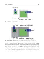
Fig. 1. An early design schematic for top-emitting and bottom-emitting VCSELs presented
by Jewell et. al. in 1989.
Following is a concise analysis of these shortcomings. We would present the basic VCSEL
structure that would try to achieve the above given objectives. Following this discussion we
would present the drawbacks in the device performance related to the realization of design
objectives. Certain remedies and improvements would then be presented in order to render
the device more performing and efficient.
2.2 VCSEL structure
A VCSEL is essentially a gain medium based active region vertically stacked between two
Distributed Bragg Reflectors (DBRs). In order to achieve a single mode operation it is
proposed that the length of the active region be very small: Effectively of the order of the
desired lasing wavelength. A short cavity eliminates the generation of longitudinal modes
associated to Fabry-Pérot cavities. This however imposes a severe restriction on VCSEL DBR
design.
The threshold gains for the surface-emitting and edge-emitting devices must be comparable
regardless of the cavity length. The threshold gain of an EEL is approximately 100cm
−1
. For
a VCSEL of active layer thickness of 0.1 μm, this value corresponds to a single-pass gain of
about 1%. Thus for a VCSEL to lase with a threshold current density comparable to that of
an EEL, the mirror reflectivities must be greater than 99% in order to ensure that the
available gain exceeds the cavity losses during a single-pass.
Achieving a reflectivity of 99% with DBRs is a formidable task and thus central to the
conception of low threshold VCSELs is the capacity to fabricate high reflectivity mirrors.
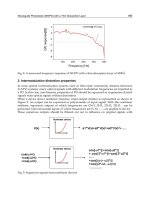
Let’s consider the example of a VCSEL operating at 850nm. The active region would consist
of several ultra thin layers composed alternately of GaAs and AlGaAs materials. The
Advances in Optical and Photonic Devices
70
difference between the refractive index of layers of a pair determines the number of pairs
required to achieve a reflectivity of 99% or more. In the case of AlAs-Al
0.1
Ga
0.9
As the
refractive index difference between two alternate layers is 0.6 as is shown in fig. 2 (Adachi,
1985). Consequently only 12 pairs are needed to achieve a reflectivity of 99% or more. As far
as AlAs and Al
x
Ga
1−x
As alloys go, the situation is conducive, even desirable, for the
fabrication of VCSELs using these materials. The band gap energy of AlAs−Al
x
Ga
1−x
As
alloys is about 1.5eV which eventually corresponds to a wavelength in the 800-900nm
region.
Fabrication technology for VCSELs emitting in this wavelength band therefore has perfectly
been mastered since monolithic growth of 12-15 DBR pairs does not pose serious fabrication
challenges. Furthermore AlAs-GaAs alloy DBRs have an excellent thermal conductivity
which allows the dissipation of heat fairly rapidly and avoids device heating which
eventually could have been responsible for VCSEL underperformance.
2.3 Performance drawbacks
As far as the fabrication of near infrared VCSELs was concerned, the existing technologies
and fabrication processes proved to be quite adequate. However, applying a similar
methodology to telecommunication wavelength VCSELs proved to be much more
challenging. Long wavelength VCSELs operating in the 1.1μm- 1.6μm range are of
considerable interest for optical fibre telecommunications since the hydroxyl absorption and
pulse dispersion nulls for silicon optical fibres are found at 1.5μm and 1.3μm respectively.
Although several material systems were considered, the combination InGaAsP-InP turned
out to be the most suitable in view of the near perfect lattice match. The active layer is
composed of the In
1−x
Ga
x
As
y
P
1−y
quaternary alloy. By varying mole fractions x and y, almost
any wavelength within the 1.1−1.6μm can be selected.
(a) Refractive Index of AlAs (b) Refractive Index of Al
0.1
Ga
0.9
As
Fig. 2. Refractive indices of AlAs and Al
0.1
Ga
0.9
As as a function operating wavelengths.
2.4 DBR growth
Only 12−15 AlAs−Al
x
Ga
1−x
As pairs are needed to fabricate a DBR with a 99% reflectivity. By
contrast, the refractive index difference between an InP- InGaAsP pair is only 0.3 and hence
more than 40 pairs would be needed to achieve a reflectivity of 99%. The problem
Optical Injection-Locking of VCSELs
71
consequently encountered concerns thermal properties of InP−based materials that
intervene to affect the process in following ways (Shau et al., 2004), (Piprek, 2003):
• For the fabrication of long wavelength VCSELs, there are mainly In
1−x
Ga
x
As
y
P
1−y
alloys
available which have to be grown on InP substrates. Due to the effects of non negligible
Auger’s recombination effects and intra-valence band absorption, these materials suffer
from temperature-dependent losses.
• The thermal conductivity is greatly reduced due to alloy disorders which causes
phonon scattering. This reduction in thermal conductivity is particularly adverse for
effective heat sinking through the VCSELs’ DBRs usually having a thickness of several
μms.
• AlAs-Al
x
Ga
1−x
As DBRs have a good thermal conductivity and could be thinner but due
to lattice mismatch could not be grown on the InP substrate.
DBR growth has been one of the fundamental problems regarding the fabrication of long
wavelength VCSELs that has hampered the entry of VCSELs in high-speed data, command
and telecommunications domain.
2.5 Optical and electrical confinement
Growing stacks of DBRs was not the only problem encountered by VCSEL manufacturers.
One of the primary objectives of VCSEL design was to fabricate short cavity single mode
devices. The short cavity did eliminate the undesirable longitudinal modes but it gave birth
to another unforeseen problem. Initial VCSEL designs suggested that the carriers and the
photons share a common path traversing the DBRs. This led to the heating of certain zones
of the DBRs due to carrier flow and resulted in a variable refractive index distribution inside
the VCSEL optical cavity. This phenomenon is known as “Thermal Lensing”. Instead of
being concentrated in the centre in the form of a single transverse mode, the optical energy
is repartitioned azimuthally inside the optical cavity. This particular optical energy
distribution is observed in the form of transverse modes. Higher bias currents therefore
imply high optical power and in consequence a higher number of transverse modes.
An oxide-aperture is employed, principally in shorter wavelength emission VCSELs, in
order to block the unwanted transverse modes. The oxide-aperture diameter then
determines the multimode or single mode character of a VCSEL. VCSELs having oxide
aperture diameter greater than 5μm exhibit multimode behaviour. It can also be inferred
from the above discussion that for the type of VCSELs employing the oxide-aperture
technology for optical confinement, single mode VCSELs almost always have emission
powers less than those of multimode VCSELs.
The problems of optical and electrical confinement are hence interrelated. It is evident that
in order to attain single mode emission the thermal lens effect must be avoided. This can
only be achieved by segregating the carrier and photon paths. Although challenging
technically, it can be achieved using a tunnel junction. The concept and functioning of a
tunnel junction is explained in the following sub-section.
2.6 The tunnel junction
The “Tunnel Junction” was discovered by L. Esaki in 1951 (Esaki, 1974) and the tunnel
junction diodes used to be labeled “Esaki Diodes” for quite some time after this discovery
(Batdorf et al., 1960), (Burrus, 1962). Esaki observed the tunnel junction functioning while
working on Ge layers but soon after his discovery, tunnel junction diodes were presented by
Advances in Optical and Photonic Devices
72
other researchers on other semiconductor materials such as GaAs, InSb, Si and InP. The
tunnel junction is formed by joining two highly doped (degenerate) “p” and “n” layers. It
has a particular current-voltage characteristic curve. A negative differential resistance region
(− dI/dV) over part of the forward characteristics can be observed.
In the case of a VCSEL the tunnel junction serves a “Hole Generator”. Under the tunnel effect,
the electrons move from valence band (doped p++) to conduction band (doped n++), leaving
holes in their place. Fig.1.12 shows the schematic diagram of a tunnel diode in reverse bias
conditions. The existence of a tunnel junction in a VCSEL presents following advantages:
• It reduces the intra valence band absorption due to P doping.
• It serves to reduce the threshold current, by improving the carrier mobility.
• It is used for electrical as well as optical confinement.
Due to these properties, the tunnel junction has become an integral part of long wavelength
VCSELs.
2.7 Technological breakthroughs and advances in long wavelength VCSEL fabrication
Although by the start of the 21st century serial production and delivery of VCSELs was in
full flow for diverse applications, they had failed to fulfil the two following essential criteria
for utilization in optical networks.
• They did not emit in the 1.3μm and 1.5μm range: The so-called “Telecoms
Wavelengths”. This meant not only definition and standardization of new standards at
850nm wavelength but also the deployment and manufacturing of a host of optical
components such as optical fibres, couplers, multiplexers and photodiodes compatible
with the 850nm emission range.
• As has been explained above, transverse-mode operation starts to manifest itself from a
few milli-amperes above the threshold current rendering the VCSELs multimode in
character. This multimodality is disconcerting in two ways:
- It reduces the effective channel bandwidth hence reducing the maximum deliverable bit
rate.
- It requires the utilization of multimode optical fibre which although being less
expensive than the single mode fibre, affects the VCSEL operation in another way.
When high optical powers are injected in a multimode fibre, several undesired fibre
modes are excited thus reducing the effective bandwidth.
It is clear from the above discussion that a suitable substitute for EELs, for applications in
short to medium distance optical fibre networks, must possess the following properties:
• It must emit at either 1.3μm or at 1.5μm wavelength so that the existing standards,
infrastructure, optoelectronic components and devices could be utilized.
• It must have a single mode emission spectrum so as to profit from the high bandwidths
offered by the employment of single mode optical fibres.
As late as 2000, there were no serial production and mass deployment of VCSELs that
fulfilled these two essential criteria. As has been discussed above, this was due to the
technical challenges posed by a combination of several different factors which rendered the
fabrication of long wavelength VCSEL devices very difficult.
2.8 Emergence of long wavelength VCSELs
Regarding the manufacturing of long wavelength VCSELs, several different research groups
kept trying to realize long wavelength emission devices. In 1993, Iga et al. demonstrated the
Optical Injection-Locking of VCSELs
73
CW operation of a 1.3μm InGaAs-InP based VCSEL at 77K (Soda, 1979). The upper DBR
consisted of 8.5 pairs of p-doped MgO-Si material with Au-Ni- Au layers at the top while
the bottom DBR consisted of 6 pairs of n-doped SiO-Si material (Dielectric Mirror). In 1997,
Salet et.al demonstrated the pulsed room-temperature operation of a single mode InGaAs-
InP VCSEL emitting at 1277nm. The bottom mirror consisted of n-doped InGaAsP-InP
material grown epitaxially to form a 50 pair DBR mirror with a 99.5% reflectivity (Salet et al.,
1997).
Fig. 3. A long wavelength VCSEL with a tunnel junction emitting at 1.55μm presented by
Boucart et. al in 1999.
The device threshold current at 300K was 500mA. The top mirror was realized using p-
doped SiO
2
-Si reflectors. A year later, in 1998, Dias et al. reported the growth of InGaAsP-
InP, AlGaInAs-AlInAs and AlGaAsSb-AlAsSb based DBRs on InP substrates to achieve
reflectivities up to 99.5% (Dias et al., 1998). Soon afterward, in 1999, Boucart et al extended
their previous work to demonstrate the room temperature CW operation of a 1.55μm
VCSEL. In this case the top DBRs consist of 26.5 n-doped GaAs-AlAs pairs which were
grown directly on an n-InP substrate (Metamorphic mirrors). A tunnel junction was
fabricated to localize the current injection. The bottom mirror consisted of 50 pairs of n-
doped InGaAsP-InP layers having a reflectivity of 99.7%. The device had a threshold current
of only 11mA and had been fabricated using gas-based Molecular Beam Epitaxy (MBE)
(Boucart et al., 1999).
The tunnel junction proved benificial in two ways:
• It enabled the utilization of two n-doped DBRs;
• Once the conductive properties of the tunnel junction were neutralized using H+ ion
implantation, it served to localize the current injection without having to etch a mesa.
Advances in Optical and Photonic Devices
74
The resulting device was therefore coplanar in structure. It can be ascertained from Table.1.1
that several different materials such as InGaAsP, InGaAsAl, InGaAsSb and InGaAsN were
chosen to fabricate the active layer. The material choice for DBRs and the fabrication
processes were equally diverse. Although most of the research groups chose “Monolithic
Integration Techniques” for the fabrication of VCSELs, “Wafer Fusion”, and “Fusion
Bonding” were also applied.
Meanwhile, in 1998, the Institute of Electrical and Electronics Engineers (IEEE) defined the
“1000BASEX-Gbps Ethernet over Fibre-Optic at 1Gbit/s” standard. This standard for the
transmission of “Ethernet Frames” at a rate of at least one Gbps was defined using light
sources emitting at 850nm. The definition of Gigabit Ethernet standards using 850nm optical
sources boosted the research and development of near infrared emission VCSELs. By the
year 2000, 850nm VCSELs had firmly established themselves as standard optical sources for
short-haul communication applications. This development was a setback for ongoing
research in long wavelength VCSELs and as a result many research groups shifted their
focus from long wavelength VCSEL development to other emerging fields. Furthermore, the
research focus, even in the long wavelength VCSEL development field, shifted toward a
new dimension. Long wavelength VCSELs were no longer being developed solely as
telecommunication sources, an emerging field of spectroscopy was beginning to play an
increasingly important part in eventual long wavelength VCSEL applications.
2.9 Vertilas VCSELs
Fig. 4. A Vertilas BTJ structure with an emission wavelength of 1.55μm [28].
Although long wavelength VCSEL operation using a tunnel junction device was already
demonstrated by Boucart et al. in 1999, Ortsiefer et al. presented a variation to this concept.
Soon the single mode room temperature operation of an InP-based VCSEL operating at
1.5μm was demonstrated by the same research group (Ortsiefer et al., 1999), (Ortsiefer et al.,
2000). The top DBR is composed of 34.5 InGaAlAs-InAlAs pairs. The bottom mirror is
comprised of 2.5 pairs of CaF2-Si with Au-coating. The gold coating, apart from serving as a
Optical Injection-Locking of VCSELs
75
high reflectivity mirror (99.75%), serves as an integrated heat sink (Shau et al., 2004). The
successful incorporation of tunnel junction in the long wavelength VCSEL design proved to
be the technical breakthrough that would present VCSELs as standard devices for short to
medium distance optical fibre communications. By 2002 Vertilas was delivering 1.55μm
single mode VCSELs for 10Gbps operation.
2.10 BeamExpress VCSELs
The manufacturing of a long wavelength VCSEL requires the growth of an InP-InGaAsP
alloy active region on an InP substrate. These alloys however are difficult to grow as DBR
stacks above and below the active region since the restrictions imposed by the material
thermal conductivity render proper device functioning impossible. On the other hand,
AlAs-Al
x
Ga
1−x
As DBRs have a good thermal conductivity but they can not be monolithically
grown on InP-based substrates due to lattice mismatch. The solution to the matching of
disparate materials to optimize VCSEL performance was developed at the University of
California Santa Barbara (UCSB) in 1996 by Margalit et al. (Margalit et al., 1996). The
technique utilized is known as “Wafer Fusion” or “Wafer Bonding” and consists of
establishing chemical bonds directly between two materials at their hetero-interface in the
absence of an intermediate layer (Black et al., 1997). The first demonstration constituted of
fabrication of a 1.55μm VCSEL. The device was fabricated by wafer fusion of MOVPE-
grown InGaAsP quantum well active region to two MBEgrown AlGaAs-GaAs DBR
reflectors (Margalit et al., 1996).
By applying a variant of the “Wafer Fusion” technique in 2004, Kapon et. al demonstrated
that it was possible to grow separate components of a VCSEL cavity on separate host
substrates (Syrbu et. al, 2004), (Syrbu et. al, 2005). These separate components were then
bonded (fused) together to construct the complete VCSEL optical cavity. This process was
developed at the Ecole Polytechnique Fédérale de Lausanne (EPFL) and patented as
“Localized Wafer Fusion”. Fig. 5 presents the structure of a BeamExpress VCSEL with an
emission wavelength of 1.55μm. This is a double intracavity contact single-mode VCSEL
with coplanar access. The InP-based optical cavity consists of five InAlGaAs quantum wells.
The top and bottom DBRs comprise of 21 and 35 pairs respectively and are grown by Metal-
Organic Chemical Vapor Deposition (MOCVD) epitaxy method. Using the technique of
localized wafer fusion, the top and the bottom AlGaAs-GaAs DBRs are then bonded to the
active cavity wafer and the tunnel junction mesa structures. Using VCSELs with double
intracavity contacts has its own advantages. These contacts are much nearer to the active
region than the classical contacts. Their utilization combined with the presence of tunnel
junction allows having lower series resistance as compared to oxidized-aperture VCSELs. Due
to this proximity of the contacts to the active region these VCSELs tend to have high quantum
efficiency. Their location near the active region results in no current passage through DBRs.
The process used for the fabrication of Beam Express VCSELs is not monolithic. The bottom
AlGaAs-GaAs DBR is grown on the GaAs substrate. The InP-based cavity is then bonded to
this DBR. After the growth of an isolation layer on the active region, the epitaxially grown
AlGaAs-GaAs top DBR is fused to complete the optical cavity. This double fusion increases
the complexity of the fabrication process but it presents certain advantages. Waferfusion
allows replacing the InAlGaAs DBRs by GaAs DBRs. Not only the GaAs DBRs have a better
thermal conductivity, they are much cheaper than InAlGaAs DBRs which allows increasing
the performance and decreasing the cost of the component at the same time. The biggest
Advances in Optical and Photonic Devices
76
advantage of “Wafer Fusion” is the possibility of serial production of VCSELs which further
serves to reduce the component cost.
Fig. 5. Schematic diagram of a wafer-fused Beam-Express VCSEL with an emission
wavelength of 1.5μm.
2.11 RayCan VCSELs
Starting as a spin-off company from the Korean government funded Electronics and
Telecommunications Research Institute (ETRI) in 2002, RayCan launched an ambitious
project for manufacturing of long wavelength VCSELs. Instead of using the above described
specialized technologies for long wavelength VCSEL manufacturing, RayCan decided to
embark upon a different course. They decided to monolithically grow InAlGaAs DBRs and
an InGaAs-based quantum well active region on an InP substrate. As has been discussed
above, this technique was previously not considered because in order to achieve 99%
reflectivity using InAlGaAsbased DBRs, a growth of more than 40 pairs is needed. RayCan
employed Metal-Organic Chemical Vapour Deposition (MOCVD) technique to fabricate a
long wavelength VCSEL.
For 1.55μm VCSELs, the top and bottom DBRs were grown as 28 and 38 pairs of un-doped
InAlGaAs-InAlAs schemes. The top and bottom DBRs consisted of 33 and 50 layers
respectively for 1.3μm emission VCSELs. The 0.5
λ
thick active region consists of seven pairs
of strain-compensated (SC) InAlGaAs quantum wells (Park et al., 2006). The lower number
of top DBRs in both the VCSELs was compensated by using an InAlGaAs phasematching
layer and Au metal layer. Fig. 6 presents the structure of a RayCan VCSEL emitting at
1.5μm. RayCan has been shipping 1.3μm and 1.5μm VCSELs since 2004. In November 2005
RayCan shipped its first 10GBit/s long wavelength CWDM VCSEL module.
2.12 Long wavelength VCSEL direct modulation
Up to this point we have discussed the prospects of long wavelength VCSELs in the context
of high bit rate data delivery over medium and short distance links. It would not be an
exaggeration to state that consumer demand for multimedia and interactive applications
and therefore bandwidth has increased to an unprecedented level. Current electrical-
electrical infrastructures can not support this demand. The major obstacle in switching from
Optical Injection-Locking of VCSELs
77
electrical/ hertzian systems to optical/fibred systems is the cost of the coherent optical
source compatible with existing infrastructure. Recent advances in the fabrication,
development and serial production of VCSELs emitting at 1.3μm and 1.5μm have paved the
way for future FTTX systems.
Having been able to solve the problem at component level, by developing reliable long
wavelength VCSELs, the next logical approach is the development of new systems
incorporating these components. Conventionally the EELs used in the long-haul fibre links
are externally modulated i.e. the photon generation process inside the cavity is independent
of the modulation mechanism. While being extremely effective, this method necessitates the
utilization of an external modulator which increases the system cost. Such a scheme is
inherently unfeasible for FTTX systems due to the cost of the external modulators. The
elimination of external modulators as a component of choice for FTTX systems decrees the
employment of direct modulation techniques. In this technique the laser diode bias current
is varied to achieve the optical output intensity variation. Apparently the scheme is simple
and easy to implement, but when put into practice, it presents two major problems which
are detailed in the following two sub-sections.
2.13 Phase-amplitude coupling
Semiconductor lasers, whether EELs or VCSELs, are different from other lasers in one
respect. The refractive index of a semiconductor laser depends on the carrier concentration
inside the cavity. The carrier concentration variation affects the refractive index of the cavity
which eventually changes the emission wavelength of the component. The consequences of
this uniqueness manifest themselves during the process of direct modulation. A variation in
bias currents varies the optical output power as well as the optical frequency of the cavity.
These variations are proportional to the variation in carrier concentration and therefore the
bias current.
Fig. 6. MOVCD Grown monolithic structure of a 1.5μm RayCan VCSEL.
Advances in Optical and Photonic Devices
78
The device is modulated in amplitude and frequency at the same time. This phenomenon of
“Phase-Amplitude Coupling” or the dynamic shift of the lasing frequency during
modulation is known as “Frequency Chirping” or simply “Chirping”.
Chirping broadens the linewidth of a laser. The extent to which a pulse broadens depends
upon the amplitude of the modulating signal. Larger modulation amplitudes result in
linewidths of the order of GHz 1. This spectral broadening at the time of modulation
becomes more pronounced during the passage of the modulated pulse through an optical
channel and the effective channel bandwidth is reduced. Direct modulation while being
costeffective proves to be inefficient, in terms of deliverable bit rates, when compared to
external modulation.
2.14 Intrinsic modulation limits
A semiconductor optical cavity, in essence, is a resonator. Like every resonator, or electrical
circuit for that matter, its frequency response depends on its intrinsic parameters. In case of
semiconductor lasers these parameters might be cavity volume, photon and electron
populations, group velocity, gain compression factor etc. When directly modulated, a laser
can not better the modulation frequency response already defined by these intrinsic
parameters. On the other hand, the utilization of an external modulator provides a means to
bypass the laser intrinsic parameters. The modulation response (or the deliverable bit rate)
of the system is then defined by the external modulator and not the laser.
2.15 Long wavelength VCSEL optical injection-locking
It is clear from the description of the two above given problems that a viable optical system
must minimize the effects of “Amplitude-Phase Coupling” and “Intrinsic Modulation
Limits” in order to be efficient and acceptable. Once injection-locked, the master laser holds
the frequency of the follower laser and makes it immune to carrier variations. This isolation
from carrier variations appears as the reduction of chirp during direct modulation. In 1984,
Lin et al. demonstrated the reduction of frequency chirping in a directly modulated
semiconductor laser by the application of injection-locking technique (Lin et al., 1984).
Henry presented an approximate formula for the calculation of resonance frequency of
optically injection-locked semiconductor lasers (Henry et al., 1985) but its significance was
not appreciated at that time until Simpson and Meng demonstrated bandwidth and
resonance frequency enhancements in late 90’s (Simpson et al., 1996), (Meng et al., 1998). In
2002, a research group in University of California Berkley (UCB), led by Connie J. Chang-
Hasnain reported the first optical injection-locking of a long wavelength VCSEL for 2.5Gbps
transmission (Chang et al., 2002).
In 2003 long wavelength VCSEL chirp reduction and bandwidth enhancement were
presented by the same research group (Chang et al., 2003) but there was a marked technical
difference from their first publication. Whereas the first time optical injection-locking of a
long wavelength VCSEL was carried-out using an identical VCSEL, the second
demonstration used a Distributed FeedBack (DFB) laser to injection-lock a long wavelength
VCSEL. The group has extensively published on the subject of the optical injection-locking
of long wavelength VCSELs, but this pattern of locking a VCSEL with a DFB has remained
unchanged since.
Several optical injection-locking studies regarding semiconductor lasers have reported
frequency-chirp reduction (Lin et al., 1984), (Sung et al., 2004) increased RF link gain
Optical Injection-Locking of VCSELs
79
(Chrostowski et al. 2003), (Chrostowski et al. 2007), improved relative intensity noise (Yabre
et al., 2000) and diminished non-linear distortion (Chrostowski et al. 2007). Although the
utilization of a DFB laser to injection-lock a VCSEL is excellent for demonstration of
phenomena related to optical injection-locking, its practical application presents two major
drawbacks. Without immediately entering into the details of these drawbacks, it can be
logically inferred that both these drawbacks are related to the utilization of the DFB laser.
First of all the physical symmetry of the two lasers used is not the same. The VCSELs are a
vertical emission device while the DFB lasers emit in the horizontal direction. This
asymmetry renders the integration of an optical injection-locking system consisting of a DFB
laser and a VCSEL very difficult. The second reason, of course, is the cost. One of the
reasons of employing VCSELs in optical networks for high-speed data communication is
their cost-effectiveness. Utilization of a DFB laser to improve the transmission and the
component characteristics compromises this very objective. Due to these reasons despite all
these advances regarding this very potent combination of semiconductor lasers and optical
injection-locking, the phenomenon and its practical applications have not got any
commercial breakthrough as yet.
With the arrival of Vertical-Cavity Surface-Emitting Lasers (VCSELs) on the commercial
scene as low-cost, integrable sources, the efforts to revive the optical injection-locking
phenomena were once again undertaken and follower VCSEL resonance frequencies
ranging from 27 Ghz to 107 GHz have been reported in recent years (Chrostowski et al.
2007). The problem of non-integrability however is still unresolved due to the utilization of a
distributed feedback (DFB) laser as master optical source to injection-lock a follower VCSEL.
The DFB lasers have horizontal optical cavities. This physical asymmetry renders the
monolithic integration very complicated. On the other hand the utilization of a powerful
DFB laser compromises the economy of the setup by increasing the cost dramatically and
fails the purpose of using a VCSEL in the first place. Clearly the solution to afore-mentioned
problems would be to try a VCSEL-by-VCSEL optical injection-locking approach.
3. VCSEL rate equations
The previous chapter introduced the overall historical background of the subject and the
motivation for undertaking this research work. In this chapter we will present a complete
theoretical analysis of the optical injection-locking phenomenon in semiconductor lasers. A
semiconductor laser cavity is essentially a resonator and its input (electrons) and output
(photons) can be demonstrated to be interrelated to each other via cavity parameters. Like
any other resonator cavity, the quality factor “Q” and the resonance frequency of this cavity
can be controlled by manipulating its physical dimensions or intrinsic parameters.
Ordinarily, the only externally manipulable variable is the electron concentration that can be
varied by changing the bias current. During the optical injection-locking process the internal
parameters of the cavity are changed by varying the photon concentration inside the cavity.
Since the locking effect is the result of interaction between two optical fields, the phase
difference between the master and follower VCSELs can also be varied to achieve the
desired effect.
Ordinarily, the only externally manipulable variable is the electron concentration that can be
varied by changing the bias current. During the optical injection-locking process the internal
parameters of the cavity are changed by varying the photon concentration inside the cavity.
Since the locking effect is the result of interaction between two optical fields, the phase
Advances in Optical and Photonic Devices
80
difference between the master and follower VCSELs can also be varied to achieve the
desired effect.
(1)
(2)
Where N(t) and S(t) are the electron and photon densities,
η
i
the internal quantum
efficiency, q the electron charge, V
act
the active region volume, v
g
the group velocity,
β
the
spontaneous emission coefficient, Γ the confinement factor and
τ
P
the photon lifetime.
The spontaneous emission rate, R
sp
is defined in terms of the constants A, B and C where A
represents the Shockly-Read-Hall non-radiative recombination coefficient, B the bimolecular
recombination coefficient and C the Auger non-radiative recombination coefficient. The gain
G can be expressed as
(3)
Where N
tr
is the transparency carrier density, a
0
the differential gain coefficient and
ε
the
gain compression factor.
A third equation describing the phase behaviour of the device can be introduced as follows:
(4)
α
H
is the “Phase-Amplitude” coupling factor and is referred to as “Henry’s Factor”. It might
be important to note here that equation 2.4 is not a coupled equation i.e. the term does not
appear in equations 2.1 and 2.2. Lang proposed the utilization of three equations, instead of
two, to model an optically injection-locked system (Lang, 1982). Lang’s equations coupled
the electric field variations in the cavity directly to carrier and phase variations and as such
rendered the physical interpretation of the phenomenon somewhat cumbersome. In 1985, P.
Gallion et al. presented the optical injection-locking rate equations that replaced cavity
electrical field by photon number (Gallion & Debarge, 1985), (Gallion et al., 1985). Following
the injection of optical power in the optical cavity, the dynamics of the follower laser
change. This change can be mathematically presented by modifying the VCSEL rate
equations to compensate for optical injection.
(5)
(6)
(7)
Optical Injection-Locking of VCSELs
81
It must be remarked that while the equation concerning the carrier density remains
unchanged, the equations regarding the phase and the photon density are modified to
accommodate for the effects of external light injection.
Two very important parameters of note, S
inj
and
θ
are added to equations 2.6 and 2.7. S
inj
represents the photon density injected inside the follower VCSEL optical cavity while
θ
denotes the phase difference between the master and follower optical fields so that:
(8)
(9)
Apart from frequency detuning, phase difference and injected optical power, the fourth
parameter which characterizes an optically injection-locked system is the “coupling
coefficient” of a laser. It is defined as k
c
and can be expressed mathematically as
(10)
This coefficient describes the rate at which the injected electric field adds to the follower
cavity electric field as a function of the VCSEL optical cavity length. ‘L’ is the length of the
VCSEL optical cavity.
2.2 Locking Range Calculations
Solving equations (5) and (6) in the steady-state regime which renders
and
equal to
zero gives the very important parametric equation:
(11)
The dependence of equation (11) on
α
H
can be elaborated by using the linear combination
property for sinuses and cosines. Using this property we can write that:
(12)
This relation is important because it helps the calculation of effective locking bandwidth of
an injection-locked system. Moreover it can be deduced that due to the presence of the sine
function, the inequality is limited to the range of:
(13)
On the other hand, it appears that the oscillation limit for
θ
is between -
π
/2 and
π
/2. Δ
ω
is
then bounded by:
(14)
The asymmetry of the locking range can be explained both mathematically and physically.
Mathematically speaking, if we observe (14), we can see that due to the multiplication with
the term
α
H
on the left hand side, this relation becomes asymmetric with respect to
α
H
.
Advances in Optical and Photonic Devices
82
Fig. 7. 2D presentation of calculated locking range of a long wavelength VCSEL with
α
H
= 3
showing the locking-range dependence on injected optical power.
Physically speaking, during the injection-locking of a semiconductor laser the increased
photon population changes the refractive index and leads to a cavity wavelength shift in the
longer wavelength direction and finally an asymmetric locking range. Calculated locking-
range for
α
H
=3 is presented in fig. 7. It can be observed from equation (14) that a higher
value of
α
H
leads to higher locking-range: A higher value of
α
H
favours locking in the
negative frequency detuning range. In terms of locking-range characteristics, VCSELs are
different from EELs. Locking range determines the extent of frequency enhancement of an
optically injection-locked laser. Equation (14) shows that the locking-range depends on
injected power and coupling coefficient k
c
. Therefore mathematically it can be stated that the
locking-range follows the variation of the term
Since a VCSEL cavity is much shorter than an EEL cavity, VCSELs have typically very high
values of k
c
(10) as compared to those of conventional lasers. This implies that VCSEL
locking-ranges are higher compared to EEL locking-ranges and can potentially lead to much
higher resonance frequencies.
3.1 Small signal analysis
We begin by presenting once again the “Modified VCSEL Rate Equations”. The small signal
analysis is performed to derive the S
21
response of an injection-locked VCSEL. Consider that
a sinusoidal signal modulates a laser biased at current I. The resulting expression for current
I then becomes:
(15)
Optical Injection-Locking of VCSELs
83
Similarly, the carrier, photon and phase variations can be described as follows:
(16)
(17)
(18)
By putting
(19)
(20)
(21)
We have:
(22)
(23)
(24)
The gain, as defined in (3), contains both the carrier and the photon terms. Partial
differentiation of (3), with respect to the carrier and photon densities N and S, yields two
new variables G
N
and G
S
, where G
N
and G
S
are defined as:
(25)
(26)
Differentiating equation (5) with respect to N, S and
φ
therefore results in the following set
of three equations:
(27)
(28)
(29)
Advances in Optical and Photonic Devices
84
Similarly if we define a new variable
ρ
as:
(30)
And differentiate equation (6) with respect to N, S and
φ
we have the following set of
equations:
(31)
(32)
(33)
The partial differentiation of the phase equation (7) with respect to N, S and
φ
results in the
following set of equations:
(34)
(35)
(36)
Linearised rate equations can then be expressed as:
(37)
(38)
(39)
Replacing the partial derivatives by intermediate variables gives
(40)
(41)
(42)
Optical Injection-Locking of VCSELs
85
This can be readily arranged into a three equation matrix system as follows:
(43)
Taking the Laplace transform of the equation set in order to pass from time-domain to
frequency-domain, and arranging, yields:
(44)
In order to solve this three-equation matrix system we have to calculate the determinant of
the intermediate variable matrix:
(45)
Where
(46)
Using the Kramer’s rule, the photon density variation can be expressed as:
(47)
Simplifying equation 1.55 leads to:
(48)
(6) and (7) can alternatively be solved to obtain a relation in terms of the phase difference
between two lasers and is presented below:
(49)
Advances in Optical and Photonic Devices
86
3.2 Numerical simulations
The mathematical model proposed above is implemented in MATLAB in order to observe
the small-signal response of an injection-locked system. Table 1 summarises the VCSEL
intrinsic parameters used to calculate the S
21
response of an injection locked system (Bacou,
2008).
3.3 Simulation results
Recently the most significant application of optical injection-locking has been in the domain
of resonance frequency enhancement. The enhanced resonance frequency can lead to an
extended bandwidth many times the original device bandwidth. The modulation response
of an injection-locked laser can be characterized as one of the following three:
• High Resonance Frequency, Low Bandwidth
• High Resonance Frequency, High Bandwidth
• Low Resonance Frequency, Low Bandwidth
Although the resonance frequency of an optically injection-locked laser increases with
increasing injected power levels, the frequency detuning between the two lasers plays a very
important role in determining the eventual characteristics of the S
21
curve and finally the
effective bandwidth. The above presented three different kinds of modulation responses
depend on different locking conditions and parameters and are described in the following
section.
3.4 High resonance frequency, low bandwidth
The high resonance frequency, low bandwidth operation regime can be attributed to a
positive frequency detuning. Since the resonance frequency of an injection-locked system is
the difference between the master laser frequency and the down shifted follower cavity
frequency, positive frequency detuning results in very high resonance frequencies.
Table 1. Long wavelength VCSEL intrinsic parameters used to simulate the small-signal
injection-locking behaviour (Bacou, 2008).
Optical Injection-Locking of VCSELs
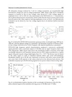
87
Fig. 8. Calculated S
21
response of an optically injection-locked VCSEL with constant injected
power and variable positive frequency detuning. The detuning is varied from 10 GHz to 110
GHz.
On the other hand, optically injection-locked systems can be mathematically defined as
third-order systems and suffer from low-frequency dips due to the presence of a parasitic
pole. Fig. 8 presents the simulated S
21
response of an optically injection-locked VCSEL
operating in the positive frequency detuning regime. The injected optical power is
maintained constant for this set of curves in order to study the effects of variation in positive
frequency detuning. The resonance frequency increases with increasing difference between
the master and follower VCSEL frequencies.
Although from a telecommunication point of view, enhancement in resonance frequency is
desired but the low frequency dip of an optically injection-locked system operating in the
positive frequency detuning regime limits the effective bandwidth of the system and
renders the system inefficient. This configuration therefore is not desired for operation in
Datacom and telecommunication environments.
Very high resonance frequencies however can be beneficial for another very important
application i.e. the generation of millimetre-wave signals. Since the proposal of the 60GHz
band for the radio link frequency in broad-band cellular systems, the utilization of optical
fibre for signal distribution has attracted much interest. This is due to low-loss nature of the
optical fibres that are capable of transmitting data at very high bit rates. The main obstacle
in the implementation of this scheme is the conception of a high frequency oscillator.
Goldberg et. al had already demonstrated the generation of microwave signals using
Advances in Optical and Photonic Devices
88
injection-locked laser diodes in 1983 [16], but the enthusiasm in the implementation of this
scheme faded away due to the incipient nature of semiconductor lasers at that time.
3.5 High resonance frequency, high bandwidth
Positive frequency detuning can be employed to achieve very high resonance frequencies
that could be useful for certain applications such as microwave and millimetre-wave signal
generation but such high resonance frequencies imply very low cut-off frequencies due to
low-frequency dip associated to positive frequency detuning. This situation can be
improved by operating the laser at close to zero detuning. In such a configuration, the cut-
off frequency increases with increase in injected power but due to very low frequency
detuning value there is no loss at low frequency values. Frequency detuning has little or no
effect on the resonance frequency of such a system and the bandwidth increase is dependent
only on optical injected power. This configuration can be employed for broadband digital
communications that require the transmission of very high bit rates. The third operation
regime is defined by negative frequency detuning. Fig. 2.10 presents a set of simulated S
21
curves with increasing negative frequency detuning. It is clear from Fig. 2.10 that for
positive frequency detuning values, the follower VCSEL S
21
response is un-damped with
high resonance frequencies. However when the detuning between the two VCSELs is varied
in the negative detuning operation regime, the S
21
response curves start to become highly
damped.
Fig. 9. Simulated S
21
response of an optically injection-locked follower VCSEL showing cut-
off frequency enhancement.
3.6 Low resonance frequency, low bandwidth
At the same time, the low frequency dip, exhibited due to positive frequency detuning
operation regime starts to disappear. Finally at relatively high values of negative frequency
detuning the S
21
curves become over-damped and gradually the resonance peak vanishes.
Optical Injection-Locking of VCSELs
89
Fig. 10. Calculated S
21
response of an optically injection-locked VCSEL with constant injected
power and variable negative detuning. The detuning is varied from 10 GHz to -190 GHz.
The negative frequency detuning can hence be used to generate high low frequency gain S
21
curves. This is particularly important for directly modulated optical fibre links. The losses in
such links, apart from coupling and connector losses, are due to Electrical- Optical (E/O)
and Optical-Electrical (O/E) conversion. Sung et al. have demonstrated that by injection-
locking a laser in negative frequency detuning regime the RF link gain can be improved by
up to 10 dB [21].
3.7 Comparison between free-running and injection-locked VCSEL models
Fig. 11 presents a comparison between the free-running and injection-locked S
21
response of
a VCSEL. The frequency responses are plotted on a logarithmic scale in order to highlight
the difference between the respective slopes of the two systems. The injection-locked system
has a slope of -18dB/octave as compared to a slope of - 12dB/octave for a free-running
VCSEL.
Another important difference of note is the low frequency dip in the optically injection-
locked VCSEL S
21
response which is due to the extra pole in the transfer function
denominator. By putting S
inj
and Δ
ω
to zero the modified VCSEL rate equations are reduced
to classical VCSEL rate equations.
The simulations, under different operating conditions, of optically injection-locked VCSELs
presented in this chapter reveal certain interesting patterns. First of all, it must be noted that
due to the very highly selective nature of the DBR mirrors used in the VCSEL
Advances in Optical and Photonic Devices
90
manufacturing, a very small amount of light enters in the cavity. This is clear from the
locking-range calculations presented in Fig. 7. It is therefore not the injected optical power
intensity that is mainly responsible for injection-locked VCSELs’ S
21
curves variations. It is in
fact the coupling factor k
c
whose numerical value is responsible for high locking ranges,
facility of injection-locking and high resonance frequencies.
Another important point is the S
21
curve shape dependence on the frequency detuning value
between the two VCSELs. The frequency detuning is the dominant factor in determining the
shape of the S
21
curve and whether it would be high resonance frequency under-damped
response or a low resonance frequency high bandwidth flat response. This phenomenon can
be explained by understanding the beat-frequency generation effect produced inside the
follower VCSEL optical cavity.
Finally, due to optical coupling with the master laser, the dynamic response characteristics
of the follower VCSEL change. Usually a two-equation mathematical model is utilized in
VCSEL dynamic response simulations. This model gives way to a three-equation system
which incorporates the effect of external light injection. Due to this third equation, the
presence of a 3rd pole is observed in the transfer function of the optically injection-locked
VCSEL. At positive detuning frequency values, this pole becomes dominant at low
frequencies and causes the S
21
response to suffer dips of several dBs which in turn severely
limits the effective bandwidth of the system.
Fig. 11. Comparison between the free-running and injection-locked transfer functions of a
VCSEL.
The injection-locking experiments carried-out during the course of this work evolved
progressively in their complexity. The objective was to demonstrate and understand the
VCSEL-by-VCSEL optical injection-locking phenomena under different operating
constraints. Our focus was the study of variations in S
21
response of injection-locked VCSELs
under different injection powers and varying detuning frequencies.