Advances in Optical and Photonic Devices 2011 Part 6 docx
Bạn đang xem bản rút gọn của tài liệu. Xem và tải ngay bản đầy đủ của tài liệu tại đây (1.74 MB, 25 trang )
Advances in Optical and Photonic Devices
116
9. Prolonged performance of the Ce:LiCAF laser
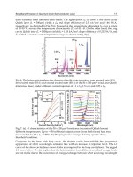
In this test, the Ce:LiCAF laser was operating continuously for 4 hours daily during 20 days.
The operating conditions were maintained constant over the duration of the test. The output
power at the pump wavelengths (527 nm, 262 nm) and of the Ce:LiCaF laser output at 290
nm was continuously monitored. The drift in the phase matching in the CLBO crystal has
been periodically revised and eliminated.
The observed variations in Ce:LiCAF output (290 nm) follows those of green pump beam
(527nm) and do not exceed 8 %. as showed at the Fig.16.
10. Conclusion
A highly efficient, compact and rugged 1 kHz tunable UV Ce:LiCAF laser pumped by the
fourth harmonic of a diode–pumped commercial Nd:YLF laser for ozone DIAL
measurements has been developed and the performance of this laser was investigated. The
Ce:LiCAF laser delivered 1 mJ pulse energy at 290 nm wavelength and was able to be
wavelength tuned from 281 to 316 nm that was achieved with a single fused silica
dispersion prism in the laser cavity. Fast shot-to-shot wavelength switching was obtained by
the harmonic motion of tuning mirror mounted on a servo-controlled high speed
galvanometric deflector.
11. References
Browell, E.V., (1991). Differential Adsorption Lidar Sensing of Ozone, Proc. IEEE, 77, pp. 419-
432, Carswell.
Fromzel, V.A., and Prasad C.R., (2003). A Tunable Narrow Linewidth 1kHz Ce:LiCAF Laser
with 46% Efficiency, OSA TOPS, Vol.83, Advanced Solid-State Photonics, pp. 203-209.
Govorkov, S.V.; Weissner, A.O., Schroder, Th., Stamm, U., Zschoke,W., and Basting, D., 1998.
“Efficient high average power and narrow spectral linewidth operation of Ce:LiCAF
laser at 1 kHz repetition rate,” Advanced Solid State Lasers, OSA TOPS 19, pp. 2-5.
McGee, T.J.; Gross, M.R., Butler, J.J., and Kimvilakani, P.E., (1995). “Improved stratospheric
ozozne lidar”, Optical Engineering, Vol. 34, pp. 1421-1430.
McDermit, S.; Walsh, T.D., Deslis, A., and White, M.L., (1995). “Optical system design for a
stratospheric lidar system,” Applied Optics, Vol. 34, pp. 6201-6210.
Mori,Y.; Kuroda, I., Nakajima, S., Sasaki, T., and Nakai, S., (1995). “New nonlinear optical
crystal: cesium lithium borate,” Appl.Phys. Lett., 67, p.1818.
Profitt, M.H., and Langford, A.O., (1977). Applied Optics, 36, No.12, pp. 2568-2585,
Richter, D.A., Browell, E.V., Butler,C.F., and Noah,S.H., (1997). “Advanced airborne UV DIAL
system for stratospheric and tropospheric ozone and aerosol measurements”, Advances in
Atmospheric Remote Sensing with Lidar, pp. 317-320, Springer, Berlin.
Stamm, U.; Zschocke, W., Schroder, T., Deutsch, N., and Basting, D., (1997). “High efficiency
UV-conversion of a 1 kHz diode-pumped Nd:YAG laser system,”in Advanced Solid
State Lasers, C.R.Pollock and W.R.Bosenberg, OSA TOPS vol.10, p. 7.
Sunersson, J.A.; Apituley, A., and Swart, D.P.J., (1994). “Differential absorption lidar system
for routine monitoring of troposperic ozone,” Applied Optics, Vol. 33, pp. 7046-705.
Taguchi, A.; Miyamoto, A.,Mori, Y., Haramura, S., Inoue, T., Nishijima, K., Kagebayashi, Y.,
Sakai, H., Yap, Y.K., and Sasaki, T., (1997). “Effects of moisture on CLBO,”in
Advanced Solid State Lasers, C.R.Pollock and W.R.Bosenberg, OSA TOPS vol.10, p.19.
Optical and Photonic Devices
7
Single Mode Operation of 1.5-μm
Waveguide Optical Isolators Based
on the Nonreciprocal-loss Phenomenon
T. Amemiya
1
and Y. Nakano
2
1
Quantum Nanoelectronics Research Center, Tokyo Institute of Technology,
2
Research Center for Advanced Science and Technology, University of Tokyo,
Japan
1. Introduction
The explosive growth of Internet traffic requires the development of advanced optical
telecommunication networks that can enable the high-speed processing of this exponentially
growing data traffic. Such advanced network systems will need an enormous number of
optical devices, so photonic integrated circuits (PICs) are indispensable for constructing the
system at low cost, reduced space, and high reliability. To date, monolithic integration on an
indium phosphide (InP) substrate is the most promising way of making PICs because it has
the capability to integrate both active and passive optical functions required in optical
transport systems for the 1.3-um or 1.55-um telecom window. To develop large-scale, InP-
based monolithic PICs, various planar optical devices such as lasers, modulators, detectors,
multiplexers/demultiplexers, and optical amplifiers have been developed [1-4].
This paper provides an overview of the present state of research on waveguide optical
isolators for InP-based monolithic PICs. Optical isolators are indispensable elements of PICs
used to interconnect different optical devices while avoiding the problems caused by
undesired reflections of light in the circuit. They must have the form of a planar waveguide
because they must be monolithically combined with other semiconductor-waveguide-based
optical devices such as lasers, amplifiers, and modulators. Conventional isolators cannot
meet this requirement because they use Faraday rotators and polarizers, which are difficult
to integrate with waveguide-based semiconductor optical devices. For this reason, many
efforts have been expended in developing waveguide isolators [5-11]. Although the research
on waveguide isolators is still in the experimental stage, it will probably reach a level of
producing practical devices in the near future.
In Section 2, we first give a short sketch of conventional optical isolators. The conventional
isolator is a mature device made with established technology and has sufficient performance
(low insertion loss and large isolation ratio) for use in optical transport systems. However, it
uses bulky components, a Faraday rotator and polarizers, and therefore cannot be used in
PICs. We then turn to waveguide optical isolators and, in Section 3, outline two promising
methods of making waveguide isolators on InP substrates. All of the methods use
semiconductor optical waveguides combined with magnetic materials. One of them is based
on the polarization conversion of light caused by the Faraday effect; another is based on a
Advances in Optical and Photonic Devices
118
nonreciprocal phase shift in a waveguide interferometer; the third is based on nonreciprocal
propagation loss in a magneto-optic waveguide. In the succeeding sections, we focus on the
nonreciprocal-loss waveguide isolator and make a detailed explanation of the isolator. In
Section 4, we explain the principle and theory of the nonreciprocal-loss phenomenon. Actual
devices based on this phenomenon have been developed. In Sections 5, we report the
experimental results for the devices consisting of semiconductor optical waveguides
combined with manganese arsenide (MnAs), which are ferromagnetic material compatible
with semiconductor manufacturing process. We hope that this paper will be helpful to
readers who are aiming to develop photonic integrated circuits.
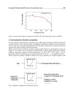
2. Conventional optical isolator
Optical isolators are one of the most important passive components in optical
communication systems. The function of an optical isolator is to let a light beam pass
through in one direction, that is, the forward direction only, like a one-way traffic. Optical
isolators are used to prevent destabilizing feedback of light that causes undesirable effects
such as frequency instability in laser sources and parasitic oscillation in optical amplifiers.
Ordinary optical isolators available commercially make use of the Faraday effect to produce
nonreciprocity. The Faraday effect is a magneto-optic phenomenon in which the
polarization plane of light passing through a transparent substance is rotated in the
presence of a magnetic field parallel to the direction of light propagation. The Faraday effect
occurs in many solids, liquids, and gases. The magnitude of the rotation depends on the
strength of the magnetic field and the nature of the transmitting substance. Unlike in the
optical activity (or natural activity), the direction of the rotation changes its sign for light
propagating in reverse. For example, if a ray traverses the same path twice in opposite
directions, the total rotation is double the rotation for a single passage. The Faraday effect is
thus non-reciprocal.
Fig. 1. Schematic structure of ordinary optical isolator.
Single Mode Operation of 1.5-μm Waveguide Optical Isolators
Based on the Nonreciprocal-loss Phenomenon
119
Figure 1 shows the schematic structure of an ordinary optical isolator. The isolator consists
of three components, i.e., a Faraday rotator, an input polarizer, and an output polarizer. The
Faraday rotator consists of a magnetic garnet crystal such as yttrium iron garnet and
terbium gallium garnet placed in a cylindrical permanent magnet and rotates the
polarization of passing light by 45°. As illustrated in Fig. 1, light traveling in the forward
direction (from A to B) will pass through the input polarizer and become polarized in the
vertical plane (indicated by Pi). On passing through the Faraday rotator, the plane of
polarization will be rotated 45° on axis. The output polarizer, which is aligned 45° relative to
the input polarizer, will then let the light pass through. In contrast, light traveling in the
reverse direction (from B to A) will pass through the output polarizer and become polarized
by 45° (indicated by Pr). The light will then pass through the Faraday rotator and experience
additional 45° of non-reciprocal rotation. The light is now polarized in the horizontal plane
and will be rejected by the input polarizer, which allows light polarized in the vertical plane
to pass through.
The ordinary optical isolator is bulky (therefore called a bulk isolator) and incompatible
with waveguide-based optical devices, so it cannot be used in PICs. It has, however,
superior optical characteristics (low forward loss and high backward loss) as shown in Fig. 2
[12]. Such good performance is a target in developing waveguide optical isolators.
Fig. 2. Optical characteristics of ordinary isolators available commercially [12]
3. Recent progress in waveguide optical isolators
3.1 How to make waveguide optical isolators
There are several strategies to develop waveguide optical isolators that can be integrated
monolithically with waveguide-based semiconductor optical devices on an InP substrate.
The strategies can be classified into two types. One is to use the Faraday effect as in
conventional bulk isolators. Transferring the principle of bulk isolators to a planer
waveguide geometry raises a number of inherent difficulties such as the discoherence of
polarization rotation induced by structural birefringence. Therefore new idea is needed to
use the Faraday effect in waveguide structure. Sophisticated examples are the Cotton-
Mouton isolator [13, 14] and the quasi-phase-matching (QPM) Faraday rotation isolator [15,
16]. The latter in particular have attracted attention in recent years because of its compact
techniques for producing the device. The other strategy to make waveguide isolators is to
use asymmetric magneto-optic effects that occur in semiconductor waveguides combined
with magnetic material. Leading examples are the nonreciprocal-phase-shift isolator [17-20]
and the nonreciprocal-loss isolator [21-26]. The nonreciprocal-loss isolator uses no rare-earth
garnet, so it is very compatible with standard semiconductor manufacturing processes. In
Advances in Optical and Photonic Devices
120
the following sections, we give the outline of the QPM Faraday rotation isolator and the
nonreciprocal-phase-shift isolator. The nonreciprocal-loss isolator, which has been
developed in our laboratory, is explained in detail in Section 4.
3.2 Quasi-phase-matching faraday rotation isolator
Figure 3 shows a schematic of the QPM Faraday rotation isolator. The device consists of a
Faraday rotator (non-reciprocal) section and a polarization rotator (reciprocal) section
integrated with a semiconductor laser diode that provides an TE-polarized output. The
Faraday rotator section consists of an AlGaAs/GaAs waveguide combined with a sputter-
coated film of magnetic rare-earth garnet CeY
2
Fe
5
O
x
. To obtain an appropriate polarization
rotation, this device uses the QPM Faraday effect in an upper-cladding that periodically
alternates between magneto-optic (MO) and non-MO media. Incident light of TE mode
traveling in the forward direction will first pass through the Faraday rotator section to be
rotated by +45°. The light then passes through the reciprocal polarization rotator section and
is rotated by -45°. Consequently, the light keeps its TE mode and passes through the output
edge. In contrast, backward traveling light of TE mode from the output filter is first rotated
by +45° in the reciprocal polarization rotator and then nonreciprocally rotated by +45° in the
Faraday rotator section. Consequently, backward light is transformed into a TM mode and
therefore has no influence on the stability of the laser because the TE-mode laser diode is
insensitive to TM-polarised light. The point of this device is TE-TM mode conversion in the
waveguide. At the present time, efficient mode conversion cannot be achieved, so practical
devices have yet to be developed.
Fig. 3. Schematic of QPM Faraday rotation isolator.
Using magneto-optical waveguides made of Cd
1-x
Mn
x
Te is effective to achieve efficient
mode conversion [27, 28]. Diluted magnetic semiconductor Cd
1-x
Mn
x
Te has the zincblende
crystal structure, the same as that of ordinary electro-optical semiconductors such as GaAs
and InP. Therefore, a single crystalline Cd
1-x
Mn
x
Te film can be grown epitaxially on GaAs
and InP substrates. In addition, Cd
1-x
Mn
x
Te exhibits a large Faraday effect near its
absorption edge because of the anomalously strong exchange interaction between the sp-
band electrons and localized d electrons of Mn2+. Almost complete TE-TM mode conversion
(98%+/-2% conversion) was observed in a Cd
1-x
Mn
x
Te waveguide layer on a GaAs substrate
[27, 28].
Single Mode Operation of 1.5-μm Waveguide Optical Isolators
Based on the Nonreciprocal-loss Phenomenon
121
3.3 Nonreciprocal phase-shift isolator
The nonreciprocal-phase-shift isolator uses a modified Mach-Zehnder interferometer that is
designed so that light waves traveling in two arms will be in-phase for forward propagation
and out-of-phase for backward propagation. Figure 4 shows the structure of the isolator
combined with a laser. The InGaAsP Mach-Zehnder interferometer consists of a pair of
three-guide tapered couplers, and an ordinary reciprocal 90° shifter on one of the arms.
Reciprocal phase shifting is achieved simply by setting a difference in dimensions or a
refractive index between the optical paths along two arms. A magnetic rare-earth garnet
YIG:Ce layer is placed on the arms to form a nonreciprocal 90° phase shifter on each arm.
The garnet layer was pasted on the interferometer by means of a direct-bonding technique.
Two external magnetic fields are applied to the magnetic layer on the two arms in an anti-
parallel direction, as shown in Fig. 4; this produces a nonreciprocal phase shift in the
interferometer in a push-pull manner. The isolator operates as follows. A forward-traveling
light wave from the laser enters the central waveguide of the input coupler and divided
between the two arms. During the light wave traveling in the arms, a -90° nonreciprocal
phase difference is produced, but it is canceled by a +90° reciprocal phase difference. The
divided two waves recouple at the output coupler, and output light will appear in the
central waveguide. In contrast, for a backward-traveling wave from the output coupler, the
nonreciprocal phase difference changes its sign to +90°, and it is added to the reciprocal
phase difference to produce a total difference of 180°. Consequently, output light will
appear in the two waveguides on both sides of the input coupler and not appear in the
central waveguide.
Fig. 4. Nonreciprocal-phase-shift isolator uses modified Mach-Zehnder interferometer.
4. Nonreciprocal loss phenomenon in magneto-optic waveguides
4.1 What is nonreciprocal loss phenomenon
One of the promising ways of creating waveguide optical isolators is by making use of the
phenomenon of nonreciprocal loss. This phenomenon is a nonreciprocal magneto-optic
phenomenon where——in an optical waveguide with a magnetized metal layer——the
propagation loss of light is larger in backward than in forward propagation. Using this
phenomenon can provide new waveguide isolators that use neither Faraday rotator nor
polarizer and, therefore, are suitable for monolithic integration with other optical devices on
Advances in Optical and Photonic Devices
122
an InP substrate. The theory of the nonreciprocal loss phenomenon was first proposed by
Takenaka, Zaets, and others in 1999 [29, 30]. After that, Ghent University-IMEC and Alcatel
reported leading experimental results in 2004; they made an isolator consisting of an
InGaAlAs/InP semiconductor waveguide combined with a ferromagnetic CoFe layer for
use at 1.3-μm wavelength [21, 22]. Inspired by this result, aiming to create polarization-
insensitive waveguide isolators for 1.5-μm-band optical communication systems, we have
been developing both TE-mode and TM-mode isolators based on this phenomenon. We
built prototype devices and obtained a nonreciprocity of 14.7 dB/mm for TE-mode devices
and 12.0 dB/mm for TM-mode devices——to our knowledge, the largest values ever
reported for 1.5-μm-band waveguide isolators. The TE-mode device consisted of an
InGaAsP/InP waveguide with a ferromagnetic Fe layer attached on a side of the waveguide
[24]. For the TM-mode device, instead of ordinary ferromagnetic metals, we used
ferromagnetic intermetallic compounds MnAs and MnSb, which are very compatible with
semiconductor manufacturing processes. The following sections provide the details on this
TM-mode isolator.
4.2 Structure of the TM-mode waveguide isolator
Figure 5 illustrates our TM-mode waveguide isolators with a cross section perpendicular to
the direction of light propagation. Two kinds of structure are shown. The device consists of
a magneto-optical planar waveguide that is composed of a TM-mode semiconductor optical-
amplifying waveguide (SOA waveguide) on an InP substrate and a ferromagnetic layer
attached on a top of the waveguide. To operate the SOA, a metal electrode is put on the
surface of the ferromagnetic layer (a driving current for the SOA flows from the electrode to
the substrate). Incident light passes through the SOA waveguide perpendicular to the figure
(z-direction). To operate the device, an external magnetic field is applied in the x-direction
so that the ferromagnetic layer is magnetized perpendicular to the propagation of light.
Light traveling along the waveguide interacts with the ferromagnetic layer.
Fig. 5. Typical TM-mode nonreciprocal-loss waveguide isolators.
The nonreciprocal propagation loss is caused by the magneto-optic transverse Kerr effect in
the magneto-optical planar waveguide. To put it plainly for TM-mode light, the
nonreciprocity is produced when light is reflected at the interface between the magnetized
Single Mode Operation of 1.5-μm Waveguide Optical Isolators
Based on the Nonreciprocal-loss Phenomenon
123
ferromagnetic layer and the SOA waveguide. The light reduces its intensity when reflected
from the ferromagnetic layer, which absorbs light strongly, and the reduction is larger for
backward propagating light than forward propagating light because of the transverse Kerr
effect. As a result, the propagation loss is larger for backward propagation (-z-direction)
than for forward propagation (z-direction). Figure 6 illustrates the operation of the isolator
on the propagation constant plane of the waveguide. The backward light is attenuated more
strongly than forward light. Since forward light is also attenuated, the SOA is used to
compensate for the forward loss; the SOA is operated so that the net loss for forward
propagation will be zero. Under these conditions, the waveguide can act as an optical
isolator.
Fig. 6. Principle of nonreciprocal-loss waveguide isolator.
4.3 Theory of nonreciprocal loss in the waveguide isolator
Let us calculate the nonreciprocal loss in the magneto-optic waveguide and design
optimized structure for the isolator device, using electromagnetic simulation. In the TM-
mode isolator, light traveling along the SOA waveguide extends through the cladding layer
into the ferromagnetic layer to a certain penetration depth and interacts with magnetization
vector in the ferromagnetic layer (see Fig. 5). Therefore, the thicknesses of the cladding layer
and the ferromagnetic layer greatly affect the performance—the isolation ratio and forward
loss (insertion loss) —of the isolator as follows:
i. A large isolation ratio can be obtained at small cladding-layer thickness because a thin
cladding layer easily lets light through into the ferromagnetic layer to produce a large
magneto-optic interaction. Therefore, the cladding layer has to be thin as long as the
amplifying gain of the SOA can compensate for the absorption loss of light in the
ferromagnetic layer.
ii. The ferromagnetic layer has to be thicker than its penetration depth of light. If it is not,
light leaks out of the upper part of the ferromagnetic layer and is needlessly absorbed
by the metal electrode. This reduces the isolation ratio because part of the propagating
light in the device cannot interact with the ferromagnetic layer.
To determine the optimum thicknesses of the cladding and ferromagnetic layers, we
calculated the isolation ratio and the insertion loss of the device as a function of the
Advances in Optical and Photonic Devices
124
thicknesses by means of two-dimensional electromagnetic simulation based on the finite
difference method (FDM).
In this device, the structure of the SOA has an influence on the device performance as well.
However, the SOA structure cannot be changed greatly under the condition that the SOA
should amplify TM-mode light at 1.5-μm-band wavelength. Therefore, we focus only on the
thicknesses of the cladding and ferromagnetic layers to optimize the device performance.
The nonreciprocity of the device is caused by the off-diagonal elements in the dielectric
tensor of the ferromagnetic layer. The dielectric tensor of each layer in the device is given by
00
0
0
n
nn
n
j
j
ε
ε
εα
α
ε
⎛⎞
⎜⎟
=
⎜⎟
⎜⎟
−
⎝⎠
, (3-1)
where ε
n
is the diagonal element of the tensor in nth layer. The off-diagonal element α is 0
except in the ferromagnetic layer. Using these tensors, we write the Maxwell’s equations in
an isotropic charge-free medium as
0
0
()0
n
n
j
j
ω
εε
ωμ
ε
∇× =
∇× =−
∇⋅ =
HE
EH
E
. (3-2)
Taking the rot of the second equation and using the first equation, we obtain the equation,
22
0
()
n
k
ε
∇∇⋅ −∇ =EE E
, (3-3)
where we used
2
()()
∇
×∇× =∇∇⋅ −∇EEE, and
000
2k
ω
με π λ
== is the free-space
propagation constant. Using the second and third equations in (3-2) and
z
j
β
∂
= , the z
component of eq. (3-3) can be written as
22 22 2
0
00
()
xz
y
znz
y
zx
n
EEk EjkE H
αωμ
εβ α
ε
∂+∂+ − = − ∂, (3-4)
where β is the propagation constant in the device along z direction, E
t
and H
t
(t = x, y, z) are
electric field (parallel to t axis) and magnetic field (parallel to t axis) of the light.
The y and z components of the first equation in (3-2) can be given by the equations for TM-
mode light (E
x
= H
y
= H
z
= 0),
00
00
zx z n
y
y
x
y
nz
HEjE
HEjE
α
ωε ωε ε
α
ωε ωε ε
∂
=− +
−∂ = +
. (3-5)
Substituting the first equation of (3-5) into eq. (3-4) gives the equation for E
z
,
22
22 22
0
0
0
xz yz n z
n
k
EEk E
α
εβ
ε
⎛⎞
∂
+∂ + − − =
⎜⎟
⎝⎠
. (3-6)
Using eqs. (3-5), we can express E
z
with H
x
as
Single Mode Operation of 1.5-μm Waveguide Optical Isolators
Based on the Nonreciprocal-loss Phenomenon
125
22
0
()
n
z
y
xx
nn
j
EHH
ε
αβ
ωε ε α ε
⎛⎞
=∂−
⎜⎟
−
⎝⎠
. (3-7)
From eqs. (3-6) and (3-7), we can obtain the scalar wave equation for magnetic field H
x
of
TM waves in each layer. The wave equation in non-magnetic layers (α=0) is given by
22 22
0
0 ( )
xx yx x n
HHH k
φ
φεβ
∂+∂+= = −. (3-8)
For the ferromagnetic layer, the wave equation has first-order and third-order derivative
terms because of the nonzero off-diagonal element α in the dielectric tensor. For ordinary
values of α in ferromagnetic materials, third-order terms of
2
x
y
x
H∂∂ and
3
y
x
H∂ are small
and can be ignored. In consequence, the wave equation in the ferromagnetic layer is given by
22
22 22
0
0
0 ( )
n
xx yx yx x n
n
k
HH HH k
ε
α
ϕϕ ϕεβ
αβ ε
∂+∂− ⋅∂+= = −− . (3-9)
Because of the nonzero off-diagonal elements in the dielectric tensor, the equation involves a
linear term in the propagation constant β; this leads to a nonreciprocal solution to the
propagation direction. The nonreciprocal solution gives a difference in absorption
coefficient between forward (z-direction) and backward (-z-direction) TM waves and,
therefore, gives the isolation ratio (or the difference between forward absorption and
backward absorption) in the device.
To solve the wave equation numerically, we partition the domain in space using a mesh x
0
,
x
1
,…x
p
,… in x direction and mesh y
0
, y
1
,…y
q
,… in y direction with a mesh width (the
difference between two adjacent space points) of m in x direction and n in y direction. We
represent the magnetic field on each mesh point (x
p
, y
q
) by H
p,q
. Using a second-order central
difference for the space derivative at position (x
p
, y
q
), we obtain the recurrence equation
1, 1, , 1 , 1 ,
2222 22
1111 22
()0
p q p q pq pq pq
HHHH H
mmnn mn
φ
−+ −+
+
+++−−=
(3-10)
for eq. (3-8), and recurrence equation
1, 1, , 1 , 1 , 1 , 1 ,
222 2 22
111 1 22
()0
22
nn
p q p q pq pq pq pq pq
HHHHHH H
mmn n n n mn
εε
ϕϕϕ
αβ αβ
−+ − −+ +
++++−+−−= (3-11)
for eq. (3-9). Solving eqs. (3-10) and (3-11) numerically, we can calculate the forward and
backward propagation loss and the isolation ratio, as a function of the thicknesses of the
cladding layer and the ferromagnetic layer, where the SOA is not operated. (In actual
operation, the SOA is operated so that it compensates for the forward propagation loss.)
Before calculating the optimum thicknesses of the cladding and ferromagnetic layers, we
must design the appropriate structure of the SOA region to amplify 1.5-μm TM-mode light.
The structural parameters we used for the SOA was as follows. The substrate is a highly
doped n-type InP (refractive index n = 3.16). The constituent layers of the SOA are: (i) lower
guiding layer: 100-nm thick InGaAlAs (bandgap wavelength λ
g
= 1.1 μm, n = 3.4), (ii) MQW:
five InGaAs quantum wells (-0.4% tensile-strained, 15-nm-thick well, n
MQW
= 3.53) with six
InGaAlAs barriers (+0.6% compressively strained, 12-nm-thick barrier, λ
g
= 1.2 μm), and (iii)
upper guiding layer: 100-nm-thick InGaAlAs (λ
g
= 1.1 μm, n = 3.4).
Advances in Optical and Photonic Devices
126
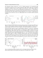
Fig. 7. (a) Forward absorption loss (propagation loss) and (b) isolation ratio (nonreciprocity)
in the device as a function of Ferromagnetic-layer thickness and cladding layer thickness,
calculated for 1.55-μm TM mode.
For the isolator with this SOA region, we calculated the propagation loss and the isolation
ratio, using the method described above. Figure 7 shows an example of the results, i.e., (a)
the absorption loss for forward propagation and (b) the isolation ratio as a function of the
InP-cladding and ferromagnetic layer thicknesses. In this simulation, we assumed a device
consisting of a ridge-shaped optical amplifying waveguide (see Fig. 5(b)) covered with a
ferromagnetic MnAs layer and an Au-Ti metal electrode. The reason we used manganese
pnictides as the ferromagnetic layer will be explained in Section 5. The parameters we used
in the simulation are given in Table 1. The forward absorption loss in the device is large and
the isolation ratio is small at small MnAs thickness because part of the propagating light in
the device leaks out of the MnAs layer and is needlessly absorbed by the Au-Ti electrode. As
MnAs layer thickness increases, forward absorption loss decreases and isolation ratio
increases, both approaching a constant in MnAs layers thicker than 200 nm. This means that
light penetrates to a depth of about 200 nm in the MnAs layer. Therefore, more than 200 nm
can be considered a necessary and sufficient thickness for the MnAs layer when fabricating
devices.
Figure 7 also shows that both the isolation ratio and the absorption loss increase as the
thickness of the InP-cladding layer decreases. This is so because a thinner cladding layer lets
a higher percentage of light through into the MnAs layer, producing a larger interaction. A
thin cladding layer is preferable for obtaining a large isolation ratio as long as the forward
absorption loss can be compensated for by the amplifying gain of the SOA. We expected an
SOA gain of 16 dB/mm, and therefore decided that the optimum thickness of the cladding
layer was 350 nm.
Figure 8 illustrates the distribution profile of light traveling in the isolator for forward and
backward propagation, with the results calculated for a device with a 350-nm InP-cladding
layer and a 200-nm MnAs layer. Figures 8(a-1) and 8(b-1) show the contour lines for TM
magnetic field vector intensity—large magnetic fields in the central part—on the cross
Single Mode Operation of 1.5-μm Waveguide Optical Isolators
Based on the Nonreciprocal-loss Phenomenon
127
Table 1. Example of parameters used for calculating device characteristics.
Fig. 8. Distribution profile of light traveling in isolator, calculated for 1.55 μm TM mode,
with a 350-nm cladding layer and a 200-nm MnAs layer: cross section of distribution for (a-
1) forward and (b-1) backward propagating light; distribution along vertical center line
(dashed lines in (a-1) and (b-1)) of device for (a-2) forward and (b-2) backward propagating
light.
Advances in Optical and Photonic Devices
128
section (x-y plane) of the device, where Fig. 8(a-1) is for forward propagating light and Fig.
8(b-1) is for backward light. Figures 8(a-2) and 8(b-2) depict the magnetic field vector
intensity along the vertical center line (dashed lines in Figs. 8(a-1) and 8(b-1)) of the device,
where Fig. 8(a-2) is for forward light and Fig. 8(a-2) is for backward light. Unlike forward
propagating light, backward propagating light shifts its distribution tail to the MnAs layer
and, therefore, suffers a larger absorption loss in the MnAs layer. Therefore, the propagation
loss of light is larger in backward than in forward propagation.
5. Prototype device with ferromagnetic MnAs
5.1 Using manganese pnictides as a ferromagnetic material
The point of our device is its use of manganese arsenide (MnAs) as a ferromagnetic material,
instead of ordinary ferromagnetic metals such as Fe and Co. In our device structure——
which is necessary for TM-mode operation——the ferromagnetic layer used to produce the
nonreciprocity is also used as a contact to supply a driving current to the SOA. This means
that the ferromagnetic layer has to meet a dual requirement of (i) producing a large Kerr
effect at the wavelength of 1.5 μm and of (ii) providing a low-barrier contact for p-type III-V
semiconductors. Ordinary ferromagnetic metals are not suited for this purpose because they
produce a Schottky barrier on III-V semiconductors, thereby producing a high-resistance
contact on the contact layer. In addition, during contact annealing, they produce
undesirable nonferromagnetic compounds such as FeAs and CoAs at the contact interface
and simultaneously degrade the microscopic flatness of the interface; this reduces optical
nonreciprocity in the device. To solve these problems, we used manganese arsenide, MnAs,
for the ferromagnetic layer. MnAs are ferromagnetic, intermetallic compounds with a NiAs-
type hexagonal structure (see Fig. 9). They can be grown epitaxially on GaAs, InP, and
related semiconductors by means of molecular beam epitaxy (MBE), without producing a
solid-phase reaction at the interface [31-34]. MnAs is suitable ferromagnetic materials for
our device because they have enough Kerr effect at 1.5-μm wavelength to produce practical
nonreciprocity and, at the same time, can make a low-resistance contact on III-V
semiconductors. The Currie temperature is 40°C for MnAs.
Fig. 9. Structure of manganese pnictides.
Single Mode Operation of 1.5-μm Waveguide Optical Isolators
Based on the Nonreciprocal-loss Phenomenon
129
To take the first step, we made a device with a MnAs layer because the epitaxial growth
technology of MnAs layers on III-V semiconductors was well established [31-33]. To reduce
the propagation loss of light and obtain a single-mode operation, we used the ridge
waveguide structure with a large lateral-confinement factor (see Fig. 5(b)). In the following
sections, we provide details of the fabrication process and operation characteristics of the
device that uses ferromagnetic MnAs.
5.2 Constructing the device
Figure 10(a) is a cross-sectional diagram of our TM-mode waveguide isolator with a
ferromagnetic MnAs layer. The MnAs layer covers the SOA surface, and two interface layers
(a highly doped p-type InGaAs contact layer and a p-type InP cladding layer) are inserted
between the two. The InGaAs contact layer has to be thin so that 1.5-μm light traveling in
the SOA will extend into the MnAs layer (the absorption edge of the contact layer is about
1550 nm). An Au/Ti double metal layer covers the MnAs layer, forming an electrode for
current injection into the SOA. Light passes through the SOA waveguide in a direction
perpendicular to the figure (z direction). An Al
2
O
3
insulating layer separates the SOA
surface from the Au-Ti electrode except on the contact region. Incident light passes through
the SOA waveguide perpendicular to the figure (z direction).
Fig. 10. (a) Schematic cross section of our waveguide isolator for 1.5-μm TM mode,
consisting of a ridge-shaped optical amplifying waveguide covered with a MnAs layer
magnetized in x-direction. Light propagates along z-direction. (b) SEM cross section of
device.
On the basis of the simulation results mentioned in Section 4.3, we fabricated a device as
follows. The substrate was a highly doped, [100]-oriented n-type wafer of InP. The SOA was
formed on the substrate by metalorganic vapor-phase epitaxy (MOVPE). The MQW showed
a photoluminescence peak at 1.54 μm——this means that the SOA had a gain peak at 1.54
μm. The thicknesses of the p-InP cladding and p
+
InGaAs contact layers were set to be 350
nm and 10nm. After the formation of the SOA, a 200 nm MnAs layer was grown on the
surface of the p
+
InGaAs contact layer by MBE. The wafer was first heat treated at about 550
Advances in Optical and Photonic Devices
130
o
C under As
2
flux in the MBE chamber to remove a native oxide layer on the contact layer.
The wafer temperature was then lowered to 200
o
C, and the As
2
flux was kept supplying to
form an As template on the surface. This As template on the surface is important to grow
high quality MnAs, as in the growth of MnAs layers on GaAs
[31, 32] and InP [33]. The
surface of the InGaAs contact layer with the As template showed spotty refraction high
energy electron diffraction (RHEED) pattern. After that, Mn and As
2
fluxes were supplied
on the surface to grow a 200 nm MnAs thin film. During the growth process, we confirmed
(1×2) reconstruction in RHEED, indicating that the MnAs structural properties were
improved. An X-ray diffraction pattern showed strong MnAs peaks in [1-100] directions.
After the growth of MnAs, the ridge waveguide structure was formed as follows. First, a
photoresist mask in the form of a 2-μm-wide waveguide pattern was made on the surface of
the MnAs layer. Then, the MnAs layer, InP cladding layer, and InGaAs contact layers were
selectively etched in this order to fabricate a ridge waveguide—the MnAs layer was etched
by reactive ion etching with Ar, and the cladding and the contact layers were wet-etched
with a Br
2
-HBr-H2O solution. An Al
2
O
3
layer was deposited on this ridge waveguide using
electron-beam (EB) evaporation. Then, the Al
2
O
3
on the contact layer was removed using a
lift-off process. Finally, a Ti layer and an Au layer were deposited to make a top electrode,
using EB evaporation. This was the process we used to fabricate the structure depicted in
Fig. 10(a). Finally, both ends of the device were cleaved, and the cleaved surfaces were left
uncoated. Figure 10(b) is a cross section of the device as observed with scanning electron
microscopy (SEM).
Fig. 11. Magnetization curve for MnAs layer, measured with a AGFM. MnAs layer can be
easily magnetized along [011] direction of InP substrate. In contrast, magnetization is
difficult along [01-1] direction.
Single Mode Operation of 1.5-μm Waveguide Optical Isolators
Based on the Nonreciprocal-loss Phenomenon
131
MnAs thin films grown on the InGaAs contact layer showed strong magnetocrystalline
anisotropy——an intrinsic property of a ferrimagnet, independent of grain size and shape;
the MnAs thin films were easily magnetized along the [011] direction of the InP substrates.
Based on the fact, we formed the waveguide stripe parallel to the [0-11] direction of the InP
substrate, and applied an external magnetic field to the [011] direction (x-direction in Fig.
10). However, in addition to the magnetocrystalline anisotropy, the shape anisotropy of the
MnAs layer must be taken into consideration for the fabricated device because our device
(or the MnAs layer) had the form of the 2-μm-wide waveguide structure. Therefore, we
confirmed a magnetization curve of the MnAs layer in our device before measuring device
characteristics. Figure 11 shows a plot of the magnetization curve, measured by alternating
gradient force magnetometry (AGFM). Along the [011] direction of the InP substrate, the
MnAs layer showed a soft hysteresis curve and was easily magnetized with a small coercive
field of 0.07 T. In contrast, the magnetization was not easy along the [01-1] direction and was
insufficient even in a magnetic field of 0.5 T. This means that the magnetocrystalline
anisotropy is larger than the shape anisotropy in our device, and the device was expected to
work with an external magnetic field of 0.07-0.1 T (initial magnetizing requires 0.15-0.2 T).
5.3 Device operation
We confirmed that the device functioned successfully as an optical isolator with
nonreciprocal loss for TM-polarized, 1.5-μm light. Figure 12 shows our experimental setup
for the measurement. It consisted of a wavelength-tunable laser, two polarization
controllers, two circulators, two optical switches, an output coupler, an optical power meter,
and an optical spectrum analyzer (OSA). Light from a tunable laser was transmitted to the
device through a polarization controller and a circulator. The light was transferred into and
out of the device using lensed-fiber couplers. A magnetic field was applied using a
permanent magnet along the [011] direction of the device, i.e., parallel to the surface of the
device and perpendicular to the direction of light propagation. Light propagation in the
device was switched between forward direction (switch node 1–upper circulator–device–
lower isolator– switch node 4 in Fig. 12) and backward direction (node 2–lower circulator–
Fig. 12. Experimental setup for measuring isolation ratio and propagation loss of light in
device.
Advances in Optical and Photonic Devices
132
device–upper isolator–node 3) by controlling the optical switches. The intensity of light
transmitted in the device (or the output light from the device) was measured using the
optical spectrum analyzer and the power meter. The output of the tunable laser was set to 5
dBm, and the magnetic field for the device was set to 0.1 T. During measurement, the device
was kept at 20
o
C and operated with a SOA driving current of 100 mA. The MnAs layer
successfully provided a low-resistance contact for the InGaAs contact layer. The voltage
drop across the device 0.65 mm in length was only 1.7 V (SOA diode drop 0.9 V plus ohmic
contact drop 0.8 V), whereas the drop across a control device with Fe-Ni layers instead of
MnAs was 3.0 V (SOA diode drop 0.9 V plus ohmic contact drop 2.1 V) [35].
Figure 13 shows the transmission spectra of the device with a length of 0.65 mm. The
intensity of the output light from the device is plotted as a function of wavelength for
forward (dashed line) and backward (solid line) propagation of (a) TM-polarized and (b)
TE-polarized light. The wavelength of incident light was fixed at 1.54 μm, which was the
gain peak wavelength of the SOA. For TM-mode light, the output intensity changed by 4.7
dB by switching the direction of light propagation. The device operated efficiently as a TM-
mode isolator with an isolation ratio of 7.2 dB/mm (= 4.7 dB/0.65 mm). In contrast, the
output intensity for TE-mode light was not dependent on the direction of the light
propagation. Small periodic ripples in amplified spontaneous emission spectra are shown in
Fig. 13. They are caused by Fabry-Perot interference due to reflection from cleaved facets;
the period was consistent with the value predicted from the length and effective refractive
index of the device. The inset in Fig 13(a) is the near-field pattern of the TM-mode forward
propagating light and shows that the device operated successfully in a single mode.
Fig. 13. Transmission spectra of device for forward transmission (dashed line) and backward
transmission (solid line), measured for (a) TM-mode and (b) TE-mode, at 1.54-μm
wavelength, 100-mA driving current, and 0.1-T magnetic field. Device is 0.65 mm long. Data
on transmission intensity include loss caused by measurement system. Inset is near-field
pattern of TM-mode forward propagating light.
Single Mode Operation of 1.5-μm Waveguide Optical Isolators
Based on the Nonreciprocal-loss Phenomenon
133
The data of transmission intensity in Fig. 13 include the loss caused by the measurement
system. To examine the intrinsic transmission loss of the device, we measured the
transmission intensity for devices with different lengths. Figure 14 shows the results, i.e., the
output intensity for forward and backward transmission as a function of device length
(isolation ratio is also plotted). The slope of the forward line gives the intrinsic transmission
loss (or absorption loss) per unit length. We estimated that forward loss in the device was
10.6 dB/mm—still large for practical use. This is so because the gain of the SOA was lower
than we had expected, and therefore, insufficient to compensate for the intrinsic
transmission loss in the device. The loss caused by the measurement system can also be
calculated using the vertical-axis intercept of the forward line and the output intensity of the
tunable laser. It was estimated to be 28 dB—output coupler loss 3 dB plus lensed-fiber
coupling loss 12.5 dB/facet × 2 between the measurement system and the device.
Fig. 14. Transmission intensity as a function of device length, measured for 1.54 μm TM
mode, with 100-mA driving current and 0.1-T magnetic field. Isolation ratio is also plotted.
Figure 15 is a plot of the isolation ratio, as a function of wavelength from 1.53 to 1.55 μm.
The device was 0.65-mm long. The output intensities for forward and backward
propagations are also plotted (including the measurement system loss). In this range of
wavelength, the isolation ratio was almost constant. The isolation ratio 7.2 dB/mm of this
waveguide isolator was still small for practical use. In addition, the device was unable to
operate at temperatures higher than room temperature because the Currie temperature of
MnAs is only 40°C. To improve the device performance, we have to seek other superior
ferromagnetic materials. In the next section, we present a device that uses MnSb instead of
MnAs.
Advances in Optical and Photonic Devices
134
Fig. 15. Isolation ratio as a function of a wavelength from 1.53 to 1.55 μm for a 0.65-mm long
device. Transmission intensity is also plotted for forward and backward propagation
(including measurement system loss).
6. Conclusion
An important element for developing photonic integrated circuits is waveguide optical
isolators that can be monolithically combined with other waveguide-based devices such as
lasers. One promising way of creating such waveguide isolators is by using the
phenomenon of nonreciprocal loss in magneto-optical waveguides. Making use of this
phenomenon, we have been developing TE- and TM-mode waveguide isolators operating at
1.5-μm telecommunication band. As a fromagnetic material for the magneto-optical
waveguide isolator, manganese pnictides such as MnAs are more superior than ordinary
ferromagnetic metals because they can be formed on GaAs, InP, and related materials using
semiconductors manufacturing process. Although MnAs is not common material at present
for integrated optics, it will soon bring technical innovation in functional magneto-optic
devices for large-scale photonic integrated circuits.
7. References
[1] O. Wada; T. Sakurai; T. Nakagami IEEE J. Quantum Electron. 1986, 22, 805-821.
[2] T. L. Koch; U. Koren IEEE J. Quantum Electron. 1991, 27, 641-653.
[3] A. A. M. Staring; L. H. Spiekman; J. J. M. Binsma; E. J. Jansen; T. van Dongen; P. J. A.
Thijs; M. K. Smit; B. H. Verbeek IEEE Photon. Technol. Lett. 1996, 8, 1139-1141.
[4] Nagarajan, R.; Joyner, C.H.; Schneider, R.P., Jr.; Bostak, J.S.; Butrie, T.; Dentai, A.G.;
Dominic, V.G.; Evans, P.W.; Kato, M.; Kauffman, M.; Lambert, D.J.H.; Mathis, S.K.;
Mathur, A.; Miles, R.H.; Mitchell, M.L.; Missey, M.J.; Murthy, S.; Nilsson, A.C.;
Single Mode Operation of 1.5-μm Waveguide Optical Isolators
Based on the Nonreciprocal-loss Phenomenon
135
Peters, F.H.; Pennypacker, S.C.; Pleumeekers, J.L.; Salvatore, R.A.; Schlenker, R.K.;
Taylor, R.B.; Huan-Shang Tsai; Van Leeuwen, M.F.; Webjorn, J.; Ziari, M.; Perkins,
D.; Singh, J.; Grubb, S.G.; Reffle, M.S.; Mehuys, D.G.; Kish, F.A.; Welch, D.F. IEEE J.
Select. Topics Quantum Electron. 2005, 11, 50-65.
[5] N. Sugimoto; H. Terui; A. Tate; Y. Katoh; Y. Yamada; A. Sugita; A. Shibukawa; Y. Inoue
J. Lightwave Technol. 1996, 14, 2537-2546.
[6] M. Levy; R. M. Osgood; H. Hegde; F. J. Cadieu; R. Wolfe; V. J. Fratello IEEE Photonics
Technol. Lett. 1996, 8, 903-905.
[7] M. Fehndrich; A. Josef; L. Wilkens; J. Kleine-Börger; N. Bahlmann; M. Lohmeyer; P.
Hertel; H. Dötsch Appl. Phys. Lett.1999, 74, 2918-2920.
[8] J. Fujita; M. Levy; R. M. Osgood; L. Wilkens; H. Dotsch Appl. Phys. Lett. 2000, 76, 2158-
2160.
[9] M. Levy IEEE J. Sel. Top. Quantum Electron. 2002, 8, 1300-1306.
[10] J. S. Yang; J. W. Roh; S. H. Ok; D. H. Woo; Y. T. Byun; W. Y. Lee; T. Mizumoto; S. Lee
IEEE Trans. Magn. 2005, 41, 3520-3522.
[11] T. R. Zaman; X. Guo; R. J. Ram IEEE Photonics Technol. Lett. 2006, 18, 1359-1361.
[12]
[13] K. Ando; N. Takeda; N. Koshizuka; T. Okuda J. Appl. Phys. 1985, 57, 1277-1281.
[14] H. Dammann; E. Pross; G. Rabe; W. Tolksdorf; M. Zinke Appl. Phys. Lett. 1986, 49,
1755-1757.
[15] B. M. Holmes; D. C. Hutchings Appl. Phys. Lett. 2006, 88, 061116.
[16] B. M. Holmes; D. C. Hutchings Proc. of IEEE Lasers and Electro-Optics Society 2006,
897-898.
[17] H. Yokoi; T. Mizumoto; N. Shinjo; N. Futakuchi; Y. Nakano Appl. Optics 2000, 39, 6158-
6164.
[18] H. Yokoi; T. Mizumoto; Y. Shoji Appl. Optics 2003, 42, 6605-6612.
[19] K. Sakurai; H. Yokoi; T. Mizumoto; D. Miyashita; Y. Nakano Jpn. J. Appl. Phys. 2004, 43,
1388-1392.
[20] Y. Shoji; T. Mizumoto Appl. Optics 2006, 45, 7144-7150.
[21] M. Vanwolleghem; W. Van Parys; D. Van Thourhout; R. Baets; F. Lelarge; O. Gauthier-
Lafaye; B. Thedrez; R. Wirix-Speetjens; and L. Lagae Appl. Phys. Lett. 2004, 85,
3980-3982.
[22] W. Van. Parys; B. Moeyersoon; D. Van. Thourhout; R. Baets; M. Vanwolleghem; B.
Dagens; J. Decobert; O. L. Gouezigou; D. Make; R. Vanheertum; L. Lagae Appl.
Phys. Lett. 2006, 88, 071115.
[23] H. Shimizu; Y. Nakano Jpn. J. Appl. Phys. 2004, 43, L1561-L1563.
[24] H. Shimizu; Y. Nakano IEEE J. Lightwave Technol. 2006, 24, 38-43.
[25] T. Amemiya; H. Shimizu; Y. Nakano; P. N. Hai; M. Yokoyama; M. Tanaka Appl. Phys.
Lett. 2006, 89, 021104.
[26] T. Amemiya; H. Shimizu; P. N. Hai; M. Yokoyama; M. Tanaka; Y. Nakano Appl. Optics
2007, 46, 5784-5791.
[27] W. Zaets; K. Ando Appl. Phys. Lett. 2000, 77, 1593-1595.
[28] V. Zayets; M. C. Debnath; K. Ando Appl. Phys. Lett. 2004, 84, 565-567.
Advances in Optical and Photonic Devices
136
[29] M. Takenaka; Y. Nakano Proc. of IEEE Conference on Indium Phosphide and Related
Materials 1999, 289-292.
[30] W. Zaets; K. Ando IEEE Photonics Technol. Lett. 1999, 11, 1012-1014.
[31] M. Tanaka; J. P. Harbison; G. M. Rothberg Appl. Phys. Lett. 1994, 65, 1964-1966.
[32] L. Daweritz; L. Wan; B. Jenichen; C. Herrmann; J. Mohanty; A. Trampert; K. H. Ploog J.
Appl. Phys. 2004, 96, 5052-5056.
[33] M. Yokoyama; S. Ohya; M. Tanaka Appl. Phys. Lett. 2006, 88, 012504.
[34] H. Akinaga; K. Tanaka; K. Ando; T. Katayama J. Cryst. Growth 1995, 150, 1144-1149.
[35] T. Amemiya; H. Shimizu; Y. Nakano, Proc. of IEEE Conference on Indium Phosphide
and Related Materials 2005, 303-306.
[36] Y. Ogawaa; T. Amemiya; H. Shimizu; Y. Nakano; H. Munekata Proc. of International
Symposium on Compound Semiconductors 2007, TuC-P22.
8
GaAs/AlOx Nonlinear Waveguides
for Infrared Tunable Generation
E. Guillotel, M. Ravaro, F. Ghiglieno, M. Savanier, I. Favero,
S. Ducci, and G. Leo
Laboratoire Matériaux et Phénomènes Quantiques, UMR 7162, Université Paris Diderot
France
1. Introduction
New optical sources in the near- and mid-infrared (NIR/MIR respectively) have recently
attracted a growing attention for potential applications in telecommunication systems (Yoo,
1996), spectroscopy (Chen et al., 1999; Arie et al., 2002), gas sensing (Lancaster et al., 1999),
and quantum information (Gisin et al., 2002; Sergienko & Jaeger, 2003). In this respect,
guided-wave frequency conversion is an appealing solution, due to its efficiency,
compactness and tunability of the output wavelength. In this process, three guided modes
coupled by the material optical nonlinearity exchange power during propagation; provided
that their phase-velocity mismatch is absent or cancelled, such interaction allows the
efficient transfer of power from the injected pump modes to a new-frequency generated
mode, according to energy conservation (Boyd, 2008).
After the demonstration of a few original phase-matching schemes, nonlinear waveguides
based on gallium arsenide (GaAs) have carved out a prominent position in the panorama of
integrated frequency converters. Among their main assets, in comparison with alternative
material systems: a higher nonlinear coefficient, a wider infrared transparency range, and
potential monolithic integration with a laser diode pump source. On the other hand,
conversion efficiency in such devices is still affected by non-negligible scattering loss, in
spite of recent technological developments. Due to this limitation, no optical parametric
oscillator has been reported to date in GaAs waveguides, whereas it was demonstrated long
ago in lithium niobate (LiNbO
3
) waveguides (Bortz et al., 1995).
In this chapter we focus on GaAs/AlAs nonlinear waveguides, where phase-matched three-
wave mixing can be performed thanks to form birefringence. This is obtained by oxidizing a
few AlAs thin layers in the waveguide core, with AlAs being transformed into a low-index
non-stoichiometric aluminium oxide (hereafter referred to as AlOx). Although all different χ
(2)
processes have been reported so far, these devices especially lend themselves to parametric
down-conversion towards mid-infrared, and are promising candidates as compact sources for
infrared spectroscopy. In the first section we briefly summarize the state-of-the art of mid-
infrared tunable coherent sources, focusing on frequency converters. At present, none of these
sources fully meets the main requirements of practical spectroscopic systems. In section two,
we describe the phase-matching principle and the design guidelines of GaAs/AlOx
waveguides, while the fabrication process and its crucial issues are detailed in section three.
Advances in Optical and Photonic Devices
138
The recent progress in terms of infrared generation efficiency and tunability will be the object
of the fourth section. Finally, the fifth section is devoted to work in progress towards the
realization of a semiconductor optical parametric oscillator.
2. Scientific context: sources for infrared spectroscopy
2.1 Laser diodes and bulk frequency converters
Mid-infrared spectrum is of strong scientific and technological interest for spectroscopy, as
several molecules exhibit their fundamental rotational-vibrational resonances in this region,
with absorption spectra highly specific to their atomic structure. As mid-infrared absorption
lines are very strong, molecule concentrations as low as parts per-billion can be detected by
means of laser-based detectors. In the near-infrared, where only overtone resonances can be
excited, absorption peaks are weaker, and the corresponding detection thresholds several
orders of magnitude higher. Nevertheless, many measurements are still performed at
wavelengths below 2 µm, due to the relative lack of suitable laser sources at longer
wavelengths. Infrared spectroscopy requires continuously tunable sources, with
compactness and room temperature operation highly desirable. In the mid-infrared, the
present state of the art for this type of devices includes diode lasers and sources based on
nonlinear frequency conversion (Sorokina & Vodopyanov, 2003).
The main representatives of the former category are antimonide diodes and quantum-
cascade lasers. Both are proven to produce significant continuous wave (CW) output power
at room temperature in the 2-3 and in the 4-9 µm range, respectively, while maintaining
single mode operation and being reproducibly tunable in a manner suitable for
spectroscopy. Tuning is typically accomplished by changing either the temperature or the
injected current, on an overall range limited to few tens of nanometres.
A versatile alternative to laser diodes is represented by sources based on χ
(2)
nonlinear
processes. For MIR generation, frequency conversion involves the use of an intense “pump”
wave (generated by a laser of angular frequency ω
p
), which is coupled to an input wave at
ω
s
(the “signal”), with an “idler” generated at the difference frequency ω
p
-ω
s
. The input
signal photons can be provided by either a second injected laser beam or quantum noise. In
the former case, the interaction is generally performed in a single-pass configuration and is
referred to as difference-frequency generation (DFG). The latter process is called parametric
fluorescence. Since the single-pass gain is low, it is generally exploited by resonantly
enhancing the signal or the idler wave in a cavity containing the nonlinear medium, i.e. an
optical parametric oscillator (OPO).
DFG and OPOs are largely employed for the generation of mid-infrared, as they can
produce coherent radiation in any temporal format and over a wide spectral range, only
limited by the transparency of the nonlinear crystal. For both these processes, one of the
main issues is the fulfilment of the phase-matching condition. For the signal and idler waves
to be continuously fed by the pump as the beams propagate through the crystal, the three
waves must stay unvaried in their initial phase relation, in contrast with crystal dispersion.
The classical approach to achieve phase-matched propagation consists in compensating
dispersion in a birefringent nonlinear crystal. More convenient quasi-phase matching (QPM)
relies on a microstructured crystals where the second-order susceptibility is periodically
inverted, so as to keep the three waves into the correct phase relation. This technique, for
long time the prerogative of ferroelectric crystals, further reinforced LiNbO
3
position as the
nonlinear crystal of choice, including for the fabrication of infrared sources. The