Micro Electronic and Mechanical Systems 2009 Part 6 pptx
Bạn đang xem bản rút gọn của tài liệu. Xem và tải ngay bản đầy đủ của tài liệu tại đây (1020.01 KB, 35 trang )
Micro Electronic and Mechanical Systems
166
mechanical properties of thin films and various values have been measured (Ammaleh,
2003; Dual, 2004; Yi, 1999). Reported variations in measured values were large requiring
extensive research in order to evaluate repeatability, accuracy and data reliability of various
measurement methods for mechanical properties of MEMS materials. Therefore,
development of international standards on MEMS materials and their properties
measurement methods is one of the primary tasks when MEMS technology is in question.
For that reason, this chapter intends to give an overview of basic test methods and
mechanical properties of MEMS materials. Definitions of mechanical properties of interest
are presented along with current test methods for MEMS materials. Also, a summary of
mechanical properties of various MEMS materials is given. Measured material data for
MEMS structural materials is obtained from the literature. Finally, the brief overview of the
topic is presented in the last section, pointing out the necessity of standardization of testing
procedures that would accelerate advances in MEMS technology.
2. Mechanical properties
MEMS devices use materials such as silicon and many other thin films. These materials had
not previously been considered mechanical materials and for that reason are not fully
characterized regarding their mechanical properties. The evaluation of the mechanical
properties of electrical materials forming MEMS devices is needed to provide the
engineering base for full exploitation of the MEMS technology. It is essential both from the
aspect of MEMS device performances, as well as from the reliability aspect. Mechanical
properties of interest fall into three general categories: elastic, inelastic, and strength. In
order to predict the amount of deflection from the applied force, or vice versa, the elastic
properties of MEMS materials must be known. Inelastic material properties are important
for ductile materials, when deformed structure does not return to its initial state. When
defining operational limits of MEMS device, the strength of the material must be known.
The key factor in manufacturing reliable MEMS devices is good understanding of the
relation between the material properties and its processing. When studying material
properties, measured values should be independent of test method and the size of the
specimen. However, when MEMS devices are in question, the size of the specimen may
affect the measurements. For that reason an extensive process should be initiated in defining
test methods with adequate sensibility and repeatability that would provide accurate values
of mechanical properties.
2.1 Elastic properties
Elastic properties are directly related to the device performance. Young’s modulus and
Poisons ratio are basic elastic properties that govern the mechanical behavior. Since two
independent mechanical properties are necessary for full definition of mechanical properties
of MEMS materials, their properties can be accurately determined by measuring Young’s
modulus and Poisson’s ratio. Young’s modulus (E) is a measure of a material stiffness. It is
the slope of the linear part of stress-strain (ε-σ) curve of a material. Poisson’s ratio is a
measure of lateral expansion or contraction of a material when subjected to an axial stress
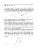
within the elastic region. Load-deflection technique enables measuring E together with σ.
The concept of this technique is shown in figure 1 using a circular membrane. The load-
deflection technique is easy to apply because the membrane is flat without load enabling
Mechanical Properties of MEMS Materials
167
easy load-deflection relationship measurement. The deflection of the membrane center (d) is
measured with the applied pressure (P) across the membrane. Then, the pressure-deflection
behavior of a circular membrane (Tsuchiya, 2008) is expressed by
3
42
0
)1(3
84
d
av
Et
d
a
t
P
−
+=
σ
, (1)
where P is the applied pressure, d is the center deflection, a, t, E, σ
0
and v are the radius,
thickness, Young’s modulus and Poisons ratio of the circular membrane, respectively. As the
equation shows, the range of Poison’s ratio of materials is not wide and rough estimation of
the ratio is acceptable using the bulk properties.
d
p
Thickness t
a
Fig. 1. The load-deflection technique for simultaneous E and σ measurement
2.2 Internal stress
Internal stress (σ), the strain generated in thin films on thick substrates, causes the
deformation of the microstructure and occasionally destruction of the structure. It has two
sources:
- thermal mismatch between a substrate and a thin film – extrinsic stress,
- microscopic structural change of a thin film (caused by chemical reactions, ion
bombardment, absorption, adsorption etc.) – intrinsic stress.
In case of thin film compression the compressive stress is in question. Compressive stress is
expressed as a negative value and it may cause buckling. In case of thin film expansion the
tensile stress is in question. Tensile stress is expressed as a positive value and if excessive
may lead to fracture of structures. According to Hooke’s law, for isotropic materials under
biaxial stress (such as thin films on substrates), internal stress is described by
)1(
ν
ε
σ
−
=
E , (2)
where ε, E and
ν
are the strain, Young’s modulus and Poisson’s ratio of the thin film,
respectively.
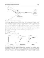
As a micro fabricated test for strain measurement the beam buckling method is often used.
In order to measure ε of thin films the doubly supported beam shown in figure 2 is loaded
by the internal stress. The preparation of pattern with incrementally increasing size enables
determination of the critical length of the beam which causes buckling.
l
w
Fig. 2. Doubly supported beam structure
Micro Electronic and Mechanical Systems
168
The strain deduced from the buckling length of the beam (Tabata, 2006) is given as:
2
2
3
⎟
⎟
⎠
⎞
⎜
⎜
⎝
⎛
=
c
l
t
π
ε
, (3)
where ε, t and l
c
are the strain, thickness of the thin film and the buckling length,
respectively. In this case, the internal stress is assumed to be uniform along the thickness
direction. In case of the stress distribution along the thickness direction, variation of ε may
cause vertical deflection of the cantilever beam.
2.3 Strength
The strength of a material determines how much force can be applied to a MEMS device. It
needs to be evaluated in order to assure reliability of MEMS devices. Strength depends on
the geometry, loading conditions as well as on material properties. As the useful measure
for brittle materials, the fracture strength is defined as the normal stress at the beginning of
fracture. The flexural strength is a measure of the ultimate strength of a specified beam in
bending and it is related to specimen’s size and shape. For inelastic materials, the yield
strength is defined as a specific limiting deviation from initial linearity. The tensile strength
is defined as a maximum stress the material can withstand before complete failure while the
compressive strength is usually related to brittle materials.
2.4 Fatigue
MEMS devices are often exposed to cyclic or constant stress for a long time during
operation. Such operational conditions may induce fatigue. Fatigue may be observed as
change in elastic constants and plastic deformation leading to sensitivity changes and offset
drift in MEMS devices. It may also be observed as the strength decrease that may lead to
fracture and consequentially failure of the device. Fatigue behavior of a MEMS device also
depends on its size, surface effects, effect of the environment such as humidity and
temperature, resonant frequencies etc. In order to realize highly reliable MEMS device a
detailed analysis of the fatigue behavior must be performed using accelerated life test
method as well as life prediction method.
3. Testing methods
Minimum features in MEMS are usually of the order of 1µm. Measuring mechanical
properties of small MEMS specimens is difficult from the aspects of reliability, repeatability
and accuracy of measurements. In order to measure mechanical properties of the MEMS
device a specimen must be obtained and mounted. Since the microdevices are produced
using deposition and etching processes a specimen must be produced by the same process
used in device production. The following step is dimension measurement. The thicknesses
of layers are controlled and measured by the manufacturer and lengths are sufficiently large
to be measured by an optical microscope with required accuracy. However, the width of the
specimen may cause the problem due to its small dimensions as well as imperfect definition
of cross section that may cause uncertainty in the area. Therefore, possible measurement
techniques include optical or scanning electron microscopy, interferometry, mechanical or
optical profilometry. The next step in measuring mechanical properties of MEMS is the
Mechanical Properties of MEMS Materials
169
application of force/displacement resulting in deformation. This step is followed by force,
displacement or strain measurements. Force and displacement measurements are based on
tensile and bending tests or on usage of commercially available force and displacement
transducers. When strain measurements are in question, it is preferable to measure strain
directly on tensile specimens. It enables determination of the entire strain-stress curve from
which the properties are obtained. The strain measurement technique known as
interferometric strain/displacement gage is usually used apart from variety of other
techniques that have not yet been applied to extensive studies of mechanical properties of
MEMS. However, in most cases when MEMS materials are in question, direct methods for
mechanical properties determination are not suitable. Instead, inverse methods are being
used: a model is constructed of the test structure. After the force application and
displacement measurements, elastic, inelastic or strength properties can be extracted from
the model. Nevertheless, the variations in measured properties are large for both types of
testing methods: direct and inverse. The source of variations is not established since there
are too many differences among the properties measured by different methods. Obviously,
the development of international standards for measuring the mechanical properties of
MEMS materials will result in more accurate properties and reliable measurements.
3.1 Tensile testing methods
When tensile testing methods are concerned there are three arrangements that can be used.
The first of them is specimen in a supporting frame. The tensile specimen is patterned onto
the wafer surface and the gage section is exposed by etching the window in the back of the
wafer. The specimen suspended across a rectangular frame enables convenient handling
and testing. An example of specimen in a supporting frame is shown in figure 3.
Fig. 3. Schematic of a silicon carbide tensile specimen in a silicon support frame
The second arrangement used in tensile testing is a specimen fixed at one end. At one end
the test specimens fixed to the die while the other is connected to the test system. There is a
variety of ways a specimen fixed at one end may be connected to a test system. A free end
may be gripped by the electrostatic probe, glued to the force/displacement transducer,
connected to the test system by the pin in case of ring shaped grip end, etc. An example of
specimen fixed at one end is shown in figure 4.
Fig. 4. Schematic of a tensile specimen fixed to the die at one end
The third arrangement used in tensile tests of MEMS materials is the freestanding specimen.
This arrangement applies to small tensile specimens with submillimeter dimensions. The
Micro Electronic and Mechanical Systems
170
geometry commonly used in these tests is shown in figure 5. Microspecimens have grip
ends that can be fitted into inserts in the grips of the test machine.
Fig. 5. Schematic of nickel free standing microspecimen on a silicon substrate
3.2 Bend tests
Similar to tensile testing methods, bend tests also use three arrangements. The first of them
is out-of plane bending. Long, narrow and thin beams of the test material are being
patterned on the substrate. The material under the cantilever beam is being etched away
leaving the beam hanging freely over the edge. By applying the force as shown in figure 6
and measuring the force vs. deflection at the end or near the end of the beam, Young’s
modulus can be extracted.
Fig. 6. Shematic of crystal silicon cantilever microbeam that can be used in out-of-plane
bending test
The second arrangement used in bend tests is the beam with fixed ends – so called fixed-
fixed beam. The schematic of the most usually used on-chip structure is shown in figure 7.
Between the silicon substrate and polysilicon beam with clamped ends a voltage is applied
pulling the beam down. The voltage that causes the beam to make contact is a measure of
beam’s stiffness.
The third arrangement used in bend testing of MEMS materials is in-plane bending (fig. 8).
Test structure consisting of cantilever beams subjecting to in-plane bending may be used in
fracture strain determination, crack growth and fracture toughness measurements, etc.
Fig. 7. Schematic of a polysilicon fixed-fixed beam on a silicon substrate
Mechanical Properties of MEMS Materials
171
Fig. 8. Schematic of polysilicon cantilever beam subjected to in-plane bending
3.3 Resonant structure tests
Resonant structure tests are being used for determination of elastic properties of MEMS
devices. Very small test structures used in these tests can be excited by capacitive comb
drives which require only electrical contact making this approach suitable for on-chip
testing. The most often used resonant structure concepts also include different in-plane
resonant structures with a variety of easily modeled geometries as well as test structures
based on arrays of cantilever beams fixed at one or both ends excited in different manners.
As an illustration, in figure 9 a schematic of a in-plane resonant structure is shown.
Fig. 9. Schematic of the in-plane resonant structure
3.4 Bulge testing
Bulge testing is also often called membrane testing. By etching the substrate material a thin
membrane of test material is formed. The ideal architecture to achieve a direct tensile testing
scheme involves a free standing membrane fixed at both ends (Espinosa, 2003) as shown in
figure 10. When load is applied at the center of the membrane (usually using nanoindenter),
a uniform stretch on the two halves of the thin membrane is achieved. In this manner the
specimen’s structural response is obtained as well as elastic behavior and residual stress
state.
Fig. 10. Shematic of an Au membrane used in bulge testing
3.5 Indentation tests
In indentation tests a miniature and highly sensitive hardness tester (nanoindenter) is being
used allowing force and displacement measurements. Penetration depths can be a few
nanometers deep and automation permits multiple measurements and thus provides more
reliable results. In such a manner Young’s modulus and strength of various thin films can be
obtained. As an illustration, a schematic of an indentation test is given in figure 11.
Micro Electronic and Mechanical Systems
172
Fig. 11. Schematic of indentation test
3.6 Other tests
In order to measure forces in specimens the buckling test method can be used and if the
specimen under pressure breaks the estimate of fracture strength can be obtained. This test
method applied to test structures with different geometries and based on different MEMS
materials can be used for determination of the Poisson’s ratio, strain at fracture, residual
strain in film, etc.
Another test method is the creep test. Creep tests are usually performed in cases when
possibility of creep failure exists such as in thermally actuated MEMS devices resulting in a
strain vs. time creep curve.
When torsion, one of important modes of deformation in some of MEMS devices, is
concerned a few torsion tests have been developed enabling force and deflection
measurements.
Fracture tests are of interest when brittle materials are in question. Fracture toughness is
being measured using crack formation with a tip radius small relative to the specimen
dimensions. Different positions and shapes of cracks are being used formed using different
means such as etching, various types of indenters, etc.
When mechanical testing of MEMS materials is in question, standardization of test methods
is a challenging task. A step forward in the direction of standardization may be
implementation of “round robin” tests that should involve all relevant MEMS researchers in
an effort to test common materials used in MEMS at their premises using the method of
their choice. First such tests resulted in significant variation of results suggesting that further
efforts should be made by involving more scientific resources.
4. Data
Polysilicon is the most frequently used MEMS material. In table 1 polysilicon mechanical
properties data is given obtained by three types of tests: bulge, bend and tensile tests.
Presented results show that polysilicon has Young’s modulus mostly in the range between
160 and 180 GPa. Fracture strength depends on flaws in the material and performed tests do
not necessarily lead to failure of the specimen. For that reason there are fewer entries for
fracture strength and obtained results vary.
Mechanical properties of single-crystal silicon are given in table 2. Presented data is
obtained using bending, tensile and indentation tests. The average values for the Young
modulus ranged between 160 an 190 GPa.
In table 3 silicon-carbide mechanical properties data is presented. It is a promising MEMS
material because of its superior properties (strength, stability, stiffness) and because of the
current work on thin-film manufacturing processes few results are available obtained using
bulge, indentation and bending tests.
Silicon nitride and silicon oxide mechanical properties data is presented in tables 4 and 5,
respectively. Silicon nitride is used as an insulating layer in MEMS devices but it also has a
potential as a structural material. On the other hand, silicon oxide because of its properties
Mechanical Properties of MEMS Materials
173
(low stiffness and strength) although included in MEMS devices does not have a potential of
becoming a MEMS structural material.
There are few reports regarding the mechanical properties of metal thin films. Table 6 lists
measured values of mechanical properties of metal materials commonly used in MEMS
devices: gold, copper, aluminum and titanium. Metal films are tested using tensile testing in
a free-standing manner. Results for electroplated nickel and nickel-iron MEMS materials are
given in table 7. Presented results are obtained using tensile testing methods. Electroplated
nickel and nickel-iron MEMS are usually manufactured by LIGA process. The
microstructure and electrical properties of electroplated nickel are highly dependent on
electroplating conditions while the properties of nickel-iron alloy depend on its
Methods
Young’s Modulus
[GPa]
Fracture Strength
[GPa]
Bulge test 160 -
Bulge test 190-240 -
Bulge test 151-162 -
Bulge test 162±4 -
Bending test - 2.11-2.77
Bending test 170 -
Bending test 174±20 2.8±0.5
Bending test 135±10 -
Bending test 198 -
Bending test - 3.2±0.3
Bending test - 3.4±0.5
Tensile test 164-176 2.86-3.37
Tensile test - 0.57-0.77
Tensile test 140 0.7
Tensile test 160-167 1.08-1.25
Tensile test 169±6 1.20±0.15
Tensile test 132 -
Tensile test 140±14 1.3±0.1
Tensile test 172±7 1.76
Tensile test 167 2.0-2.7
Tensile test 163 2.0-2.8
Tensile test - 1.8-3.7
Tensile test 166±5 1.0±0.1
Tensile test - 4.27±0.61
Tensile test - 2.85±0.40
Tensile test - 3.23±0.25
Tensile test 158±8 1.56±0.25
Tensile test - 2.9±0.5
Fixed ends test 123 -
Fixed ends test 171-176 -
Fixed ends test 149±10 -
Fixed ends test 178±3 -
Table 1. Polysilicon mechanical properties data (Sharpe, 2001)
Micro Electronic and Mechanical Systems
174
composition. Presented results show that these materials have high strength values
(especially Ni-Fe) and therefore are suitable for application in actuators.
In table 8 diamond-like carbon mechanical properties data is presented. Diamond-like
carbon is a MEMS material with excellent properties such as high stiffness and strength and
low coefficient of friction. Presented results are obtained using three types of test methods:
bending, buckling and tensile tests.
Methods
Young’s Modulus
[GPa]
Fracture Strength
[GPa]
Bending test 177±18 2.0-4.3
Bending test 163 >3.4
Bending test 122±2 -
Bending test 173±13 -
Bending test - 0.7-3.0
Bending test 165±20 2-8
Bending test - 2-6
Bending test 169.9 0.5-17
Tensile test 147 0.26-0.82
Tensile test 125-180 1.3-2.1
Tensile test 142±9 1.73
Tensile test - 0.59±0.02
Tensile test 169.2±3.5 0.6-1.2
Tensile test 164.9±4 -
Indentation test 60-200 -
Indentation test 168 -
Table 2. Single-crystal silicon mechanical properties data (Sharpe, 2001)
Methods
Young’s Modulus
[GPa]
Bulge test 394
Bulge test 88±10 - 242±30
Bulge test 331
Indentation test 395
Bending test 470±10
Table 3. Silicon-carbide mechanical properties data (Sharpe, 2001)
Methods
Young’s Modulus
[GPa]
Fracture Strength
[GPa]
Resonant test 130 - 146±20% -
Resonant test 192 -
Resonant test 194.25±1% -
Bulge test 230 & 330 -
Bulge test 110 & 160 0.39-0.42
Bulge test 222±3 -
Indentation test 101-251 -
Indentation test 216±10 -
Table 4. Silicon-nitride mechanical properties data (Sharpe, 2001)
Mechanical Properties of MEMS Materials
175
Methods
Young’s Modulus
[GPa]
Fracture Strength
[GPa]
Indentation test 64 >0.6
Bending test 83 -
Tensile test - 0.6-1.9
Table 5. Silicon-oxide mechanical properties data (Sharpe, 2001)
E
bulk
[GPa]
Young’s
Modulus
[GPa]
Yield
Strength
[GPa]
Ultimate
Strength
[GPa]
Gold 74 98±4 - -
Gold 74 82 - 0.33-0.36
Copper 117 86-137 0.12-0.24 0.33-0.38
Aluminum 69 8-38 - 0.04-0.31
Aluminum 69 40 - 0.15
Titanium 110 96±12 - 0.95±0.15
Table 6. Metal films mechanical properties data (tensile test) (Sharpe, 2001; Tabata, 2006)
Young’s
Modulus
[GPa]
Yield
Strength
[GPa]
Ultimate
Strength
[GPa]
Ni 202 0.4 0.78
Ni 176±30 0.32±0.03 0.55
Ni 131-160 0.28-0.44 0.46-0.76
Ni 231±12 1.55±0.05 2.47±0.07
Ni 181±36 0.33±0.03 0.44±0.04
Ni 158±22 0.32±0.02 0.52±0.02
Ni 182±22 0.42±0.02 0.60±0.01
Ni 156±9 0.44±0.03 -
Ni 160±1 0.28 -
Ni 194 - -
Ni-Fe 119 0.73 1.62
Ni-Fe 155 - 2.26
Ni-Fe - 1.83-2.20 2.26-2.49
Table 7. Electroplated nickel and nickel-iron mechanical properties data (tensile test)
(Sharpe, 2001; Tabata, 2006)
Methods
Young’s Modulus
[GPa]
Fracture Strength
[GPa]
Bending test 600-1100 0.8-1.8
Buckling test 94-128 -
Tensile test - 8.5±1.4
Table 8. Diamond-like carbon mechanical properties data (Sharpe, 2001)
5. Summary
The measurement of MEMS materials mechanical properties is crucial for the design and
evaluation of MEMS devices. Even though a lot of research has been carried out to evaluate
Micro Electronic and Mechanical Systems
176
the repeatability, accuracy and data reliability of various measurement methods for
mechanical properties of MEMS materials, the manufacturing and testing technology for
materials used in MEMS is not fully developed. In this chapter an overview of basic test
methods and mechanical properties of MEMS materials is given along with definitions of
mechanical properties of interest. Also, a summary of the mechanical properties of various
MEMS materials is given. Variation of obtained results for common materials may be
attributed to the lack of international standards on MEMS materials and their properties
measurement methods. It must be pointed out that although MEMS is an area of technology
of rapidly increasing economic importance with anticipated significant growth, the ability to
develop viable MEMS is to a large degree constrained by the lack of international standards
on MEMS materials and their properties measurement methods that would establish
fundamentals of reliability evaluation, especially on MEMS material properties.
6. Acknowledgement
Authors are grateful for the partial support of the Ministry of Science and Technological
Development of Republic of Serbia (contract ТР- 11014).
7. References
Allameh, S.M. (2003). An intorduction to mechanical-properties-related issues in MEMS
structures. Journal of materials science, 38, (2003) 4115-4123, ISSN: 1573-4803
Dual, J.; Simons, G.; Villain, J.; Vollmann, J. & Weippert, C. (2004). Mechanical properties of
MEMS structures, Proceedings of ICEM12, ISBN: 88-386-6273-8, Bari, Italy, August-
September 2004, McGraw-Hill
Espinosa, H.D.; Prorok, B.C. & Fischer, M. (2003). A methodology for determining
mechanical properties of freestanding thin films and MEMS materials. Journal of the
Mechanics and Physics of Solids, 51, (2003) 47-67, ISSN: 0022-5096
Sharpe, W.N.Jr. (2001). Mechanical Properties of MEMS materials, In: The MEMS Handbook,
Mohamed Gad-el-Hak, 3/1– 3/33, CRC Press, ISBN: 978-0849300776, USA
Tabata, O. & Tsuchiya, T. (2006). Material Properties: Measurement and Data, In: MEMS, A
Practical Guide of Design, Analysis, and Applications, Jan Korvink, 53–92, Springer,
ISBN: 978-3540211174
Tsuchiya, T. (2008). Evaluation of Mechanical Properties of MEMS Materials and Their
Standardization. In: Advanced Micro and Nanosystems, Tabata, O. & Tsuchiya, T., 1-
25, Wiley-VCH Verlag GmbH & Co. KgaA, ISBN: 978-3-527-31494-2, Weinheim
Yi, T. & Kim, C-J. (1999). Measurement of mechanical properties for MEMS materials.
Measurement Science and Technology, 10, (1999) 706-716, ISSN: 1361-6501
12
Reliability of MEMS
Ivanka Stanimirović and Zdravko Stanimirović
IRITEL A.D.
Republic of Serbia
1. Introduction
Reliability is a key factor for successful commercialization of micro electronic and
mechanical systems (MEMS). MEMS devices are becoming essential components of modern
engineering systems and their reliability is of particular importance in applications where
their failure can be catastrophic and devastating (surgical devices, implantable biosensors,
navigation in aerospace, sensors in automotive industry, etc.). However, although MEMS
devices are made of minute delicate components realized primarily using physical-chemical
processes, the main reason for the lack of success in commercialization of MEMS cannot be
attributed to the advance of micro technology but to packaging techniques used in
production of MEMS devices. When MEMS packaging is in question, it is of the greatest
importance that design and realization of MEMS device must include all levels of reliability
issues from the onset of the project. For that reason, this chapter is intended to be a general
overview focusing on mechanisms that cause failure of MEMS devices. An insight in
reliability of MEMS packaging (types of MEMS packaging, material requirements and
package reliability) is given. Also, the reliability of MEMS in view of materials, structural
and process reliability and associated failure mechanisms is presented. As the closing
subsection the brief summary of the topic will be presented with an emphasis on the
importance of the further R&D work on MEMS reliability testing and development of
industrial standard for assembly, packaging and testing.
2. Reliability in MEMS packaging
Although the most silicon-based MEMS are produced using the same microfabrication
processes developed for integrated circuits (ICs), these two technologies are significantly
different and MEMS are not evolved integrated circuits. There are several principal
differences between silicon-based MEMS and integrated circuits (Hsu, 2006):
• Silicon–based MEMS are complex 3D structures while integrated circuits are primarily
2D structures.
• Many MEMS devices involve precision movement of solid components and fluids in
sealed enclosures, and integrated circuits are stationary encapsulated electric circuits.
• While MEMS perform a great variety of specific functions of biological, chemical,
electromechanical and optical nature, integrated circuits transmit electricity for specific
electrical functions.
Micro Electronic and Mechanical Systems
178
• MEMS as delicate moving or stationary components are interfaced with working media
while IC dies are isolated from contacting media.
• MEMS are using silicon and silicon compounds plus variety of other industrial
materials, while integrated circuits are limited to single crystal silicon and silicon
compounds, ceramic and plastic.
• In MEMS there are many components to be assembled and in integrated circuits there
are fewer components to be assembled.
• MEMS packaging technology is far from being developed while IC packaging
techniques are relatively well developed.
• For MEMS there are no available industrial standards regarding design, materials
selections, fabrication processes and assembly-packaging-testing while integrated
circuits have available industrial standards in all these areas.
• Most MEMS are custom built and assembled on batch production lines in contrast to
mass production of ICs.
• MEMS have limited sources of commercialization while integrated circuits are fully
commercialized.
MEMS packaging is more complex than packaging of integrated circuits because of their
complex structures and specific performances. MEMS packaging must provide support and
protection to ICs, associate wire bonds and the printed circuit board (PCB) from mechanical
or environmentally induced damages and protect elements that require interface with
working media which can be environmentally hostile. The fact that many MEMS require
non-standard packages is one of the reasons why they have not made their way to the
market. There are three basic types of packages used in MEMS technology: ceramic, metal
and plastic. Some of the features of these three types of packages are given in table 1.
2.1 Materials selection for MEMS packaging
When MEMS devices are in question, materials selection should be done carefully. Similar
to IC packaging, most of the MEMS devices are diced from a wafer and mounted on a
substrate inside a package and therefore a careful attention must be paid to die attachment
materials selection. Die attach material should firmly bond die to the substrate eliminating
any possibility of motion. Die movement may cause various problems especially in
optoelectronic devices where alignment is important. Fracture toughness is very important
for brittle attachment materials because it determines material resistance to fracture.
Mismatch of the coefficient of thermal expansion (CTE) between die attach material, silicon
and substrate may lead to undesirable stress. Another important factor in attachment
materials selection is thermal conductivity because die attachment material conducts heat
from the die to the substrate. Moisture adsorption is critical because it causes degradation of
die attach bonding properties. In order to minimize stress induced to the die, organic
materials (epoxies, silicones, polyamides) are often used as die attach materials. These low
cost materials are also convenient because of the ease of rework. However, in unpassivated
MEMS devices outgassing of organic material may cause contamination. Organic materials
are usually not used for ceramic packages. Temperature needed to produce frit seal after die
attachment may lead to the degradation of the adhesive. Inorganic materials are also being
used as die attach materials. These materials exhibit excellent fatigue resistance and provide
lowest levels of contaminant gasses, but due to the lack of plastic flow may cause mismatch
between substrate and die.
Reliability of MEMS
179
Ceramic packaging
• Commonly used in MEMS packaging
• Usually consist of a base and a header
• Die attachment by solder or adhesives
• Generally electrically insulating
• Hermetic
• The match between coefficient of linear
thermal expansion between ceramic and
Si is fairly good
• High mechanical strength
• Resistant to chemicals
Metal packaging
• Robust
• Easy to assemble
• Allow prototyping in small volumes with
short turnaround periods
• Hermetic when sealed
Plastic packaging
• Cost effective
• Small weight
• Allow moist absorption
Table 1. Main features of three basic types of packages used in MEMS technology
Substrates for MEMS packaging must meet different electrical, thermal, physical and
chemical requirements. One of the most important factors is dielectric constant of the
substrate whose high value may cause crosstalk between wires. Another important factor is
CTE. In order to minimize the thermal-mechanical stress in the package that may cause
cracks or errors (in piezo-resistive sensor elements), CTE values of the substrate, die and die
attach material must be matched. Another substrate property that must be taken into
consideration is the loss tangent. If the substrate with high loss tangent is used,
performances of MEMS devices sensitive to the frequency of applied signals may be
reduced significantly. That also may result in low quality factor (Q) which measures
performances of MEMS devices. Thermal conductivity of the substrate is important from the
aspect of the heat transfer and porosity. Also, porosity and purity of the substrate must be
evaluated because of the possibility of moisture penetration through the substrate.
Properties of most commonly used substrates for MEMS packaging are given in table 2. It
should be pointed out that Low Temperature Cofired Ceramic (LTCC) being the multilayer
substrate allows implementation of cavities and allows movement in Z direction.
2.2 MEMS package reliability
When MEMS package reliability is in question, basic issues that should be taken into
consideration are issues related to reliability of die attachments, ceramic substrates and
released MEMS structures.
Mechanical connection between the substrate and MEMS structure is provided by die attach
materials. CTE mismatch between used materials induces stress on the MEMS structure that
may lead to formation of cracks on silicon MEMS structure. Cracks can appear at the centre
or at the corners of the die usually when hard adhesives are used as die attach materials. In
that case, CTE mismatch stress is transferred to the die causing cracks. Die attach can also
crack if soft adhesives are used because it acts as a strain buffer at the die-substrate interface.
Micro Electronic and Mechanical Systems
180
Single Layer
Substrates
Tensile
Strength
(MPa)
Elastic
Modulus
(GPa)
Flexural
Strength
(MPa)
Dielectric
Strength
(kV/mm)
BeO 230 345 250 0.78
Si - 310-343 360 0.55
AlN - 190 580 -
Al
2
O
3
(96%) 127.4 310.3 317 0.33
Al
2
O
3
(96%) 206.9 345 345 0.33
Steatite 55.2-69 90-103 110 7.9-15.7
Fosforite 55.2-69 90-103 124 7.9-11.8
Quartz 48.3 71.7 - -
Single Layer
Substrates
Dielectric
Constant
@ 1MHz
Thermal
Conductivity
(W/m°C)
CTE
(ppm/°C)
BeO 6.7-8.9 150-300 6.3-7.5
Si 8.5-10 82-320 4.3-4.7
AlN 11.9 125-148 2.33
Al
2
O
3
(96%) 4.5-10 15-33 4.3-7.4
Al
2
O
3
(99%) 4.5-10 15-33 4.3-7.4
Steatite 5.5-7.5 2.1-2.5 8.6-10.5
Fosforite 6.2 2.1-4.2 11
Quartz 4.6 43 1.0-5.5
Multilayer Substrate
LTCC 6-9 2-4 5-7
Table 2. Properties of commonly used substrates for MEMS packaging (Pecht, 1998)
When organic die attach materials are being used, outgassing becomes an issue. In that case
vacuum packaging is recommended. It protects MEMS devices from damage and
contamination. Besides outgassing, if the organic die attach material is being used, moist
absorption may cause failure. In hermetically sealed packages moisture trapping may occur
causing delamination.
When ceramic substrate reliability is in question, CTE mismatch between substrate and
silicon die may induce stress on the die causing cracking or bending. This can be avoided by
careful evaluation of material properties. Matching CTE values of the substrate and the die
lead to elimination of this problem.
Another reliability issue when MEMS package reliability is in question is packaging of
released MEMS structures. Since they are susceptible to contamination, excessive handling,
mechanical shock and stiction caused by the presence of moisture, the wafer level vacuum
packaging is recommended.
3. Reliability of MEMS
Variety of applications may lead to misconception that amount of different structural parts
of MEMS devices is large. However, there are a number of basic parts that are being used:
cantilever beams, membranes, hinges, etc. The most common generic MEMS elements are
listed in table 3.
Reliability of MEMS
181
• Structural beams
• rigid
• flexible
• one side clamped
• two sides clamped
• Structural thin membranes
• rigid
• flexible
• with holes
• Flat layers (usually adhered to substrate)
• conductive
• insulating
• Hinges
• substrate hinge
• scissors hinge
• Cavities
• sealed
• open
• Gears
• teeth
• hubs
• Tunnelling tips
• Reflective layers
Table 3. Generic MEMS elements (Merlijn van Spengen, 2003)
MEMS devices are usually batch fabricated using silicon wafers as the material and etching
techniques to build components. Fabrication process is more complex than fabrication
process of ICs because of mechanical parts and electromechanical parts that are being
integrated with electronic parts on the same substrate. MEMS have more complex shapes,
have moving parts and need more material strength. Mechanical parts need special
attention throughout the production cycle: from material deposition to material removal.
These parts may have complex shapes, may require material with special strength and may
have moving parts. Therefore, deposited film must be thick enough to form the mechanical
layer. Moving parts are released after etching away the SiO
2
layer. Common processing
techniques include bulk micromachining, wafer-to wafer bonding, surface micromachining
and high-aspect ratio micromachining. Many MEMS failure modes are introduced in the
fabrication process. Also, many failure modes in operation are related to fabrication process.
MEMS common failure modes are fracture, creep, stiction, electromigration, wear,
degradation of dielectrics, delamination, contamination, pitting of contacting surfaces,
electrostatic discharge (ESD), etc.
One of the most important failure modes is stiction. Due to small sizes of MEMS structures
surface forces dominate all others. The most important surface forces in MEMS are
electrostatic force, capillary force and molecular van der Waals force (Tadigadapa, 2001).
They cause stiction between microscopic structures when their surfaces come into contact. It
can affect even elements that are not powered. Illustration of this failure mode is given in
figure 1.
Micro Electronic and Mechanical Systems
182
Fig. 1. Illustration of stiction failure mode
Creep is important issue for reliability of metal MEMS. High stresses and stress gradients
introduce possibility of time-dependent mass transfer through glide and diffusion
mechanisms. The creep is much more severe in MEMS structures than expected from
macroscopically known behaviour. Macroscopically, creep is negligible. MEMS
manufacturers should pay special attention when using metal as a structural material in
MEMS where room temperature creep exists.
Most metals and alloys are degraded by material fatigue when subjected to a large repetitive
mechanical stress. Cyclic loading of MEMS couples with other failure mechanisms
associated with static loading, creep and environmental effects. Any process that results in
an irreversible repositioning of atoms within a material can contribute to fatigue. Brittle
materials like ceramics and silicon do not have a significant cyclic fatigue effect. Poly and
possibly mono-crystalline silicon seem to suffer from a stress corrosion cracking mechanism
(Muhlstein, 1997). In a not completely water free environment, small cracks propagate
under tensile stress, due to hydrolysis of the native oxide layer (fig.2).
Si
Si
O
2
Initial crac
k
Propagation
FF
Fracture
FF
Fig. 2. Stress corrosion cracking failure mechanism
Friction and wear are of interest when sliding/rotating MEMS are in question. The wear
mechanism in silicon is adhesive wear (Merlijn van Spengen, 2003). Rough contacting
surfaces adhere to each other at their highest points. These points are broken and stay
attached to other surfaces. Material is then transferred between surfaces and when asperities
grow to a certain size they break off leaving worn surface and causing the accumulation of
debris. Illustration of adhesive wear is shown in figure 3.
FF
FF
Fig. 3. Illustration of adhesive wear
Dielectric charging is an important issue for reliability of MEMS that contain dielectric layers.
Parasitic charge accumulating in MEMS may alter actuation voltages and affect mechanical
Reliability of MEMS
183
behavior of the device. Also, a common problem is charging due to high field strengths
required for actuation of electrostatically actuated MEMS.
Delamination is associated with multilayer films. High stress can be introduced by
processing, thermal mismatch or epitaxial mismatch. The adhesion between layers depends
strongly on their chemical and mechanical compatibility.
Electrostatic clamping of gears may prevent gears from moving due to presence of electrical
charges at certain energy levels.
Particles have a damaging effect on devices where small gaps exist between bearing surfaces
or elements with large potential difference. Particulate contamination is important when
contaminating particles are internally generated or present in spite of a clean room
environment.
Environmental effects may be important for design of variety of MEMS applications.
Environmental Attack is of interest in case of valves, sensors and pumps where contacting
fluids may be corrosive resulting in crack growth.
MEMS failure mechanisms are numerous and list of possible failure modes does not end
here. Root causes of MEMS failure modes are different from the common causes on
macroscopic level. Some of them are capillary forces, operational methods, mechanical and
electrical instabilities. MEMS failure analysis techniques are similar to techniques that are
being applied in failure analysis of ICs: optical microscopy, scanning laser microscopy,
scanning electron microscopy, focused ion beam, atomic force microscopy, light emission,
acoustic microscopy, acoustic emission, laser cutting, lift-off technique, etc. Failure models
for MEMS are scarce because a failure model should be able to describe physic of failure and
allow failure prediction. It is obvious that current knowledge of MEMS reliability is
insufficient in comparison with the amount of MEMS devices that are already available.
4. Conclusion
An insight in reliability of MEMS packaging and the reliability of MEMS has been presented
in this chapter. Since there is a common misconception that silicon MEMS devices and ICs
are similar because they use the same microfabrication techniques, principal differences
between silicon-based MEMS and ICs have been outlined. Materials selection for MEMS
packaging has been considered as well as MEMS package reliability. As far as MEMS
generic elements are concerned, a number of common failure modes have been presented.
Reliability of MEMS devices requires better understanding of mechanisms that cause failure
in MEMS devices. Production of reliable MEMS device requires sophisticated design
considerations and better control of microfabrication processes that are used in production
and packaging of a MEMS device. Reliable MEMS package should isolate non-sensing areas
from sensing ones what is of extreme importance in harsh, corrosive or mechanically
demanding environments. Also, it must not prevent mechanical action of moving parts of
the structure or disable transfer of fluids from one region to another. Coupling of energy,
motion or momentum from one region to another should be allowed. Finally, reliable
MEMS package should prevent transfer of heat, mechanical strain, outgassing, pressure,
moisture, etc. Reliability of MEMS generic elements is also of utmost importance.
Knowledge of physics of degradation and failure mechanisms in the microdomain is still
very limited. Another important issue is the need for credible testing techniques to be used
during fabrication, assembly and packaging as well as during operation of the device.
Device with self-testing capability will insure the reliability of the device during service.
Micro Electronic and Mechanical Systems
184
It should be pointed out that little research and development efforts have been made in the
area of testing. MEMS reliability studies lack dedicated equipment and the development of
new and the upgrading of existing equipment is highly desirable. Also, highly diversified
functions and materials involved make industrial standard for MEMS packaging almost
impossible task. Projected timeline for standardization of MEMS technology is at least five
years away (Hsu, 2006). Till then MEMS devices will be custom made according to
customer’s requirements and the lack of information flow as well as the reluctance in
sharing experience and knowledge will keep MEMS still far away from the full
commercialization.
5. Acknowledgement
Authors are grateful for the partial support of the Ministry of Science and Technological
Development of Republic of Serbia (contract ТР- 11014).
6. References
Hsu, T-R. (2006). Reliability in MEMS packaging, Proceedings of 44
th
International Reliability
Physics Symposium, ISBN: 0-7803-9498-4, San Jose, CA, March 26-30, 2006, IEEE
International
Merlijn van Spengen, W. (2003). MEMS reliability from a failure mechanisms perspective.
Microelectronics Reliability, 43, 7, (2003) 1049-1060, ISSN: 0026-2714
Muhlstein, C. & Brown, S. (1997). Reliability and Fatigue testing of MEMS, In:
NSF/AFOSR/ASME Workshop, Tribology Issues and Opportunities in MEMS, Bhushan,
B. pp. 519- 528, Springer, ISBN: 0792350243
Pecht, M.G.; Agarwal, R.; McCluskey, P.; Dishongh,T.; Javadpour, S. & Mahajan, R.(1998).
Electronic Packaging Materials and Their Properties, CRC Press, ISBN: 978-
0849396250, USA
Tadigadapa, S. & Najafi, N. (2001). Reliability of Microelectromechanical Systems (MEMS),
Proceedings of Reliability, Testing, and Characterisation of MEMS/MOEMS Conference,
pp. 197-205, ISBN: 0-8194-4286-0, San Francisco, CA, October 22-24 2001, SPIE,
Bellingham, USA
13
Numerical Simulation of Plasma-Chemical
Processing Semiconductors
Yurii N. Grigoryev and Aleksey G. Gorobchuk
Institute of Computational Technologies Russian Academy of Sciences, Siberian Branch
Russia
1. Introduction
The growing rates of microchip world production during the last two decades exceed
essentially the corresponding indexes of any others production branches. Between 1997 and
2003 the consumer and communication electronics sales have grown from USD 744 billion to
about USD 165 trillion. The present-day electronics is based on a silicon technology and
such a state will be conserve at least during the nearest ten years. The low temperature
plasma facilities - so called plasma reactors or glow discharge reactors, play an important
role in technological processes of chip production.
Such reactors are widely used for etching and deposition of semiconductor films, for taking
off photoresist and some other operations. Very often they enter the complex cluster
equipment for making chips.
Some characteristic schemes of these glow discharge reactors are presented in Fig. 1. The
typical reactor consists of two parallel plate electrodes forming an axisymmetrical cylinder
chamber, in which the high-frequency discharge is appeared. The processing wafer is placed
on one of the electrodes. The originally inert feed gas enters the discharge zone where an
active etchant species is produced by the electron - impact dissociation. The active species
transfers to the wafer and reacts with it forming the volatile products. The unreacted feed
gas and the products of physical-chemical processes and reactions are pumped outwards
from the reactor.
From the presented schemes one can see that these reactors are not very complicated and
expensive apparatus. But yet in 1995 a world volume of sales of the reactors have made up
USD 2 billion and it keeps on growing. This numeral can give us a rough idea about the
quantity of operative reactors in modern industry.
Despite of the relative simple construction the etching process in a reactor is a very
complicative one. For silicon wafer operating the complex molecular gases such as CF
4
, SF
6
and their mixtures with oxygen O
2
and hydrogen H
2
are used. Under a microwave
discharge and ion current in etching chamber a reacting medium appears which is
characterized by simultaneously proceeding processes of ionization, dissociation, heat and
mass transfer with complex chemical reactions. A similar processes take place on the
surfaces of the chamber and wafer under operating.
The quality and manufacturing rate of producing chips depend strongly on a large number
of process variables in a reactor including parent gas composition, pressure, temperature,
frequency and power of a discharge, flow rate and configuration, etc. Because of numerous
Micro Electronic and Mechanical Systems
186
and complex interconnections of the factors which defines the qualities of etching wafer, the
opportunities of experimental studies and optimization of reactor process are very
restricted.
Fig. 1. The schemes of plasma - chemical etching reactors: a – “pedestal”, b – “stadium”, c -
radial flow reactor. 1, 2 - RF - electrodes, 3 - processing wafer, 4 - protector, 5 - feed gas, 6 -
RF - discharge zone, 7 - inlet, 8 - outlet. The arrowed lines show the direction of the gas flow
in the reactor.
A natural alternative here is the mathematical modelling. It is especially necessary in respect
to insufficient understanding of many real plasma physics and chemistry governing
mechanisms which take place in this apparatus.
Numerical Simulation of Plasma-Chemical Processing Semiconductors
187
By such a way there are economical, technical and scientific preconditions for the well-
directed efforts in the development of mathematical modelling of plasma etching reactors.
2. Numerical model formulation
In first turn some characteristic features of authors' numerical model of plasma etching
process will be described. The numerical model was developed during several years with
successive improving its adequacy and prognostic abilities step by step (Grigoryev &
Gorobchuk, 1996; Grigoryev & Gorobchuk, 1997; Grigoryev & Gorobchuk, 1998; Shokin et
al., 1999; Grigoryev & Gorobchuk, 2004; Grigoryev & Gorobchuk, 2007; Grigoryev &
Gorobchuk, 2008). Today the created model corresponds completely to the world standards
in mathematical modelling of plasma reactors and includes some novel elements.
2.1 Gas flow and temperature distribution
Under the typical operating conditions in plasma reactors the continuum approach is valid,
and gas flow is laminar, viscous and incompressible. Therefore, the steady Navier - Stokes
equations with heat transfer in standard Boussinesq approximation were used for the flow
description (Grigoryev & Gorobchuk, 1997; Grigoryev & Gorobchuk, 1998; Shokin at al.,
1999). The axisymmetric statement of a problem is considered. The conservation equation of
total mass (continuity equation) was written as follows:
0
∇
⋅=v (1)
The conservation equation of momentum had the form:
000
*
(),
[()]
TT
p
ρτρβ
τη
⋅∇ =∇⋅ − −
=− + ∇ + ∇
vv g
Ivv
(2)
where
ρ
is a density of gas mixture, v is a fluid velocity vector, p is a pressure,
τ
is a stress
tensor, I is a identity matrix, T is a local temperature of gas mixture, T
0
is a temperature of
the feed gas at the inlet of the reactor, g is a gravitational acceleration vector,
β
is a thermal
expansion coefficient,
η
is a shear viscosity. The density
ρ
0
corresponds to the gas
temperature T
0
. For the velocity components on impenetrable walls the nonslip boundary
conditions were used in range of operating pressures p = 0.1 – 1.0 torr and slip conditions for
low pressures p = 0.01 – 0.1 torr correspondingly.
The temperature distribution was obtained by solving the energy balance equation with
heat transfer at the surfaces of reactors (Grigoryev & Gorobchuk, 1997; Grigoryev &
Gorobchuk, 1998; Shokin et al., 1999):
()() ,
p
r
cT T
ρ
λ
⋅
∇ =∇⋅ ∇ −∇⋅vq (3)
where c
p
is a constant - pressure heat capacity,
λ
is a gas thermal conductivity, q
r
is a
radiation flow rate. The radiation flow
r
q under operating pressures p = 0.1-1.0 torr was
calculated in thin optical layer approximation.
The dynamical and energy balance equations were coupled through the temperature
dependence of gas viscosity and the buoyancy term. The gas viscosity, thermal conductivity
and heat capacity were considered as functions of temperature. The boundary conditions on
the temperature expressed a balance of convective flow, heat conduction and radiation heat
Micro Electronic and Mechanical Systems
188
flows at the solid walls. At the axis of symmetry the no flux boundary condition was used.
The gas temperature at the inlet of reactor is equal to the wall temperature. Under low
pressures a “temperature jump” condition was used.
2.2 Physical-chemical kinetics and species concentration distribution
In general case a binary mixture CF
4
/O
2
was considered as a parent gas because it is widely
spread in silicon technology (Grigoryev & Gorobchuk, 2004; Grigoryev & Gorobchuk, 2007).
An important difficulty for CF
4
/O
2
system is a simulation of plasma-chemical kinetics
which is extraordinarily complicated. Generally the governing set of chemical reactions and
corresponding number of reagents essential for given chemical system are chosen using real
experimental data. For Si - CF
4
/O
2
parent system a subset of 14 gas-phase reactions were
derived which describes adequately the experimental observations (Plumb & Ryan, 1986).
This improved chemical kinetic model was added by several heterogeneous reactions with
CF
2
, CF
3
radicals (Venkatesan at al., 1990; Sang-Kyu Park & Economou, 1991).
The kinetic model included the following processes: electron-impact dissociation of binary
gas mixture, volume recombination of reactive atoms and radicals, silicon etching,
chemisorption of fluorine and oxygen atoms on Si surface, recombination and adsorption of
CF
2
, CF
3
at wafer. The complete set of reactions used in the paper looks as follows:
1
43
CF CF F ,
k
e
ee
−
−
+→ ++ (4)
2
42
CF CF 2F ,
k
e
ee
−
−
+→ ++ (5)
3
2
OOO,
k
e
ee
−
−
+→ ++ (6)
4
2
COF COF F ,
k
e
ee
−
−
+→ ++ (7)
5
2
CO CO O ,
k
e
ee
−
−
+→ ++ (8)
1
33 26
CF CF C F ,
k
v
M
M++→ + (9)
2
34
FCF CF ,
k
v
M
M++→ + (10)
3
23
FCF CF ,
k
v
M
M++→ + (11)
4
32
OCF COF F,
k
v
+
→+ (12)
5
2
OCF COFF,
k
v
+
→+
(13)
6
2
OCF CO2F,
k
v
+→ + (14)
7
2
OCOF CO F,
k
v
+
→+ (15)
Numerical Simulation of Plasma-Chemical Processing Semiconductors
189
8
2
FCOF COF ,
k
v
M
M++→ + (16)
9
FCO COF ,
k
v
M
M++→ + (17)
10
2
FF F ,
k
v
M
M++ → + (18)
11
2
FFF,
k
v
M
M+→ ++ (19)
1
33
CF CF ( ),
k
s
s
→ (20)
2
22
CF CF ( ),
k
s
s
→ (21)
3
23
FCF () CF,
k
s
s+→ (22)
4
34
FCF () CF,
k
s
s+→ (23)
5
33 26
CF CF ( ) C F ,
k
s
s+→ (24)
6
2
CF ( ) O CO 2F,
k
s
s +→ + (25)
7
3
CF ( ) O CO 3F,
k
s
s +→ + (26)
8
OO (),
k
s
s
→ (27)
9
O ( ) F O F,
k
s
s
+
→+ (28)
4
4F Si SiF ,
k
s
+
→↑ (29)
4
4F Si I SiF .
k
i
+
+
+→ ↑ (30)
where k
e1
-k
e5
are the rate constants of electron-impact dissociation of parent gas; k
v1
-k
v11
are
the rate constants of volume recombination; k
s1
-k
s7
are the rate constants of heterogeneous
reactions. The designation (s) marks the species adsorbed on the wafer surface. The values
of these constants were taken from (Plumb & Ryan, 1986; Venkatesan at al., 1990; Sang-Kyu
Park & Economou, 1991).
The model contains 16 gas-phase reactions and 8 heterogeneous reactions on the wafer.
Reactions Eqs. (4)-(8) represent the electron-impact dissociation of binary gas mixture; Eqs.
(9)-(19) are the reactions of volume recombination of reactive atoms and radicals; Eqs. (20)-
(26) are the reactions of recombination and adsorption of CF
2
, CF
3
at wafer; Eqs. (27), (28)
are the chemisorption processes of fluorine and oxygen atoms on Si surface; Eqs. (29), (30)
are the reactions of spontaneous and ion-induced silicon etching correspondingly. The
Micro Electronic and Mechanical Systems
190
twelve products of dissociation and recombination processes - F, F
2
, CF
2
, CF
3
, CF
4
, C
2
F
6
, O,
O
2
, CO, CO
2
, COF, COF
2
are taken into account.
Accordingly to multicomponent chemical kinetic model the distribution of species
concentration for each component was derived from the system of convective-diffusion
equations:
= ( ( ln )) ( , ), , = 1, ,12,
itiiT iij
CCDxkTGCCij
⋅
∇∇⋅ ∇+∇ +v … (31)
where C
i
, x
i
are the molar concentration and molar fraction of species i correspondingly,
t
C
is the molar gas concentration, D
i
is the multicomponent diffusion coefficient of species i, k
T
is the thermal diffusion relation, G
i
is the rate of formation of species i in gas-phase
reactions. The gas phase reactions are incorporated in right-hand side of this system and
define a complex interconnection between all species generation processes. The surface and
silicon etching reactions entered the boundary conditions at the wafer. The latter were
written as a balance of mass flows for each component. At the reactor inlet the Danckwert's
type boundary conditions were stated (Sang-Kyu Park & Economou, 1991). The feed species
concentrations at the inlet are fixed. No radial gradients of species concentrations are
considered at the reactor centerline. At the reactor outlet, zero axial gradients of species
concentrations are also used.
2.3 Glow discharge structure and electron concentration
The exact calculation of glow discharge structure demands a solving the Boltzmann kinetic
equation for the electrons in a mixture multiatomic gases and radicals. From both physical
and computational points of view this is a formidable task (Aydil at al., 1993). Therefore in
the parametric calculations some simplest model distributions of electron density in reactor
were used. Depending on the pressure and gas medium under consideration, the dominant
electron loss mechanism can be diffusion, recombination or attachment. In calculations
usually it was assumed that the electron density distribution corresponded to a “diffusion-
dominated” discharge (Dalvie at al. 1986).
2.4 Numerical method
The presence of two-order elliptic operators in all equations of the mathematical model
allows us to approximate each equation by implicit iterative finite difference splitting-up
scheme with stabilizing correction (Grigoryev & Gorobchuk, 1996). The scheme in general
form looks as follows:
).(
),(
1
2/11
1
2/1
kk
z
kk
kk
z
k
r
kk
L
FLL
φφ
τ
φφ
φφφ
τ
φφ
φ
φφ
−=
−
++=
−
+
++
+
+
The scheme has
22
12
()Ohh
τ
++ approximation order where
12
,hh are the mesh sizes along r
and z coordinates,
τ
is the iterative parameter. The solution of the original steady state
problem was derived by the relaxation method. The iterative process was terminated after
achieving the relative error
10 4
10 10
φ
ε
−
−
=− in the uniform norm