Micro Electronic and Mechanical Systems 2009 Part 10 ppt
Bạn đang xem bản rút gọn của tài liệu. Xem và tải ngay bản đầy đủ của tài liệu tại đây (3.97 MB, 35 trang )
Micro Electronic and Mechanical Systems
306
Pd/SiC contact at 700
0
C initializes dissociation of SiC surface in the presence of Pd atoms.
The released Si atoms interact with palladium to form palladium silicide while the dissolved
carbon atoms start to accumulate at the interface. The XPS spectra have established the
presence of the two palladium silicides Pd
3
Si and Pd
2
Si together with carbon in graphite
state distributed in the whole contact film. As a result, the SiC interface is shifted into the
SiC bulk, since a part of the original interface is consumed to supply Si for the Pd
3
Si
formation. After annealing of the Au/Pd/Ti/Pd contact, a new contact composition has
been obtained. The contact layer consists of Au in a metal state, unreacted Pd, palladium
rich silicide (Pd
3
Si) and TiC, while the interface layer is composed of a less Pd-rich silicide
(Pd
2
Si). As in the Pd/SiC contact a part of the original interface is consumed due to the
partial dissociation of SiC to Si and C. Again, the free Si atoms interact with Pd to form Pd
2
Si
in the interface near region and Pd
3
Si in the more remote contact layer, while the dissolved
C atoms react with Ti and TiC is formed. Due to the presence of Ti in the contact
composition, the carbon resulting from SiC dissociation during annealing is completely
consumed. It should be noted that in contrast to the Pd/SiC contact, no carbon in graphite
state has been observed in the annealed Au/Pd/Ti/Pd contact. The absence of free C in the
annealed contact causes improvement of the contact stability during the long-term
treatments and at high operating temperatures. The presence of Au and Pd in metal state
contributes to the good contact conductivity.
Fig. 11. XPS depth profiles of Pd-based contacts: a) Pd/SiC annealed at 700
0
C and
(b) Au/Pd/Ti/Pd/SiC annealed at 900
0
C.
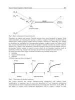
3.3 Thermal stability of n- and p-type ohmic contacts to SiC.
By contrast with the Si and GaAs devices, which operating temperature is limited by the
electronic properties of the semiconductor material, the maximum operating temperature of
SiC and III-nitride devices is limited by stability of the contacts. Some device parameters
such as response time, output power and etc. depend strongly on the ohmic contact
resistivity and its stability at high operating temperatures. Therefore the contact reliability
at high temperature treatment is considered as the critical factor determining their power
application.
The thermal stability of the contacts consists in their parameters remaining unchanged
under the effect of the temperature. This property is investigated on the basis of the
behaviour of a physical or electrical parameter characterising the contact under the effect of
the temperature. For ohmic contacts such parameter is the resistivity. Usually, the thermal
stability of ohmic contacts is investigated for long time treatment at fixed temperatures
Ohmic Contacts for High Power and High Temperature Microelectronics
307
(ageing test) and by the dependence of the resistivity on the dynamically increasing
temperature (temperature-dependence test).
In this section the thermal properties of Ni-based, Al-based and Pd-based ohmic contacts to
SiC are presented (Kakanakov et al., 2004; Kolaklieva et al., 2004; Kassamakova-Kolaklieva
et al., 2003). The effect of the long term ageing of the contacts on the electrical properties has
been studied by heating at 500
0
C, 600
0
C and 700
0
C for 100 hours at each temperature. In
fixed time intervals the contacts are cooled to room temperature and the contact resistivity is
measured. The results from this study are summarized in Fig.12. All contacts show non-
essential change of the resistivity during 100 hours ageing at 500
0
C. Both Pd-based contact
types have demonstrated good thermal stability at 500
0
C heating for 100 hours. Increase of
the ageing temperature to 600
0
C results in different contact behaviour. A significant effect
of the thermal treatment at this temperature is observed on the electrical properties of the
Au/Pd contacts. After 24 hours heating their contact resistivity increases to a value of
1.4x10
-4
Ω.cm2. Further heating at this temperature does not deteriorate them. On the
contrary, the Au/Pd/Ti/Pd contacts show excellent thermal stability during ageing at 600
0C and 700 0C. The improved thermal stability of Au/Pd/Ti/Pd ohmic contacts can be
explained by formation of a thermodynamically stable contact configuration during
annealing. The annealing of the Au/Pd contacts results in formation of Pd
2
Si at the
interface. Pd
2
Si is the Pd-richest silicide, which is in thermodynamic equilibrium with SiC.
Therefore it is considered as a metallization to SiC stable during prolonged thermal
treatments. However, the formation of palladium silicides during annealing leads to the
accumulation of free C within the contact layer, which is responsible for the observed
instability of Au/Pd contacts during the long term ageing at higher temperatures. During
annealing of the Au/Pd/Ti/Pd contacts two processes run: formation of Pd
2
Si at the
interface and reaction between the titanium and the free carbon in the contact layer. The
latter leads to the formation of the thermodynamically stable TiC compound phase and
reduction (or total use up) of the free C in the contact layer, which results in improving of
the thermal stability of the contacts.
Fig. 12. Dependence of the contact resistivity on the long-term temperature treatment of: (a)
Ni-based and Pd-based contacts, and (b) Al-based contacts.
Increase of the ageing temperature to 600
0
C causes a very small rise of the resistivity of the
Au/Al/Si contact. The resistivity of both contacts, Au/AlSiTi and Au/Ti/Al, remain
Micro Electronic and Mechanical Systems
308
practically the same during the whole time interval at this temperature. During heating at
700
0
C, the Au/Al/Si contact resistivity increases continuously to a value of 6.4x10
-4
Ω.cm2
measured after the 100th hour. Slight increase of the resistivity from 9.1x10⁻⁵ Ω.cm2 to
1.2x10⁻⁴ Ω.cm2 is noticed for the Au/AlSiTi contact with the same test. No practical changes
in the contact resistivity are detected when the Au/Ti/Al contact is subjected to ageing at
700 0C for 100 hours. The addition of Ti to the contact composition improves its thermal
and power properties. This effect is less pronounced in the Au/AlSiTi contacts because of
the very small Ti amount in the contact composition. Due to the higher Ti concentration the
carbon resulted from the SiC dissociation during annealing is completely consumed and TiC
is formed in the contact layer. The absence of C in graphite state is the main factor, which
ensures the stability of Au/Ti/Al contact during the ageing up to 700 0C.
The resistivity of Ni-based contacts remains practically the same in the whole time interval
at these temperatures. Small instability has been observed with Au/Ni contacts after ageing
at 600
0
C, but the resistivity remains still low. The observed excellent thermal stability of
these contacts is due to the formation of the chemically stable interface with the
semiconductor and a stable contact composition of Ni
2
Si.
In the temperature-dependence test the measurements have been proceeded at a
temperature increasing smoothly from 25
0
C to 450
0
C in air. This study gives information
on the contact reliability at the corresponding operating temperature as the contact
resistivity has been measured during the heating. For the temperature-current treatment, a
current with a pre-set density of 10
3
A/cm
2
is supplied for a fixed time at a constant
temperature (up to 450
0
C). This test has been also performed in air and contact resistivity is
measured at the corresponding temperature. The results from the two tests are presented in
Fig. 13.
Fig. 13. Dependence of the contact resistivity on the operating temperature and supplied
power of: (a) Ni-based and Pd-based contacts, and (b) Al-based contacts
Au/Pd/Ti/Pd contacts have demonstrated better stability at operating temperatures in the
interval 25
0
C – 450
0
C in air. For the Au/Pd contacts the contact resistivity decreases
twofold as the temperature increased from 25
0
C to 450
0
C. Similarly, the contact resistivity
of the Au/Ti/Al contact decreases with temperature, however at a slow rate. A slow rate
decrease is also observed with the Au/AlSiTi contacts from 25
0
C to 300
0
C. Further
Ohmic Contacts for High Power and High Temperature Microelectronics
309
temperature increase to 450
0
C causes increase of the resistivity of these contacts. However,
the resistivity value measured at 450
0
C is still lower than this one determined at 25
0
C. The
resistivity of the Au/Al/Si contact remains practically the same at all temperatures from 25
0
C to 450
0
C. All Al-based contacts have shown a resistivity decrease when a current with a
density of J=10
3
A/cm
2
is supplied during the heating. The Ni-based contacts do not change
the resistivity during this treatment. After the test is completed and the samples are cooled
down the contact resistivity is measured again at 25
0
C. The contact resistivity obtained does
not differ from the values measured for each contact type before the test.
4. Ohmic contacts for HEMTs based on GaN/AlGaN heterostructures
For the last years III-nitrides have been received great attention as a material having big
potential for short-wave optoelectronic as well as RF and power microelectronic device
applications. High electron mobility transistors (HEMTs) based on AlGaN/GaN
heterostructures are very appropriate for high frequency and high power devices because of
the intrinsic material properties such as wide band gap, high breakdown field, and high
electron saturated velocity. The low resistivity, excellent reliability at elevated temperatures
and good reproducibility of the ohmic contacts are critical factors, which limit the optimum
HEMT performance. Besides these requirements, the smooth surface morphology is
essential to facilitate sharp edge acuity for short channel devices. Large variety of metal
schemes have been proposed and studied as ohmic contacts to AlGaN/GaN HEMTs.
Among them Ti/Al-based system has become the conventional widely used ohmic contacts.
Such metal scheme could be described as Ti/Al/X(Ni, Ti, Mo, Pd, Pt)/Au.
Multilayered Ti/Al/Ti/Au metal films are one of the mostly used metallizations for
obtaining ohmic contacts to HEMTs (Fig. 14a) (Kolaklieva et al., 2008). In the device
technology, it is known that Al tends to ball up during contact annealing. This behaviour
results in a rough surface morphology of the Ti/Al-based contacts. The first Ti layer being in
intimate contact with the GaN or AlGaN interface takes essential role in ohmic properties
formation during annealing. Besides, during annealing of these contacts Al reacts with Ti
forming Ti
x
Al
1-x
alloys, whose presence in the contact contributes to the contact
conductivity. Therefore, investigations have been carried out toward a search for the
appropriate initial ratio between the former Ti layer and subsequent Al film (Ti/Al) (Fig.
14b), which enables obtaining low resistivity ohmic contacts with a smooth surface.
Fig. 14. Schemes of: a) a HEMT structure, and b) an as-deposited contact.
a)
b)
Micro Electronic and Mechanical Systems
310
I-V characteristics of all as-deposited Ti/Al/Ti/Au metallizations coincide completely
because of the same carrier concentration of the upper GaN layer and the same Ti interface
metal layer (Fig. 15a) (Kolaklieva et al., 2009). They have a shape typical of the Schottky
barrier, which determines the rectifying behaviour of the contacts. After annealing at
temperatures higher than 700
0
C the I-V characteristics become linear indicating ohmic
contact properties. The I-V characteristics of the Ti/Al (30/70 wt.%) and Ti/Al (50/50 wt.%)
contacts coincide completely (Fig. 15 b). This result is expectable because these contacts
show the same resistivity after annealing at optimal temperature (Fig. 16a). The I-V
characteristic of the Ti/Al (70/30 wt.%) contact exhibits smaller slope implying higher
resistivity, which is confirmed by the TLM measurements (Fig. 16 a). For the Ti/Al (30/70
wt.%) and Ti/Al (50/50 wt.%) contacts, ohmic properties have been obtained after
annealing at a temperature as low as 700
0
C, but the contact resistivity is still high, especially
for the contact with higher Ti content. For the Ti/Al (70/30 wt.%) contact, ohmic properties
have been observed after annealing at 750
0
C. The behaviour of the three contact
compositions does not differ essentially in character. There is a tendency to shift to higher
Fig. 15. I-V characteristics of as-deposited (a) and annealed at optimal temperature (b)
Ti/Al/Ti/Au contacts with a different Ti:Al ratio.
Fig. 16. Dependence of the resistivity of Ti/Al/Ti/Au contacts with a different Ti/Al ratio
on the annealing temperature (a) and operating temperature (b).
Ohmic Contacts for High Power and High Temperature Microelectronics
311
optimal annealing temperatures with increasing Ti content in the former-Ti/Al layer, which
is expectable. The contact resistivity of the Ti/Al (30/70 wt.%) and Ti/Al (50/50 wt.%)
contacts decreases smoothly to 800
0
C, at which temperature it reaches a minimum value of
4.2x10
-5
Ω.cm
2
and 4.4x10
-5
Ω.cm
2
, respectively. For the Ti/Al (70/30 wt.%) contact, the
lowest resistivity of 5.7x10⁻⁴ Ω.cm
2
is measured after annealing at 850
0
C. Further increase of
the annealing temperature causes increase of the contact resistivity. This resistivity increase
could be explained by out-diffusion of Ti and Al to the Au layer and their oxidation at the
contact surface, which processes are intensified at high temperatures. The presence of
aluminium oxide at the surface has been detected by XPS analysis, which confirms this
suggestion.
The investigation on the thermal properties of the three types of contact compositions has
been performed in air at a temperature increasing smoothly from 25
0
C to 400
0
C. Obviously,
different initial contact composition causes different thermal behaviour (Fig. 16 b). The best
stability shows the contact with Ti/Al ratio of 50/50 wt.%. Its resistivity practically does not
change up to 350
0
C. Both other contact compositions exhibit smooth decrease of the contact
resistivity with temperature increase. A fourfold resistivity drop is found to occur over the
whole temperature interval for the contact with Ti/Al ratio of 70/30 wt.%, while six fold
resistivity drop of the Ti/Al (30/70 wt.%) contact follows heating under the same
conditions. This result shows that higher Ti content causes enhanced stability at operating
temperatures up to 400
0
C in air.
AFM measurements (Fig. 17) reveal that the surface strongly roughens upon annealing and
randomly distributed hillocks appear in dependence on the Ti/Al ratio. It is found that the
root mean square (R
MS
) roughness and the grain size depend on the Al amount in the
contact layer. Higher Al percentage in the former-Ti/Al layer causes rising the roughness.
R
MS
surface roughness of 17.3 nm and 15.9 nm is determined for Ti/Al (30/70 wt.%) and
Ti/Al (50/50 wt.%) contacts, respectively, after annealing at 800
0
C. Lowering the Al content
affects on decrease of the grain size from 180 nm to 140 nm as well. Further increase of the
Ti/Al ratio leads to a lower roughness of the surface and a smaller grain size of the contact
system, even after annealing at temperatures as high as 850
0
C. R
MS
of 12.8 nm and grain size
in the interval 110-130 nm are measured with Ti/Al (70/30 wt.%) contacts. The results
obtained from AFM examination of contacts with a varying Ti/Al ratio in the former layer
have shown that decrease of the Al content improves the surface morphology. The same
effect of the Al content has been observed in ohmic contacts to SiC.
Fig. 17. AFM 3D image of (5x5) µm
2
surface area of a Ti/Al/Ti/Au contacts annealed at
optimal temperature with a Ti/Al ratio of: (a) - (30/70) wt.%, (b) - (50/50) wt.% and (c) -
(70/30) wt.%.
a)
b)
c)
Micro Electronic and Mechanical Systems
312
The different initial Ti/Al ratio and the resulting different annealing temperatures lead to
remarkable differences in element distribution and interface chemistry of both ohmic
contacts as well. The element depth distributions for the Ti/Al (50/50 wt.%) contact after
annealing at 800
0
C and Ti/Al (70/30 wt.%) contact after annealing at 850
0
C are presented
in Fig. 18. The profiles reveal intermixing of Al, Ti, and Au layers. In both contacts, strong Al
diffusion to the surface induced by the thermal treatment is observed. The surface region of
the Ti/Al (50/50 wt.%) contact consists mainly of Al and Au. Going into the depth a gradual
decrease in Al and increase in Au concentrations is detected. The binding energy of Au4f7/2
at 84.6 eV is close to that obtained for AlAu
2
alloy. A significant amount of N and smaller
amounts of Ga and Ti are found in the region below the gold layers. This is clearly a result
of N and Ga outward diffusion towards the surface. Since the measured binding energies of
N1s and Ti2p peaks (396.8 eV and 454.8 eV, respectively) correspond to that obtained for
TiN, it might be suggested that the diffused N reacts with Ti to form TiN. The depth profile
also reveals that during the annealing Al diffuses through the Ti and GaN layers to the
interface with AlGaN. The binding energy of Al2s peak here is 119.0 eV, which corresponds
to Al in the metal state. At the interface with the AlGaN layer the Al2s peak is broadened
and exhibits second maximum at 122.0 eV, which is characteristic of AlGaN. In the surface
layers of the Ti/Al (70/30 wt.%) contact predominantly Al in the form of Al
2
O
3
is detected
(Fig. 18b). Its concentration sharply decreases going into the depth of the layers. This is
followed by a strong increase of the gold concentration, which suggests that the thicker Ti
layer is more effective barrier against gold diffusion to the interface. The binding energy
value of the Au4f7/2 peak near to the region rich in Al is 84.6 eV but decreases to 84.1 eV,
into the depth of the contact. The higher annealing temperature results in enhanced outward
diffusion of N and Ga toward the surface. The diffused nitrogen reacts with Ti and forms
TiN that is evidenced by the measured binding energies of N1s and Ti2p peaks. The most
significant difference as compared to Ti/Al (50/50 wt.%) contact is the higher concentration
of Ga in this region (20% vs. 10 %), which is probably due to the higher diffusion rate of
gallium at 850
0
C.
Fig. 18. XPS depth profiles of Ti/Al/Ti/Au contacts annealed at optimal temperature with a
Ti/Al ratio of: (a) – (50/50) wt. % and (b) – (70/30) wt. %.
a) b)
Ohmic Contacts for High Power and High Temperature Microelectronics
313
The AFM analysis shows improvement of the surface morphology and narrowing the
contact periphery with a decrease of the Al amount in the former-Ti/Al layer. The lowest
R
MS
= 12.8 nm of the surface has been achieved for the Ti/Al (70/30 wt.%) contact after
annealing at 850
0
C. However, the higher annealing temperature enhanced the interdiffusion
of the components and the tendency to oxidation of Ti and Al. As a result this contact
composition exhibits the worst contact resistivity. Consequently, a compromise regarding
the choice of the appropriate composition for ohmic contact to GaN/GaAlN HEMT
structures should be made.
5. Summary
The study of ohmic contacts to wide band-gap semiconductors proves that when
metal/semiconductor contacts are deposited, they commonly result in rectifying Schottky
contacts which barrier height inhibits current flow across the metal/semiconductor
interface. There are four primary variables which control the Schottky barrier height at
metal/semiconductor interfaces: the work function ф
m
of the metal; the crystalline or
amorphous structure at the metal-semiconductor interface; the diffusion of metal atoms
across the interface into the semiconductor; and, the outermost electronic configuration of
the metal atoms. Otherwise, there are several constants and properties characterising the
wide band-gap semiconductors which postulate the specific approach used for formation of
ohmic properties of the metal/semiconductor interface: the high electron affinity, the wide
forbidden zone, and low diffusion coefficient of the most metals. Consequently, it is almost
impossible to form ohmic properties, relying only to the choice of a metal with suitable
work function and metal diffusion into the semiconductor during annealing. Therefore in
the case of ohmic contacts to wide band-gap semiconductors metallization schemes have
been chosen so as to form intermediate layer at the interface, which could decrease the
barrier height and/or narrow the depletion layer at the semiconductor interface. In these
cases, heat treatment results interfacial compounds, such as metal/compound/
semiconductor contacts. In these contacts, the metal/semiconductor interface is eliminated
and replaced by new interfaces, а metal/compound and а compound/semiconductor
interface. The resulting barrier height ф
B
is not longer dependent on the surface properties
of the semiconductor or metal work function. Instead, it depends upon the difference in
electron affinity and work function between the metal/compound and compound/
semiconductor. As а result, contacts can be reproducibly formed with а predictable ф
B
. In
the case of Ni-based and Pd-based contacts to SiC such compound is nickel silicide and
palladium silicide, respectively.
On the basis of XPS data the following mechanism of chemical reactions occurring during
the formation of ohmic properties may be proposed. In the case of Ni/SiC the contact
formation is initiated by the dissociation of SiC surface, due to the strong reactivity of Ni at
950
0
C. The nickel atoms at the interface interact with a part of dissociated Si atoms and
Ni
2
Si is formed. Simultaneously, at the interface nickel atoms diffuse through the mixed
Ni
2
Si+C layer towards the SiC. Thus, the supply of Ni atoms at the SiC interface continues
and the above reactions are repeated to the complete consumption of the deposited nickel
layer. Carbon accumulates, both at the interface and in the contact layer. The presence of
carbon in the contact layer and at the interface could become a potential source of contact
Micro Electronic and Mechanical Systems
314
degradation at very high temperatures. When Ni/Si multilayers (instead of pure Ni) are
deposited on SiC, the contact formation is preceded by Ni and Si mutual diffusion in the
deposited layer yielding Ni
2
Si. The presence of Ni atoms at the interface is a reason for
dissociation of SiC to Si and C, after which Ni atoms are bonded to the free Si atoms and
form Ni
2
Si along with carbon in the graphite state. A smaller amount of carbon is observed
at the interface. Low carbon segregation at the interface and an abrupt interface characterise
this contact. The mechanism of Ni-based ohmic contact formation is illustrated in Fig. 19.
The calculations are made on the base of the measured forward I-V characteristic for the as-
deposited contact and the thermionic-field emission transport mechanism in the annealed
contacts at doping concentration of 1x10
19
cm
-3
, T=298 K and an effective electron mass
m
*
n
=0.206m
0
(Kassamakova-Kolaklieva, 1999).
Fig. 19. Energy band diagram of unannealed (a) and annealed at 950
0
C (b) Ni/n-type 4H-
SiC interface.
Annealing of the interface in Pd-based contacts also causes partial dissociation of SiC to Si
and C. As a result of this process, the SiC interface is shifted into the SiC bulk since a part of
the original interface is consumed. The free Si atoms interact with Pd to form Pd
2
Si in the
interface near region and Pd
3
Si in the more remote contact layer. The formation of these
compounds at the interface and in the contact layer, respectively, has been observed for all
Pd-based contacts. Consequently, the presence of Pd
2
Si at the interface leads to reduction of
the barrier height and appearance of ohmic properties, i.e. again lowering the barrier height
is realised by silicide formation at the interface (Fig. 20) (Kassamakova-Kolaklieva, 1999).
Fig. 20. Energy band diagram of unannealed (a) and annealed (b) Pd/p-type 4H-SiC
interface.
Ohmic Contacts for High Power and High Temperature Microelectronics
315
The origin of ohmic properties of Al-based ohmic contacts to 4H-SiC depends strongly on
the contact composition and annealing temperature. There is no the same mechanism for
ohmic properties formation. The low annealing temperature of the Al/Si/SiC contacts
decreases the interdiffusion/chemical reaction processes because the dissociation of SiC
surface is poor at 700
0
C. In addition, the Si layer, deposited on the substrate surface, acts as
a barrier for aluminium diffusion. As a result, Al in metal state only is established in the XPS
spectra of the Al/Si contacts annealed at this temperature. After ageing of Al/Si contacts at
600
0
C for 48 hours areas without a metal film on the contact pads could be seen, suggesting
that a part of undiffused Al from the annealed contact layer evaporates during the long term
heating, resulting in temperature instability. The increase of the annealing temperature in
the AlSiTi contact stimulates a higher interdiffusion/chemical reaction of Al with SiC. Due
to the catalytic effect of Al at elevated temperatures SiC dissociation occurs at the metal/SiC
interface. The undiffused Al atoms of the contact layer react entirely with the carbon
forming a stable compound, Al
4
C
3
. Indeed, the presence of chemical stable Al
4
C
3
compound
and the absence of Al in metal state are prerequisite for the improved thermal stability of
AlSiTi contacts at high ageing temperatures (Kassamakova et al., 2001). In the case of
Au/Ti/Al contacts strong dependence of the contact structure on the Ti:Al ratio and
annealing temperature, respectively, has been found out. The TEM analysis reveals that
titanium and aluminium silicides and carbides are formed after annealing at 900
0
C
irrespective of the Ti:Al ratio. However, the Ti:Al ratio affect the kind of silicides and
carbides created. In the contact with a Ti:Al ratio of 70:30 Ti
3
SiC
2
and TiSi are formed.
Although Ti is not in the contact with SiC in the as-deposited structure, it could diffuse
through the melted aluminium very fast and reacts with SiC, which is resolved at presence
of the molten Al. As a result, the rich on carbon Ti
3
SiC
2
phase is formed. The excess Si reacts
with Ti to form TiSi and Ti
5
Si
3
depending on the Ti amount in the initial contact film. Higher
Al content in the initial contact, lower Ti:Al ratio respectively, hinders the formation of
ternary Ti
3
SiC
2
compound and favours the reactions leading to the formation of binary
compounds. Obviously, the higher Al amount makes it more reactive to the carbon than Ti
and AlC
4
is detected. In the case of the Au/Ti(70%)/Al(30%) contact the origin of ohmic
properties is the formation of ternary Ti
3
SiC
2
compound at the interface, which is known to
exhibit advantageous metallic properties. However, this compound is not detected in the
annealed Au/Ti(30%)/Al(70%) contacts. XPS analysis of this contact has revealed a slight
diffusion of Al into the SiC surface after annealing at 1000
0
C. It could be supposed, in
analogy with the Ti-Al alloyed contacts with the same Al percentage content and annealed
at the same temperature (Crofton et al., 1993) that in the annealed Ti/Al layered contacts Al
is also distributed like spikes near the SiC surface. Resistivity improvement of the
Au/Ti(30%)/Al(70%) contacts after annealing at 1000
0
C is due to the Al spikes into SiC.
Hence, the origin of the ohmic properties improvement could be explained by the formation
of Ti
3
SiC
2
compound and enhanced carrier transport by the presence of metal spikes into
SiC depending on the initial contact composition and as consequence the optimal annealing
temperature (Kolaklieva et al., 2007).
In the case of Ti/Al-based contacts the first Ti layer being in intimate contact with the GaN
(or AlGaN) interface takes essential role in ohmic properties formation during annealing.
The formation of Ti
x
N at the interface is considered important for ohmic behaviour
Micro Electronic and Mechanical Systems
316
obtaining. TixN can be grown at the interface between the multilayered metallization by
interfacial reactions at temperatures ranging from 250°C (furnace anneal) to 900°C (rapid
thermal anneal). The presence of TiN at the interface, with a theoretically predictable work
function of 3.74 eV and reasonable electrical conductivities, decreases the barrier height and
ohmic properties have been obtained. The formation of ТiN at the interface metal /GaN
creates nitrogen vacancies in the GaN substrate. These vacancies act as shallow donors,
which enhance the doping level at the interface and decrease the width of the depletion
layer resulting in decrease of the contact resistivity.
It should be pointed out that besides the interfacial compound, additional alloys and
compounds are formed in the contact layer during annealing, which presence aids the better
contact conductivity. Obviously, their composition determines by the contact composition
before annealing, semiconductor composition and the annealing temperature. Nevertheless,
the interfacial reactions are critical to the formation of ohmic contacts on semiconductors,
whether they have a large or a small band-gap.
6. References
Berger, B., (1972), Models for contacts to planar devices. Solid-State Electronics, Vol. 15, No.
2, 145-148, ISSN: 0038-1101.
Crofton, J., Barnes, P., Williams, J. & A. Edmond, J., (1993), Contact resistance measurements
on p-type 6H–SiC. Applied Physics Letters, Vol. 62, No. 4, p. 384-386, ISSN: 00036951.
Crofton, J., Porter, L. & Williams, J., (1997), The Physics of Ohmic Contacts to SiC, Physica
Status Solidi (b), Vol. 202, No. 1, 581-603, ISSN: 0370-1972.
Grunthaner, P., Grunthaner, F. & Mayer, J., (1980), XPS study of the chemical structure of
the nickel/silicon interface. J. Vacuum Science & Technology, Vol. 17, No. 5, 925-929.
Kakanakov, R., Kasamakova – Kolaklieva, L., Hristeva, N., Lepoeva, G., Gomes, J.,
Avramova, I. & Marinova, Ts., (2004), High temperature and high power stability
investigation of Al-based ohmic contacts to p-type 4H-SiC. Materials Science Forum,
Vols. 457-460, 877-880, ISSN 0255-5476.
Kakanakov, R., Kasamakova, L., Kasamakov, I., Zekentes, K. & Kuznetsov, N., (2001),
Improved Al/Si ohmic contacts to p-type 4H-SiC. Materials Science and Engineering,
Vol. B80, No. 1-3, 374-377, ISSN: 1862-6300.
Kassamakova, L., Kakanakov, R., Kassamakov, I., Zekentes, K., Tsagaraki, K., & Atanasova,
G., (2001), Origin of the excellent thermal stability of Al/Si-based ohmic contacts
to p-type LPE 4H-SiC. Materials Science Forum, Vols. 353-356, 251-254, ISSN 0255-
5476.
Kassamakova, L., Kakanakov, R., Kassamakov, I., Nordell, N., Savage, S., Hjörvarssön, B.,
Svedberg, E., Åbom, L., & Madsen, L., (1999), Temperature stable Pd ohmic
contacts to p-type 4H-SiC formed at low temperatures, IEEE Trans. on Electr. Dev.,
Vol. 46, 605-611, ISSN: 0018-9383.
Kassamakova, L., Kakanakov, R., Nordell, N., Savage, S., Kakanakova-Georgieva, A., &
Marinova, Ts., (1999), Study of the electrical, thermal and chemical properties of Pd
ohmic contacts to p-type 4H-SiC depending on annealing conditions. Materials
Science and Engineering, Vol. B56, 291-295, ISSN: 1862-6300.
Ohmic Contacts for High Power and High Temperature Microelectronics
317
Kassamakova-Kolaklieva, L., (1999), Development and investigation of temperature stable
ohmic and Schottky contacts for high power devices, Ph.D. Thesis.
Kassamakova-Kolaklieva, L., Kakanakov, R., Hristeva, N., Lepoeva, G., Cimalla, V.,
Kuznetsov, N. & Zekentes, K., (2003), Pd-based ohmic contacts to LPE 4H-SiC with
improved thermal stability. Materials Science Forum, Vols. 433-436, 713-716, ISSN
0255-5476.
Kolaklieva, L., Kakanakov, R., Avramova, I., & Marinova, Ts., (2007), Nanolayered
Au/Ti/Al Ohmic Contacts To P-Type SiC: Electrical, Morphological And Chemical
Performances Depending On The Contact Composition. Materials Science Forum,
Vols. 556-557, 725-728, ISSN 0255-5476.
Kolaklieva, L., Kakanakov, R., Cimalla, V., Maroldt, St., Niebelschütz, F., Tonisch, K. &
Ambacher, O., (2008), The Role of Ti/Al Ratio in Nanolayered Ohmic Contacts for
GaN/AlGaN HEMTs. Proc. of 26th International Conference on Microelectronics, Nič,
Serbia, 11-14 May 2008, 221-224, Electron Devices Society of the Institute of Electrical
and Electronics Engineers, Inc., ISBN: 978-1-4244-1882-4.
Kolaklieva, L., Kakanakov, R., Lepoeva, B. Gomes, J. & Marinova, Ts., (2004), Au/Ti/Al
contacts to SiC for power applications: electrical, chemical and thermal properties.
Proc. of 24
rd
International Conference on Microelectronics, Nič, Serbia and Montenegro,
16-19 May 2004, Vol. 2, 421-424, Electron Devices Society of the Institute of
Electrical and Electronics Engineers, Inc., ISBN: 0-7803-8166-1.
Kolaklieva, L., Kakanakov, R., Marinova, Ts. & Lepoeva, G., (2005), Effect of the metal
composition on the electrical and thermal properties of Au/Pd/Ti/Pd contacts to
p-type SiC. Materials Science Forum, Vols. 483-485, 749-752, ISSN 0255-5476.
Kolaklieva, L., Kakanakov, R., Stefanov, P., Cimalla, V., Ambacher, O., Tonisch, K.,
Niebelschütz, M. & Niebelschütz, F., (2009), Composition and Interface Chemistry
Dependence in Ohmic Contacts to GaN HEMT Structures on the Ti/Al Ratio and
Annealing Conditions. Materials Science Forum, Vols. 615-617, 951-954, ISSN 0255-
5476.
Marinova, Ts., Kakanakova-Georgieva, A., Krastev, V., Kakanakov, R., Neshev, M.,
Kassamakova, L., Noblanc, O., Arnodo, C., Cassette, S., Brylinski, C., Pecz, B.,
Radnocy, G. & Vinze, Gy., (1997) Nickel based ohmic contacts on SiC. Materials
Science and Engineering, Vol. B46, No. 1-3, 223-226, ISSN: 1862-6300.
Marlow, G., & Das, M., (1982), Solid-State Electronics, Vol. 25, No. 2, 91-94, ISSN: 0038-1101.
Meyer, M. & Metzger, R., (1996), Flying high: the commercial satellite industry converts to
compound semiconductor solar sells. Compound Semiconductor, Vol. 2, No. 6, 22-24,
ISSN: 1096-598X.
Padovani, F. & Stratton, R., (1966), Field and thermionic-field emission in Schottky barriers,
Solid-State Electronics, Vol. 9, No. 7, 695-707, ISSN: 0038-1101.
Porter, L. & Davis, R., (1995), A critical review of ohmic and rectifying contacts for silicon
carbide. Materials Science and Engineering, Vol. B34, No. 2-3, 83-105, ISSN: 1862
-6300.
Sze, S., (1981), Physics of Semiconductor Devices, John Wiley & Sons, Inc., ISBN: 0-471-05661-8,
USA.
Micro Electronic and Mechanical Systems
318
Waldrop, J. & Grant, R., (1993), Schottky barrier height and interference chemistry of
annealed metal contacts to alpha 6H-SiC: Crystal face dependence. Applied Physics
Letters, Vol. 62, No. 21, 2685-2687, ISSN: 00036951.
Yu, A., (1970), Electron tunnelling and contact resistance of metal-silicon contact barriers.
Solid-State Electronics, Vol. 13, No. 2, 239-247, ISSN: 0038-1101.
19
Implications of Negative Bias Temperature
Instability in Power MOS Transistors
Danijel Danković, Ivica Manić, Snežana Djorić-Veljković,
Vojkan Davidović, Snežana Golubović and Ninoslav Stojadinović
University of Niš
Serbia
1. Introduction
As the device dimensions in metal-oxide-silicon (MOS) technologies have been continuously
scaled down, a phenomenon called negative bias temperature instability (NBTI), which
refers to the generation of positive oxide charge and interface traps in MOS structures under
negative gate bias at elevated temperature, has been gaining in importance as one of the
most critical mechanisms of MOS field effect transistor (MOSFET) degradation. NBTI effects
are manifested as the changes in device threshold voltage (V
T
), transconductance (g
m
) and
drain current (I
D
), and have been observed mostly in p-channel MOSFETs operated under
negative gate oxide fields in the range 2 - 6 MV/cm at temperatures around 100°C or higher
(Huard et al., 2006; Stathis & Zafar, 2006; Schroder, 2005; Alam & Mahapatra, 2005; Schroder
& Babcock, 2003; Kimizuka et al., 1999; Ogawa et al., 1995). The phenomenon itself had been
known for many years, but only recently has been recognised as a serious reliability issue in
state-of-the-art MOS integrated circuits. Several factors associated with device scaling have
been found to enhance NBTI: i) operating voltages have not been reduced as aggressively as
gate oxide thickness, leading to higher oxide electric fields and increased chip temperatures;
ii) threshold voltage scaling has not kept pace with operating voltage, resulting in larger
degradation of drain current for the same shift in threshold voltage; and iii) addition of
nitrogen during the oxidation process has helped to reduce the thin gate oxide leakage, but
the side effect was to increase NBTI (Stathis & Zafar, 2006).
Considering the effects of NBTI related degradation on device electrical parameters, NBT
stress-induced threshold voltage shift (ΔV
T
) seems to be the most critical one, and a couple
of basic questions, which are to be addressed now, are why the NBTI appears to be of great
concern only in p-channel devices, and why the negative bias causes more considerable
degradation than positive bias. The bias temperature stress-induced V
T
shifts are generally
known to be the consequence of underlying buildup of interface traps and oxide-trapped
charge due to stress-initiated electrochemical processes involving oxide and interface
defects, holes and/or electrons, and variety of species associated with presence of hydrogen
as the most common impurity in MOS devices (see e.g. (Schroder & Babcock, 2003)). An
interface trap is an interfacial trivalent silicon atom with an unsaturated (unpaired) valence
electron at the SiO
2
/Si interface. Unsaturated Si atoms are additionally found in SiO
2
itself,
along with other oxide defects, the most important being the oxygen vacancies. Both oxygen
Micro Electronic and Mechanical Systems
320
vacancies and unsaturated Si atoms in the oxide are concentrated mostly near the interface
and they both act as the trapping centers responsible for buildup of oxide-trapped charge.
Interface traps readily exchange charge, either electrons or holes, with the substrate and
they introduce either positive or negative net charge at interface, which depends on gate
bias: the net charge in interface traps is negative in n-channel devices, which are normally
biased with positive gate voltage, but is positive in p-channel devices as they require
negative gate bias to be turned on. On the other hand, charge found trapped in the centers
in the oxide is generally positive in both n- and p-channel MOS transistors and cannot be
quickly removed by altering the gate bias polarity. The absolute values of threshold voltage
shifts due to stress-induced oxide-trapped charge and interface traps in n- and p-channel
MOS transistors, respectively, can be expressed as (Ma & Dressendorfer, 1989):
ox
it
ox
ot
Tn
C
Nq
C
Nq
V
Δ
−
Δ
=Δ
, (1)
ox
it
ox
ot
Tp
C
Nq
C
Nq
V
Δ
+
Δ
=Δ
, (2)
where q denotes elementary charge, C
ox
is gate oxide capacitance per unit area, while ΔN
ot
and ΔN
it
are stress-induced changes in the area densities of oxide-trapped charge and
interface traps, respectively. The amounts of NBT stress-induced oxide-trapped charge and
interface traps in n- and p-channel devices are generally similar (Stathis & Zafar, 2006), but
above consideration clearly shows that the net effect on threshold voltage, ΔV
T
, must be
greater for p-channel devices, because in this case the positive oxide charge and positive
interface charge are additive. As for the question on the role of stress bias polarity, it seems
well established that holes are necessary to initiate and/or enhance the bias temperature
stress degradation (Huard et al., 2006; Stathis & Zafar, 2006; Schroder, 2005; Alam &
Mahapatra, 2005; Schroder & Babcock, 2003; Kimizuka et al., 1999; Ogawa et al., 1995),
which provides straight answer since only negative gate bias can provide holes at the
SiO
2
/Si interface. Moreover, this is an additional reason why the greatest impact of NBTI
occurs in p-channel transistors since only those devices experience a uniform negative gate
bias condition during typical CMOS circuit operation.
Several models of microscopic mechanisms responsible for the observed degradation have
been proposed (Huard et al., 2006; Stathis & Zafar, 2006; Schroder, 2005; Alam & Mahapatra,
2005; Schroder & Babcock, 2003; Ogawa et al., 1995), but in spite of very extensive studies in
recent years, the mechanisms of NBTI phenomenon are still not fully understood, so
technology optimization to minimize NBTI is still far from being achieved. With reduction
in gate oxide thickness, NBT stress-induced threshold voltage shifts are getting more critical
and can put serious limit to a lifetime of p-channel devices having gate oxide thinner than
3.5 nm (Kimizuka et al., 1999), so accurate models and well established procedure for
lifetime estimation are needed to make good prediction of device reliable operation.
Though the gate oxide in nanometre scale technologies is continuously being thinned down,
there is still high interest in ultra-thick oxides owing to widespread use of MOS technologies
for the realisation of power devices. Vertical double-diffused MOSFET (VDMOSFET) is an
attractive device for application in high-frequency switching power supplies owing to its
superior switching characteristics which enable operation in a megahertz frequency range
Implications of Negative Bias Temperature Instability in Power MOS Transistors
321
(Baliga, 1987; Benda et al., 1999). High-frequency operation allows the use of small-size
passive components (transformers, coils, capacitors) and thus enables the reduction of
overall weight and volume, making the power VDMOSFETs especially suited for
application in power supply units for communication satellites, but they are also widely
used as the fast switching devices in home appliances and automotive, industrial and
military electronics. Degradation of power MOSFETs under various stresses (irradiation,
high field, and hot carriers) has been subject of extensive research (see e.g. (Stojadinović et
al., 2006) and references cited therein), but very few authors seem to have addressed the
NBTI in these devices (Demesmaeker et al., 1997; Gamerith & Polzl, 2002; Stojadinović et al.,
2005; Danković et al., 2006; Danković et al., 2007; Danković et al., 2008, Manić et al., 2009).
However, power devices are routinely operated at high current and voltage levels, which
lead to both self heating and increased gate oxide fields, and thus favour NBTI. Accordingly,
NBTI could be critical for normal operation of power MOSFETs though they have very thick
gate oxides.
Given the above considerations, this chapter is to cover the NBTI implications on reliability
of commercially available power VDMOSFETs. In the next section, we will describe the
experimental procedure for accelerated NBT stressing applied in our study and analyse
typical results for the threshold voltage shifts observed in stressed devices. Applicability of
some empirical expressions for fitting the dependences of stress-induced threshold voltage
shifts on stress conditions (voltage, temperature, time) to our experimental data will be
discussed as well. Third section is to describe in details the results of the procedure applied
to fit the experimental data and estimate the device lifetime by means of several fitting and
extrapolation models. Impacts of stress conditions, failure criteria, models used for fitting
and extrapolation, and intermittent annealing on lifetime projection will be discussed as
well. The extrapolation models available in the literature offer only extrapolation along the
voltage (or electric field) axis and provide lifetime estimates only for the temperatures
applied during the accelerated stressing, so in the next section we propose a new approach,
which requires double extrapolation along both voltage and temperature axes, but can
estimate the device lifetime for any reasonable combination of operating voltages and
temperatures, including those falling within the ranges normally found in usual device
applications. Finally, most important findings presented in the chapter will be summarized
in the conclusion section.
2. NBT stress-induced threshold voltage shifts
Devices used in our study were commercial p-channel power VDMOSFETs IRF9520,
encapsulated in TO-220 plastic cases, with current and voltage ratings of 6.8 A and 100 V,
respectively. Devices were built in standard silicon-gate technology with 100 nm thick gate
oxide, and had the threshold voltage V
T
= -3 V. Several sets of devices have been stressed up
to 2000 hours by applying negative voltages in the range 30 – 45 V to the gate, with drain
and source terminals grounded, at temperatures ranging from 125 to 175°C. A conventional
methodology, based on periodic breaks during the stress to measure the device transfer I-V
characteristics, was applied to characterize the NBT stress effects. Threshold voltage values
were estimated from the above-threshold transfer characteristics as the intersections of
extrapolated linear region of
GSD
VI −
curves with V
GS
- axis.
Micro Electronic and Mechanical Systems
322
Typical transfer I-V characteristics of p-channel power VDMOSFETs measured during the
NBT stressing are shown in Fig. 1. It can be seen that, as the stressing progresses, the
characteristics are being shifted along the V
GS
axis towards the higher voltage values, which
is the consequence of stress-induced buildup of oxide-trapped charge. The shifts are more
significant in the early phase of stressing and gradually become smaller with tendency to
saturate in the advanced stress phase. At the same time, the slope of the curves slightly
decreases, indicating that interface traps are being generated as well.
-3.8 -3.6 -3.4 -3.2 -3.0
0.00
0.02
0.04
0.06
0.08
0.10
NBT stress time (h)
I
D
(A)
V
GS
(V)
pre
0.5
3
7
21
68
211
402
664
1144
1478
1646
Fig. 1. I
D
-V
GS
characteristics of p-channel power VDMOSFETs during NBT stressing with
V
G
= - 40 V at 150°C.
In line with observed shift of transfer characteristics along the voltage axis, NBT stressing
was found to cause significant threshold voltage shifts in our devices. Two characteristic sets
of data, for IRF9520 devices stressed with - 40 V at different temperatures and with different
voltages at 150°C, are shown in Figs. 2 and 3, respectively. Apparently, more pronounced
shifts are observed in devices stressed at higher temperatures (Fig. 2) and/or with higher
stress voltages (Fig. 3). In all cases, ΔV
T
time dependences have been found to follow the t
n
power law, with three distinct phases (as indicated by the dashed lines), which can be
clearly distinguished depending on the value of parameter n (Stojadinović et al., 2005;
Danković et al., 2006; Danković et al., 2006a). In the first (early) stress phase, n strongly
depends on both stress bias and temperature, varying from 1.14 to 0.4. In the second phase,
n is almost independent on bias and temperature, and ΔV
T
follows the well-known t
0.25
law
(Jeppson & Svensson, 1977; Ogawa et al., 1995; Schroder, 2005; Huard et al., 2006; Stathis &
Zafar, 2006). The second phase begins earlier in devices stressed with higher voltages
and/or at higher temperatures so the first phase might even disappear if more severe stress
conditions had been applied. Finally, in the third phase, n becomes bias and temperature
dependent again and gradually decreases from 0.25 to 0.14, whereas ΔV
T
tends to saturate.
The ΔV
T
in saturation after near 2000 hours of stressing was found to vary from about 4.4 %
in devices stressed at 125°C with - 30 V) up to 19.8 % in those stressed at 175°C with - 45 V
(Stojadinović et al., 2005).
Implications of Negative Bias Temperature Instability in Power MOS Transistors
323
0.1 1 10 100 1000
10
-3
10
-2
10
-1
10
0
t
0.57-0.43
t
0.14
t
0.25
T(
o
C)
ΔV
T
(V)
Stress time (hours)
V
G
=-40V
125
150
175
Fig. 2. Threshold voltage shifts in p-channel power VDMOSFETs during the NBT stressing
with V
G
= - 40 V at different temperatures.
0.1 1 10 100 1000
10
-3
10
-2
10
-1
10
0
t
1.14-0.57
t
0.14
V
G
(V)
T=150
o
C
ΔV
T
(V)
Stress time (hours)
-30
-35
-40
-45
t
0.25
Fig. 3. Threshold voltage shifts in p-channel power VDMOSFETs during the NBT stressing
with different gate voltages at 150°C.
In modelling the NBT stress-induced threshold voltage shifts, the effects of stress time and
temperature are commonly accounted for by the power law time dependence and Arrhenius
temperature acceleration terms, respectively, whereas the dependence on gate oxide electric
field (or gate voltage applied) can be modelled by incorporating either the exponential,
modified exponential, or power law terms. Accordingly, the experimental data shown in
Figs. 2 and 3 could be modelled by any of the three empirical expressions given as follows
(Ogawa et al., 1995; Krishnan et al., 2001; Ershov et al., 2005):
)/exp(
1
1
kTEteCV
a
n
V
T
G
−=Δ
β
, (3)
Micro Electronic and Mechanical Systems
324
)/exp(
/
2
2
kTEteCV
a
n
V
T
G
−=Δ
−
β
, (4)
)/exp(
3
kTEtECV
a
nm
T
−=Δ
, (5)
where V
G
, E, t, and T denote stress voltage, corresponding oxide electric field, time, and
temperature, respectively, E
a
is activation energy, k is the Boltzmann constant, whereas C
1
,
C
2
, C
3
,
β
1
,
β
2
, m, and n are the fitting parameters. Activation energy and fitting parameters
assume different values for each of three stress phases mentioned above, and these
expressions can be used to calculate the NBT stress-induced threshold voltage shift in
IRF9520 devices for a random combination of stress voltages and temperatures within the
voltage and temperature ranges investigated (Stojadinović et al., 2005; Stojadinović et al.,
2007).
3. NBTI effects on device lifetime
As already mentioned, degradation associated with NBTI could put serious limit to a
lifetime of devices operated at elevated temperatures under the increased gate oxide field.
Our goal is to estimate the lifetime of investigated power VDMOSFETs under normal
operating conditions by using the results obtained from accelerated NBT stressing.
However, the standard procedure requires first to extract the values of lifetime the devices
would have if operated under the experimental conditions, and these experimental lifetime
values are then used for extrapolation to normal operating conditions. Accordingly, this
section will begin with estimation of the lifetime under experimental conditions, which will
be followed by a procedure for extrapolation to normal operating bias conditions, including
detailed discussion of various factors affecting the lifetime estimated in this way. The effects
of intermittent annealing on lifetime projection will be additionally discussed.
3.1 Extraction of experimental lifetime data
To estimate the device lifetime it is necessary to choose one of device parameters affected by
the stress, which will be used to monitor the level of stress-induced degradation, as well as
to define the failure criterion (FC) as a maximum allowed change of the chosen parameter,
which could be critical for device and/or circuit reliable operation. Various parameters,
such as threshold voltage, transconductance, or drain current, can be used as a degradation
monitor (Schlunder et al., 2005; Tan et al., 2005). We will use the threshold voltage, which
has been shown in previous section to be affected by NBT stressing, and also has been
widely accepted as a well-suited parameter, so the device lifetime for practical operation of
power VDMOSFETs studied here will be estimated from the experimental results for the
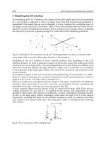
NBT stress-induced threshold voltage shifts. As shown in Fig. 4, experimental lifetime is
obtained as the stress time required that ΔV
T
reaches the predetermined value of FC
(100 mV in this case). Experimental lifetime values, t
i
(i = 1 – 4), are extracted from the plots
shown in the figure and are used to plot the lifetime vs. gate voltage dependence as in the
inset graph, which is further used for extrapolation to a normal operating voltage.
A proper choice of failure criterion, which will be discussed in more details later, is very
important. For example, it can be seen in Fig. 4 that, if the value of FC was higher then about
120 mV, we could not get experimental lifetime for devices stressed with - 30 V at 125°C as
in this case ΔV
T
did not reach 120 mV even after 2000 hours of stressing. Thus, duration of
Implications of Negative Bias Temperature Instability in Power MOS Transistors
325
0.1 1 10 100 1000
0.01
0.1
10 20 30 40 50 60 70
10
2
10
3
10
4
10
5
10
6
10
7
10
8
t3
t4
t2
t1
Lifetime (s)
-V
G
(V)
125
o
C
10 year
t4
t3
t1
V
G
(V)
T=125
o
C
ΔV
T
(V)
Stress time (hours)
-30
-35
-40
-45
t2
FC
ΔV
T
=100mV
Fig. 4. Extraction of experimental lifetime data and illustration of extrapolation to a normal
operating voltage (inset).
the experiment in this case was not sufficient to achieve ΔV
T
as high as FC, which means the
stress time should have been extended to exceed the device lifetime for a given combination
of stress bias and temperature. However, this could require the stressing to be done beyond
the reasonable time limit so in such cases it is convenient to use an adequate fitting model
capable to provide reliable prediction of ΔV
T
on the basis of available data. The simplest
way is to use regular exponential model (Liu et al., 2001; Liu et al., 2002; Krishnan &
Kol’dyaev, 2002):
)]/exp(1[)(
max
τ
tVtV
TT
−
−
Δ
=
Δ
, (6)
where ΔV
Tmax
is the saturation level of threshold voltage shift and
τ
is the characteristic time
constant. However, as shown in Fig. 5, this model (dotted line) in our case yields very poor
agreement with experimental data and significantly underestimates ΔV
T
in saturation. Since
the ΔV
T
time dependences in our devices exhibit the discontinuities manifested as three
distinct stress phases (Figs. 2 and 3), better agreement with experimental data is expected
from the modified version of the above model, which is known as the 2-tau exponential
model and is given by (Liu et al., 2001; Liu et al., 2002):
)]/exp(1[)]/exp(1[)(
2211
τ
τ
tVtVtV
T
−
−
Δ
+
−
−
Δ
=
Δ
, (7)
where the fitting parameters τ
1
and τ
2
represent the time constants closely related to
transitions from early to the second stress phase and from the second phase to saturation,
respectively, whereas ΔV
1
and ΔV
2
are associated with corresponding V
T
shifts. This model
is suitable for processes which have two distinct mechanisms operating one after the other
with 100τ
1
< τ
2
. As can be seen in Fig. 5, the 2-tau model (dashed line) yields fairly good
agreement with experimental data. However, this model appears very sensitive to small
fluctuations in experimental data (the fit looks “wavy” in the second stress phase) and tends
to exaggerate saturation in the case of devices stressed with - 30 V at 125°C, which does not
seem justified by the experimental data.
Micro Electronic and Mechanical Systems
326
0.1 1 10 100 1000
10
-3
10
-2
10
-1
10
0
stretched exponential model
2-tau exponential model
exponential model
ΔV
T
=150 mV
ΔV
T
=100 mV
experimental
fitting
T(
o
C)
ΔV
T
(V)
Stress time (hours)
-45 175
-30 125
V
G
(V)
Fig. 5. Fitting of the NBT stress-induced V
T
shifts by means of various models. Symbols
denote the measurement data and lines are the fits.
Trying to resolve the problem, we have also considered the so-called stretched exponential
model, given by (Van de Walle, 1996; Zafar et al., 2003; Zafar et al., 2004):
)])/(exp(1[)(
max
β
τ
oTT
tVtV −−Δ=Δ
, (8)
where ΔV
Tmax
,
τ
o
, and
β
are the fitting parameters. The stretched exponential model predicts
ΔV
T
would saturate and reach the maximum value only after a very prolonged stressing, so
the ΔV
Tmax
can be taken as a measure of ΔV
T
at ten year device lifetime. Parameter
β
is
defined as a measure of distribution width, and
τ
o
represents a characteristic time constant
of the distribution. This model is suited for processes that, either have two or more distinct
mechanisms each with its own
τ
, or have a single mechanism with statistically distributed
values of
τ
(Van de Walle, 1996).
As can be seen in Fig. 5, the stretched exponential model (solid line) yields very poor
agreement with our experimental data in the early phase of stressing, especially for the
lower stress voltage. However, this disagreement tends to decrease with increase in stress
voltage and/or temperature and, more importantly, the model is in excellent agreement
with experimental data in the second stress phase and in saturation, which is of greatest
practical importance since we need reliable prediction for ΔV
T
at prolonged stress time to
estimate the device lifetime. A practical consequence is that stretched exponential fit, if
properly constructed, may replace the experimental data in saturation and shorten the
experiment execution time, while also allowing the use of higher FC, e.g. 150 mV, as shown
in Fig. 5. Figure also shows that time points associated with transitions from the early to
second stress phase, which had been determined on the basis of parameter n in the t
n
power
law dependences, correspond to the points at which the stretched exponential fitting curves
start agreeing with experimental data, which confirms the phase feature of NBT stress-
induced degradation in power VDMOSFETs (Stojadinović et al., 2005; Danković et al., 2006).
The values of parameter
β
in the stretched exponential fit of our experimental results
obtained on VDMOSFETs are found to vary in the range 0.35∼0.39 independently on stress
Implications of Negative Bias Temperature Instability in Power MOS Transistors
327
conditions, whereas
τ
o
decreases with increasing the stress voltage and temperature, which
all is in good agreement with findings reported in (Zafar et al., 2003; Zafar et al., 2004). The
calculated values of maximum threshold voltage shifts in saturation, ΔV
Tmax
, are listed in
Table 1. As expected, these values, which represent a measure of ΔV
T
at ten year lifetime, are
found to increase with both NBT stress voltage and temperature.
V
G
(V)
ΔV
Tmax
(V)
- 30 - 35 - 40 - 45
125 0.1858 0.2518 0.3109 0.4169
150 0.2073 0.3241 0.4074 0.5563
T (°C)
175 0.3188 0.3319 0.4584 0.5694
Table 1. Values of ΔV
Tmax
in the stretched exponential fit of data obtained on NBT stressed p-
channel power VDMOSFETs
3.2 Extrapolation to normal operating bias conditions
The extracted values of the lifetime under experimental conditions are used as the input
data for extrapolation to normal operating gate bias conditions. However, the results
obtained in this way, which represent the device lifetime values projected to normal
conditions, may be strongly affected by several factors, such as the failure criterion, the
range of gate voltages applied during the stress, and the mathematical function (i.e. model)
used in extrapolation (Aono et al., 2005; Ershov et al., 2005), which are now to be addressed.
3.2.1 Failure criterion
As indicated in Fig. 5, we have defined two different failure criteria as the threshold voltage
shifts of 100 mV and 150 mV, respectively, which are now used to project the device lifetime
under normal gate bias conditions. Lifetime estimation at three different temperatures for
both failure criteria, done by a standard linear extrapolation assuming a maximum normal
operating gate voltage to be V
G
= - 20 V, is illustrated in Fig. 6, whereas the resulting values
of extrapolated lifetime are listed in Table 2. It is quite obvious that lifetime projection
strongly depends on the choice of failure criterion.
The saturation tendency of the stress-induced threshold voltage shift gives contribution to a
rise of the device lifetime, especially for higher failure criterion (150 mV). It can be seen in
Fig. 5 that, in the case of the lower stress voltage, the 150 mV FC line only intersects with the
stretched exponential fitting curve but not with experimental data, which means the
duration of experiment was shorter than the lifetime at given temperature. However, lower
stress voltages are closer to actual operating voltages and are expected to provide more
realistic lifetime projection. In this case, the fact that stretched exponential fit successfully
predicts threshold voltage shift in saturation enabled us to estimate the lifetime by using the
results obtained by fitting instead of the missing experimental ones. If the failure criterion
was too high (e.g. 700 mV), its value would fall far above both experimental and fitting
curves in Fig. 5, which would result into device lifetime tending infinity. Alternatively, too
low failure criterion (below 30 mV) could lead to rather significant underestimation of
device lifetime as the value of failure criterion would fall in the early phase of stressing.
Micro Electronic and Mechanical Systems
328
Following the above considerations, it appears that most reliable lifetime projections can be
obtained by choosing the FC value within the range of threshold voltage shifts observed in
the second and saturation phases of device stressing. The correct choice of FC could be
verified by considering the values of ten year operation voltage, V
G10Y
, which is defined as
the maximum gate voltage that allows ten years of device operation with V
T
shift below the
given FC. As can be seen in Table 3, which shows the V
G10Y
data taken from Fig. 6, the
values of ten year operation voltage in most cases fall below the assumed value of
maximum operating gate bias voltage of - 20 V, except in the case of 150 mV FC at 125°C.
Alternatively, table indicates that in the case of 100 mV FC the devices at 175°C cannot
10 20 30 40 50 60 70
10
0
10
1
10
2
10
3
10
4
10
5
10
6
10
7
10
8
10
9
10
10
10 year
Lifetime (s)
-V
G
(V)
125
o
C
150
o
C
175
o
C
ΔV
T
=100mV
(a)
10 20 30 40 50 60 70
10
0
10
1
10
2
10
3
10
4
10
5
10
6
10
7
10
8
10
9
10
10
ΔV
T
=150mV
Lifetime (s)
-V
G
(V)
125
o
C
150
o
C
175
o
C
10 year
(b)
Fig. 6. Linear extrapolation of the device lifetime at different temperatures for two different
values of failure criteria: a) ΔV
T
=100 mV; b) ΔV
T
=150 mV.
Implications of Negative Bias Temperature Instability in Power MOS Transistors
329
Lifetime (days) ΔV
T
= 100 mV ΔV
T
= 150 mV
125°C
391.07 5792.10
150°C
30.67 289.86
175°C
9.25 48.06
Table 2. Lifetime projections for operating voltage V
G
= - 20 V under two different FC values
approach ten years of operation even without any gate bias, which does not make sense.
Thus, the realistic failure criterion for the devices and experimental conditions used in our
study appears to fall in the 100 - 150 mV range, which yields the ten year operation voltage
within the range of normal gate operation voltages between 0 and - 20 V.
V
G10Y
(V) ΔV
T
= 100 mV ΔV
T
= 150 mV
125°C
-13 -21
150°C
-3 -12
175°C
-5
Table 3. Estimated values of ten year operation voltage under two different failure criteria
3.2.2 Stress voltage range
Another factor that may affect the value of lifetime estimate is the range of stress voltages
used in data extrapolation (Aono et al., 2005). The effects of stress voltage range on
uncertainties of both lifetime projection and ten year operation voltage in the case of
VDMOS devices stressed at 150°C are illustrated in Fig. 7, where the solid line shows
extrapolation over the full range of four different stress voltages applied, whereas the dotted
and dashed lines represent extrapolation over the higher and lower voltage ranges,
respectively (in these cases the data corresponding to the lowest and highest voltages,
respectively, have not been used in extrapolation). As can be noticed in the figure, the
uncertainties associated with the choice of stress voltage range may cause the lifetime
projection to vary for almost one order of magnitude, while the ten year operation voltage,
i.e. maximum allowed V
G
, varies for about 8 V.
A schematic drawing shown in Fig. 8 provides further evidence that the lifetime obtained by
extrapolating the experimental data to normal operating conditions may strongly depend on
the choice of both stress voltage range and failure criterion. As can be seen, experimental
lifetime values determined for a given FC in the cases of devices stressed with the highest
and lowest voltages fall in the early and in saturation phases, respectively. As a result, both
these experimental values are higher, for Δt
2
and Δt
1
, respectively, than those the lifetime
would assume if found in the second phase, leading to a deviation from linearity in the
extrapolation plot shown as an inset graph in Fig. 8. As a consequence, the use of higher
stress voltage range for extrapolation to normal bias conditions tends to underestimate the
lifetime, whereas the use of lower stress voltage range appears to overestimate it, both
contributing to uncertainties shown in Fig. 7. More realistic lifetime estimates could be
Micro Electronic and Mechanical Systems
330
expected if the lower stress voltage range, closer to normal operating voltage, was used in
extrapolation, but in that case the experiment could take too much time, so the most
appropriate solution is to use an expression, such as the one given by stretched exponential
function, that provides good fit to experimental data in the low stress voltage range.
10 20 30 40 50 60 70
10
0
10
1
10
2
10
3
10
4
10
5
10
6
10
7
10
8
10
9
10
10
~1 order of magnitude
E
xtrapolation
uncertainty
of V
G
lower V
G
range
higher V
G
range
Experiment
150
o
C
ΔV
T
=150mV
Lifetime (s)
-V
G
(V)
full V
G
range
uncertainty
of lifetime
10 year
~8 V
Fig. 7. Uncertainties of the lifetime and ten year operation voltage due to different ranges of
stress voltages used in data extrapolation.
Fig. 8. Schematic illustration to explain the effects of FC and stress voltage range on lifetime
projection.
3.2.3 Extrapolation models
In the above analyses of the failure criterion and stress voltage range effects on the lifetime
projection we have only applied the standard model, which was based on linear
extrapolation function. However, it can be seen in Figs. 6 and 7 that this model in some cases
may not provide good fit to experimental data. For this reason, there are several other