Micro Electronic and Mechanical Systems 2009 Part 12 pot
Bạn đang xem bản rút gọn của tài liệu. Xem và tải ngay bản đầy đủ của tài liệu tại đây (1.2 MB, 35 trang )
Micro Electronic and Mechanical Systems
376
4. Modelling the D/A interface
For modelling of the D/A interface, the output circuit of the digital part is to be represented
by a circuit that is supposed to drive an analog load. Note that mixed-mode simulation is
considered. This means that an event scheduler is active, marking the controlling input of
the digital circuit (Litovski & Zwolinski, 1997b). The event scheduler does not allow for two
inputs to be active simultaneously because that is considered as a hazard. Hence, modelling
the output of an inverter is general enough for verification of the modelling procedure.
I
G
0
V
t
I
t
0
t
rf
t
ru
I
0
I
1
a)
b)
Fig. 12. a) Simple D/A conversion circuit, b) Current generator waveform t
ru
stands for the
rising edge while t
rf
for the falling edge duration of the transition
Modelling of the D/A interface is more complex problem than modelling of the A/D
interface, because we need to generate voltage waveform that excites the analog part of the
circuit out of a set of logic states. Conversion algorithms are mostly based on synthesis of an
electronic circuit that replaces the logic element’s output, and is connected as an excitation
to the particular node. Logic gate’s delays also need to be considered and extracted by the
event scheduler.
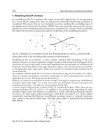
The simplest solution of the D/A conversion is illustrated in Fig. 12. (Zwolinski et al., 1989).
There is a branch consisting of a constant conductance G
0
and current generator I, and it is
applied to D/A node. The delay time is denoted by t
0
.
Ratios I
1
/G
0
and I
0
/G
0
correspond to levels of logic 1 and logic 0, respectively, and different
transition times from logic 1 to 0 and vice-versa, are permitted. Current waveforms for
transitions from logic 1 to 0 and vice-versa are given in Fig. 12b.
A more complex output circuit is shown in Fig. 13. (Arnout & De Man, 1978). There are two
voltage generators (E
0
, R
0
) and (E
1
, R
1
) applied to the analog node depending on logic
element’s output state. This function is realized by a switch controlled by Boolean function.
R
0
and R
1
are logic gate’s output resistances, when there are logic 0 or 1 at the output,
respectively, meaning that there are two different resistance values, in contrast to previous
case, when G
0
was used in both cases. The logic gate’s delay is included in the switching
time instant.
V
R
0
S
0
S
1
R
1
E
0
E
1
+
+
+
Fig. 13. D/A conversion with voltage levels
ANN Application to Modelling of the D/A and A/D Interface for Mixed-mode Behavioural Simulation
377
To further improve accuracy one may use the meliorated version depicted in Fig. 14. (Acuna
et al., 1990). Sequence of pairs (E
i
, R
i
) and voltage controlled switch are used.
V
R
0
S
0
S
1
R
1
E
0
E
1
+
+
+
S
n
R
n
E
n
+
Fig. 14. Conversion when using several signal states on the logic gate output
V
+
C
1
C
0
R
0
E
0
Logic 1
level
Logic 0
level
R
1
E
1
Fig. 15. D/A conversion using pair of voltage controlled resistors
In the circuit in Fig. 15. (Corman & Wimborow, 1988), the logic gate’s output is observed as
a voltage divider output. The capacitance values are constant and determined by the user if
needed, and resistances are nonlinear and determined by user. In the circuits depicted in
Figs. 14. and 15., the logic signal is firstly converted into electrical one and then values of
this analog signal are discretized by comparing to sequence of thresholds. On that basis
switches (Fig. 14.) or resistors values (Fig. 15.) are controlled. The circuits in previous
examples approximate analog signal by discontinuous functions, what is inappropriate for
most nonlinear circuit analysis methods.
Example of an output circuit approximated by analytical function is given in (Petković &
Litovski, 1989; Petković & Litovski, 1991). Only nonlinear resistance is included, and using
an approximation procedure, analytical expressions were produced expressing the output
resistance dependence on the output voltage. Fig. 16. represents the output resistance of a
CMOS inverter as a function of the output voltage. The dashed line is an approximation that
was expressed in closed form.
The circuit depicted in Fig. 17. (Petković & Stojanović, 1992) includes output capacitances
also. It consists of a nonlinear controlled ideal voltage generator E, a nonlinear resistor R
and two output nonlinear capacitors C
0
and C
1
. The transfer function, delays, output
resistance and capacitances of digital gates are precisely modelled. While in (Petković &
Litovski, 1989; Petković & Litovski, 1991) two constant values representing the logic level
were used only, here the transfer characteristics and the delay are expressed in a more
sophisticated way. Namely, a ramp signal, obtained by conversion of the logic output signal
(similarly to Fig. 12b), is first delayed and as such, it represents a controlling signal for the
Micro Electronic and Mechanical Systems
378
nonlinear generator E, whose dependence on the controlling voltage is actually the static
transfer characteristic of an equivalent inverter. C
0
and C
1
are space-charge capacitances of
the complementary transistors in the equivalent inverter.
0.40 1.20 2.00 2.80 3.60 4.40 5.2
0
V
out
(V)
R
out
(k )Ω
2
0
6
0
1
0
0
1
4
0
1
8
0
Fig. 16. Output resistance approximation
Lo
g
ic 1
level
Logic 0
level
V
+
E
+
C
1
C
0
R(E)
E
0
E
1
Fig. 17. D/A conversion using nonlinear reactive part
Analog
voltage
V
DD
V
U
V
SS
v
a
Cv
()
a
V
L
Rs,t
Lr
()
Rs,t
Ur
()
Logic gate’s
output value
s
Fig. 18. Output impedance model
ANN Application to Modelling of the D/A and A/D Interface for Mixed-mode Behavioural Simulation
379
Time-dependent resistors are used in (Nichols et al., 1992). The model of the output
impedance of a logic gate is shown in Fig. 18. The values of the resistances R
U
and R
L
depend on value s, as well as on transition time t
r
, but not on the analog output voltage v
a
.
On the other side the capacitance C depends on this voltage. The voltages V
DD
and V
SS
are
logic gate supply voltages. V
U
and V
L
are fixed offset values for the given type of logic gate.
The resistances R
U
and R
L
linearly change their values from minimum to maximum and
reversely, depending on time t
r
. Linear change does not cause problems in analog
simulation, because the analog voltage value is continuous. The parameter t
r
is chosen large
enough in order to hinder too fast analog voltage change, even if the capacitance value
reaches zero. The capacitance change is given in (Nichols et al., 1992).
Similar solution where resistors change their values is given in (Brown et al., 1994).
In the next, solution based on artificial neural networks is given. Main property of this
solution is its topological generality. Namely, we have no need to look for the topology of
the model depending on the approximation procedure or on the topology of the digital
original. Simply, the topology is always the same. In addition, the approximating function is
general in the sense that only the parameters within the approximating function are
mapping the properties of the instantiated digital circuit.
The topology of the new model is depicted in Fig. 19. In the figure, v
in
stands for a con-
trolling ramp-shaped voltage-waveform:
[
]
)tanh(1)(
max Tinin
vvIvi
−
−
=
, (1)
and Z is a recurrent time-delay neural network approximating the function:
)(iZv
=
out
. (2)
Z
vv
++
in out
++
iv
()
in
v
in
Z
iv
()
in
v
out
Fig. 19. Circuit representation of the model expressed by (1) and (2)
Here, I
max
is the maximum supply current during the transition in the inverter, and v
T
is
(usually) equal to V
DD
/2, V
DD
being the supply voltage. Obviously, the ANN model of Z has
one input (current) and one output (voltage) terminal. The network is trained using input-
output pairs [i(t), v
out
(t)], where i(t) is calculated from (1) while v
out
(t) is obtained by
simulation using the Alecsis simulator of the circuit to be modelled (here an inverter). Note
that we need the electrical schematic of the digital part during the modelling phase.
First results are shown in Fig. 20. Here the output waveforms of the original inverter and the
model are shown to illustrate the quality of the approximation procedure. Unloaded circuits
are simulated. The ANN has five input units (their role being the same as in Table 1.), three
hidden units, and one output unit. Weights and thresholds are given in Table 2.
Micro Electronic and Mechanical Systems
380
No.
Hidden-layer neurons
(First figure stands for
the input neuron)
Output neuron
(First figure stands for
the hidden neuron)
1
w
1
(1,1) = 2.28185
w
1
(2,1) = –3.51137
w
1
(3,1) = 1.36815
w
1
(4,1) = 3.54312
w
1
(5,1) = –1.37367
θ
1
1
= –1.3177
w
2
(1,1) = 0.644039
w
2
(2,1) = 0.644042
w
2
(3,1) = 0.644043
θ
1
2
= –0.408248
2
w
1
(1,2) = 2.28187
w
1
(2,2) = –3.51135
w
1
(3,2) = 1.36816
w
1
(4,2) = 3.54312
w
1
(5,2) = –1.37366
θ
2
1
= –1.31769
3
w
1
(1,3) = 2.28187
w
1
(2,3) = –3.51135
w
1
(3,3) = 1.36816
w
1
(4,3) = 3.54313
w
1
(5,3) = –1.37366
θ
3
1
= –1.31769
Table 2. Weights and thresholds of ANN used to model the inverter circuit.
time [ns]
[V]
v
out
0123456
-1
0
1
2
3
4
5
6
1)
2)
0 1 2 3 4 5 6
time [ns]
6
5
4
3
2
1
0
-1
v
out
[V]
Fig. 20. Responses: 1) of unloaded CMOS inverter (considered as digital output) and 2) of
the new model.
5. Further examples
The following three examples are intended to check the modelling procedure based on
situations not present during training. The first trace (marked 1)) in Fig. 21. is the output
voltage of an inverter being loaded by an inverter, all modelled by regular transistor models,
i.e., obtained by regular circuit simulation. The second one (marked 2)) represents the
ANN Application to Modelling of the D/A and A/D Interface for Mixed-mode Behavioural Simulation
381
response of the same circuit with the ANN model used for the driving part and circuit
model for the loading. This situation was not encountered in the training process. Excellent
agreement was obtained, especially in the steepest part of the response that defines both the
gain and the delay of the loaded inverter.
Further, Fig. 22. gives a similar comparison the loading element here being a transmission
line modelled by a π-RC network (Chatzigeorgiou et al., 2001). Finally, a TTL load (diode)
was used to demonstrate the success of the ANN model in the case of a ‘large’ non-linear
dynamic load, Fig 23. Note the average value of the output voltage is less than 0.5 V while
the difference is still smaller than 10 mV. Once again, the ANN model was developed using
an unloaded inverter.
time [ns]
[V]
v
out
0123456
0
1
2
3
4
5
6
1)
2)
3)
0 1 2 3 4 5 6
time [ns]
6
5
4
3
2
1
0
-1
v
out
[V]
Fig. 21. Responses of 1) inverter loaded by inverter, 2) a model loaded by inverter, and 3) an
ANN (modelling the output) loaded by an ANN modelling the input of an inverter.
time [ns]
[V]
v
out
0123456
0
1
2
3
4
5
6
1)
6
5
4
3
2
1
0
-1
v
out
[V]
0 1 2 3 4 5 6
time [ns]
Fig. 22. Responses of 1) an inverter loaded by RC π -network and 2) a model loaded by RC
π -network.
6. Application to high level analog simulation
Mixed-level analog behavioural modelling may need application of both concepts. In some
situations, one will need to model the output circuit of the driver but in other cases, one will
need to model the input circuit of the load; at very high levels of presentation, one will need
Micro Electronic and Mechanical Systems
382
both. Such an example for the D/A interface is given in Fig. 21. Here trace 3) represents a
response obtained by behavioural simulation using ANN models for both the driver and the
load. In this way, the type of modelling we propose offers the opportunity to be
implemented in analog behavioural simulation at any level.
time [ns]
[V]
v
out
Fig. 23. Responses of a) inverter loaded by a diode and b) ANN model loaded by a diode.
7. Conclusion
An approach to the modelling of the A/D and D/A interface in mixed-mode circuit using
ANNs has been described. The main difference in these two is the type of the input signal
used for capturing the dynamic properties of the circuit to be modelled. For the D/A
interface we use a ramp being, simply, the natural signal, while a sinusoidal signal was used
for the input impedance modelling at the A/D interface in conjunction with general two-
terminal non-linear dynamic modelling.
To summarise, a new method for modelling non-linear dynamic electronic circuits is
described and applied to the modelling of A/D and D/A interfaces for mixed-signal
simulation. It is general and robust. From the point of view of speed of simulation, one should
bear in mind that ANNs are complex structures with exponential non-linearities requiring
additional evaluation time compared to linear models. However, having in mind the
complexity of modern models of MOS transistors (the BSIM3v3 model that is used in most
modern electronic simulation capabilities needs more than a hundred parameters); we claim
that the ANN approach is both efficient and convenient.
8. References
Acuna, E. L., Dervenis, J. P., Pagones, A. J., Yang, F. L., Saleh, R. A. (1990). Simulation
techniques for mixed analog/digital circuits, IEEE Journal of Solid-State Circuits, Vol.
25, No. 2, pp. 353-363, ISSN 0018-9200.
Arnout, G., De Man, H. J. (1978). The use of threshold functions and Boolean-controlled
network elements for macromodelling of LSI circuits, IEEE Journal of Solid-State
Circuits, Vol. SC-13, No. 3, pp. 326-332, ISSN 0018-9200.
ANN Application to Modelling of the D/A and A/D Interface for Mixed-mode Behavioural Simulation
383
Bernieri, A., D'Apuzzo, M., Sansone, L. and Savastano, M. (1994). A Neural Network
Approach for Identification and Fault Diagnosis on Dynamic Systems, IEEE Trans.
on Instrumentation and Measurements, Vol. 43, pp. 867-873, ISSN 0018-9456.
Brown, A. D., Nichols, K. G., Zwolinski, M. and Kazmierski, T. J. (1994). CLASS Simulator
Comparable Mixed-Mode Interfacing, 1994 Research Journal, Department of ECS,
University of Southampton, pp. 99-101, England.
Chatzigeorgiou, A., Nikolaidis, S. and Tsukalas, I. (1999). A Modelling Technique for CMOS
Gates, IEEE Transactions on Computer-Aided Design of Integrated Circuits and Systems,
Vol. 18, pp. 557-575, ISSN 0278-0070.
Chatzigeorgiou, A., Nikolaidis, S. and Tsukalas, I. (2001). Modelling CMOS Gates Driving
RC Interconnect Loads, IEEE Transactions on Circuits and Systems–II: Analog and
Digital Signal Processing, Vol. 48, pp. 413-418, ISSN 1057-7130.
Chow, T. S. W., and Li, X D. (2000). Modelling of Continuous Time Dynamical Systems
with Input by recurrent Neural Networks, IEEE Transactions on CAS–I: Fundamental
Theory and Applications, Vol. 47, pp. 575-578, ISSN 1057-7122.
Citterio, C., Pelagotti, A., Piuri, V. and Rocca, L. (1999). Function Approximation – A Fast-
Convergence Neural Approach Based on Spectral Analysis, IEEE Transactions on
Neural Networks, Vol. 10, pp. 725-740, ISSN 1045-9227.
Corman, T., Wimborow, M. U. (1988). Coupling a digital logic simulator and an analog
circuit simulator, VLSI System Design, pp. 40-47.
Ilić, T., Zarković, K., Litovski, V. B., and Mrčarica, Ž. (2000). ANN Application in Modelling
of Dynamic Linear Circuits, Proceedings of the Small Systems Simulation Symposium,
SSSS'2000, pp. 43-47, Niš, Yugoslavia, September 2000.
Kundert, K. S. (1999). Introduction to RF Simulation and Its Application. IEEE Journal of
Solid-State Circuits, Vol. 34, pp. 1298-1318, ISSN 0018-9200.
Litovski, V. B., Radjenović, J., Mrčarica, Ž. and Milenković, S. (1992). MOS Transistor Model-
ling Using Neural Network, Electronics Letters, Vol. 28, pp. 1766-1768.
Litovski, V. B., Mrčarica, Ž., and Ilić, T. (1997a). Simulation of Non-linear Magnetic Circuits
Modelled Using Artificial Neural Network, Simulation Practice and Theory, Vol. 4,
pp. 553-570, ISSN 0928-4869.
Litovski, V., and Zwolinski, M. (1997b). VLSI Circuit Simulation and Optimization, Chapman
and Hall, ISBN 0412638606.
Litovski, V., Maksimović, D., and Mrčarica, Ž. (2001). Mixed-Signal Modelling With AleC++:
Specific Features of the HDL, Simulation Practice and Theory, Vol. 8, pp. 433-449,
ISSN 0928-4869.
Litovski, V., Andrejević, M. (2002). ANN application in Modelling of A/D interfaces for
mixed-mode behavioural simulation, Proceedings of XLVI Conference of ETRAN, pp.
I51-I54, Banja Vru
ćica, Bosnia & Herzegovina, June 2002.
Litovski, V., Andrejević, M., Damper, R. (2003). Modelling the D/A Interface for Mixed-
Mode Behavioural Simulation, Proceedings of EUROCON 2003, pp. A.130-A.133,
September 2003, Ljubljana, Slovenia.
Litovski, V., Andrejević, M., Petković, P., Damper, R. (2004). ANN Application to Modelling
of the D/A and A/D Interface for Mixed-Mode Behavioural Simulation, Journal of
Circuits, Systems and Computers, Vol. 13, No. 1, pp. 181-192, ISSN 0218-1266.
McAndrew, C. C. (1998). Practical Modelling for Circuit Simulation, IEEE Journal of Solid
State Circuits, Vol. 33, pp. 439-448, ISSN 0018-9200.
Micro Electronic and Mechanical Systems
384
Nichols, K. G., Brown, A. D., Zwolinski, M., and Kazmierski, T. J. (1992). A Logic-Analog
Interface Model, 1992 Research Journal, Department of ECS, University of Southampton,
pp. 106-109, England.
Petković, P., and Litovski, V. (1989). Time Domain Black-box Modelling of CMOS Structures
and Analog Timing Simulation, Proceedings of the Third Annual European Computer
Conference, COMPEURO'89, pp. 5.142-5.143, Hamburg, Germany.
Petković, P., and Litovski, V. (1991). Output Resistance of CMOS Logic Cells, Proceedings of
the 3rd Mid-European Conference on Custom/ASICS, CCC1991, pp. 237-244, Sopron,
Hungary.
Petković, P., Stojanović, Z. (1992). Primena analognih makromodela logičkih ćelija u
modeliranju D/A sprege kod hibridnog simulatora, Proceedings of XXXVI Yugoslav
Conference of ETAN, pp. 51-57, Kopaonik, Yugoslavia.
Trihy, R., and Kundert, K. (1995). Top Down Design with VHDL-A, Proceedings EURO-
SIM’95-Session Software Tools and Products, pp. 53-56, ISBN 0444822410, Vienna,
Austria, September 1995, IEEE Computer Society Press.
Zografski, Z. (1991). A Novel Machine Learning Algorithm and its Use in Modelling and
Simulation of Dynamical Systems, Proceedings of Fifth Annual European Computer
Conference, COMPEURO'91, pp. 860-864, Bologna, Italy.
Zwolinski, M. et al. (1989). The “HOMICIDES“ mixed-mode circuit simulator, Proceedings of
the Silicon Design Conference, Heathrow, England.
22
Electronic Circuits Diagnosis
using Artificial Neural Networks
Miona Andrejević Stošović and Vančo Litovski
University of Niš, Faculty of Electronic Engineering
Serbia
1. Introduction
Whenever we think about why something does not behave as it should, we are starting the
process of diagnosis. Diagnosis is therefore a common activity in our everyday lives
(Benjamins & Jansweijer, 1990). Every complex system is liable to faults or failures. In the
most general terms, a fault is every change in a system that prevents it from operating in the
proper manner. We define diagnosis as the task of identifying the cause and location of a
fault manifested by some observed behaviour. This is often considered to be a two-stage
process: first the fact that fault has occurred must be recognized – this is referred to as fault
detection. That is, in general, achieved by testing. Secondly, the nature and location should be
determined such that appropriate remedial action may be initiated.
The explosion of integrated circuit technology has brought with it some difficult testing
problems. The recent growth of mixed analogue and digital circuits complicates the testing
problem even further. It becomes more complicated to determine a set of input test signals
and output measurements that will provide a high degree of fault coverage. There is also a
timing problem of testing the circuits even on the fastest automated equipment.
The general structure of a diagnostic system is shown in Fig. 1. Signals u(t) and y(t) are input
and output to the system, respectively. Faults and disturbances (here measurement errors)
also influence the system under test, here denoted as the “Process”, but there is no
information about the values of these errors. The task of the diagnostic system is to generate
a diagnostic statement S, which contains information about fault modes that can explain the
behaviour of the Process. Note that the diagnostic system is assumed to be passive i.e. it
cannot affect the Process itself.
The whole diagnostic system can be divided into smaller parts referred here to as tests.
These tests are also diagnostic systems, DS
i
. It is assumed that each of them generates
diagnostic statement S
i
. The purpose of the decision logic (voting system) is then to combine
this information in order to form the final diagnostic statement S.
The number of possible faults in an electronic system may be large and can be located
everywhere in the system. To diagnose in such conditions one frequently uses hierarchical
approach where successive diagnostic statements are generated as the level of description of
the system is lowered going down towards the fault itself (Ho et al., 2001; Sheu & Chang,
1997). This allows for smaller sets of faults to be considered at a time for the given hierarchical
level. Modern automatic test pattern generator may support such concepts (Soma et al., 2001).
Micro Electronic and Mechanical Systems
386
2. Concepts of diagnosis
Besides the human expert that is performing the diagnosis, one needs tools that will help,
and ideally, perform the diagnosis automatically. Such tools are a great challenge to design
engineers because, usually, the diagnostic problem is underspecified. In addition, it is a
deductive process with one set of data creating, in general, unlimited number of hypotheses
among which we try to find a solution. This is why the research community continues to be
attracted by this problem (Bandler & Salama, 1985).
During the life-cycle of a product, testing is implemented in both the production phase and
the implementation phase. We claim, however, that the sustainability of a product is
strongly influenced by the design phase. So, to make a sustainable product, one should
design the test procedure and synthesize test signals early in the design phase.
It is frequently possible to perform functional verification of the system. That, most
frequently, happens when a small number of input/output terminals is present. In the
majority of cases however, full functional testing becomes time consuming and is not
acceptable. So, one applies defect-oriented (structural) testing, as will be discussed in more
detail in what follows.
We consider testing to be: the selection of a set of defects regarded as the most probable, the
description of a set of measurements, the selection of a set of testing points (or output
signals) and most importantly, the synthesis of optimal testing signals that will be applied at
the system inputs allowing for detectability and observability of the listed fault effects. Here,
optimality means that one test signal covers as many faults as possible.
Selection of the type of measurements and testing points is specific to the circuit. One
should stick to those measurements that are prescribed for functional verification. Specific
measurements such as supply current monitoring are frequently adopted, too. Separate test
points may be added in order to improve detectability or observability. Specific design for
testability concepts can be applied.
Thanks to the advances in computational intelligence in the last decades new diagnostic
paradigms have been applied based on: model-based concepts (Benjamins & Jansweijer,
1990); production rule based artificial intelligence (Pipitone et al., 1991); ANNs (Hayashi et
al., 2002); genetic algorithms (Golonek & Rutkowski, 2002); and fuzzy-reasoning (Pous, et
al., 2002); all trying to create an approach that contains properties that we might consider to
be “intelligent behaviour”.
In order to get an idea of why and how ANNs are applied to analogue electronic circuit
diagnosis, the diagnostic concept (Fig. 1) will be elaborated in some detail first. It involves
collaboration of design, test, and field engineers and the mutual distribution of
responsibilities throughout the life cycle of an electronic product. We assume that field
engineers are expected to react after a functional failure of the system. In order to diagnose
such a system they need to be supplied with: testing equipment, a list of specific
measurements to be done (including a set of signals and test points), and diagnostic
software to process the measurement data. A similar set of data and tools would be given to
a test engineer in a production-plant environment in order to evaluate the production yield
and create feedback to process engineers when prototyping the circuit. We believe,
however, design engineers are the most familiar with the product and the most qualified
and capable to synthesize test and diagnostic signals, and procedures. This means the SBT
(simulation before test) has to be applied to create fault dictionaries containing exhaustive
lists of faults and corresponding responses. The fault dictionary is in fact a table
Electronic Circuits Diagnosis using Artificial Neural Networks
387
Fault
s
Disturbances
Process
Voting
system
Diagnostic
statement
S
DS
DS
S
S
DS
S
1
2
2
1
n
n
ut
()
yt
()
Fig. 1. A general diagnostic system.
representing the mapping from the fault list into a list of faulty (or possibly, fault-free)
responses. In that way the diagnostic process becomes a search through the fault dictionary.
Alternatively, modern diagnostic techniques using traditional artificial intelligence and
reasoning methods typically fall into the simulation after test (SAT) category. This will
increase the time spent on diagnosing systems at production time (Spina & Upadhyaya,
1997). SBT systems typically require more initial computational costs, but provide faster
diagnosis at production time being the second reason why this concept was accepted here.
We claim here that ANNs, being universal approximators (Scarselli & Tsoi, 1997), are the
best way both to capture the mapping, and to search through the dictionary, thereby to
perform diagnosis.
3. Diagnosis of nonlinear dynamic analogue circuits
Analogue electronic circuits are known to be difficult to test and diagnose. Apart from the
huge number of possible faults, this difficulty is a consequence of the inherent nonlinearity
of these circuits. Even linear circuits (having linear input-output signal interdependence)
exhibit nonlinear relations between circuit parameters and the output response. There are no
linear active networks. Active networks are nonlinear with nonlinear reactive elements.
They may be linearized and thought of as such in situations where signal and parameter
changes are small in comparison to nominal values. When large parameter changes or even
catastrophic faults occur (affecting the DC state), however, one must distinguish between
linear and analogue circuits. This is not the case in most research reports bringing confusion
into the subject.
Several concepts were applied to diagnosis of analogue networks. Among them we will first
mention the ones relying on reasoning based on measured data and some measure of
distance between the response of the good circuit and the faulty one. Starting with the basic
research reported in (Bandler & Salama, 1985) and (Milor & Visvanathan, 1989) several ideas
were reported. In (Luchetta et al., 2002) the fault location phase is considered as an
optimization problem where the parameter value is searched for in order to minimize the
difference among the actual and simulated response. Linear circuits in the frequency
domain are considered being characterized by symbolic functions. Similarly, in (Catelani &
Micro Electronic and Mechanical Systems
388
Giraldi, 1998) applying SAT multiple faults may be diagnosed in linear circuits described by
symbolic functions what is characterized as model based method. SBT based method for soft
faults diagnosis in linear circuit was proposed in (Alippi et al., 2002) where harmonic
analysis was used for selecting the most suitable test input stimuli and nodes by means of
global sensitivity approach. In (Huang & Cheng, 2000) and (Yoon et al., 1998) passive
circuits were diagnosed based on graph theoretical approach, and on pass and fail regions
for the circuit poles and zeroes in the real-imaginary plane, respectively, while in (Chang,
2002) a Boolean decision scheme was proposed for the diagnosis of linear circuits described
in the frequency domain. In order to diagnose multiple soft faults in the same type of
circuits the Woodbury formula was applied to the modified nodal equation to construct the
so called fault equation in (Liu & Starzyk, 2002). A decomposition method was proposed in
(Starzyk & Liu, 2002) aiming to cope with circuit complexity. In one approach, small
parameter changes were allowed in nonlinear circuits (Tadeusuewicz et al., 2002). Soft faults
were considered only when linear programming method was used for diagnostic decisions.
Large parametric fault diagnosis was described in (Worsman & Wong, 2002) using
piecewise linear models for DC analysis, and separate considerations were given for
diagnosis of faults in the dynamic part of the network (considered linear) based on large
change sensitivity computations. Further, in (Cota et al., 1999) the diagnostic method
applied consists of injecting probable faults in a mathematical model of the linear circuit,
and later comparing its output with the output of the real faulty circuit. Transfer functions
transformed into the Z domain were created and fault injection was performed. In
(Cherubal & Chatterjee, 1999) methodology based on linear regression model using prior
circuit simulation which relates a set of measurements to the circuit's internal parameters
was applied in order to solve for the circuit parameter values using iterative numerical
techniques. Linear circuits in the frequency domain were diagnosed in (El-Yazeed &
Mohsen, 2003) where the AC response to a set of sinusoidal input frequencies was
calculated at selected test nodes. Prony's method was then utilized as a preprocessor to
extract an optimal set of features representing nodal voltage waveforms. In (Dai & Xu, 1999)
a solution to the same problem was proposed based on noise measurements.
Soft and hard faults (shorts and opens) in nonlinear dynamic circuit were diagnosed in
(Pinjala et al., 2003). The procedure employs a statistical method of computing Mahalanobis
distance to find defects in load board traces and components. Short list of defects was
reported. A low-noise amplifier was diagnosed in (Liobe & Margala, 2004) by using digital
signatures suitable for built-in self test design concepts. Hard and soft faults were diagnosed
the former modelled as resistors having convenient values.
A specific aspect of diagnosis is the number and location of the test points. Simply, we can
say that internal test points should be avoided and measurements on the primary inputs
and outputs are preferred. This is not only related to their automatic accessibility but also to
the nature of the diagnostic reasoning. Namely, one looks for functionality to diagnose
something, and the function is seen at the primary terminals. Of course, in order to
compensate for the small number of test points more measurements with different types of
applied signals are, generally, needed to extract complete information about the system
behaviour. For complex analogue systems, however, hierarchical approaches based on
decomposition (Ho et al., 2001; Sheu & Chang, 1997; Bandler & Salama, 1985; Starzyk & Liu,
2002) are inevitable provided that no propagation of the fault effect arises between partitions
what is not easy to achieve. Of course, there are circuits that may be partitioned based on
functionality known a priori from the design process as mentioned in the introduction.
Electronic Circuits Diagnosis using Artificial Neural Networks
389
Another aspect of fundamental importance is related to the choice of the output quantities
that are to be measured. In most cases these are voltages at the output of the circuit under
test (CUT) or at selected test points. It is shown, however, that measurement of the supply
current (Iddq) may be successfully used for testing of both analogue and digital circuit
(Dragic & Margala, 2002; Margala et al., 2002; Papakostas & Hatzopoulos, 1991; Bell et al.,
1991; Zwolinski et al., 1996). This idea was used for diagnosis of analogue circuits using
ANN that will be discussed later.
Several results were reported where the so called artificial intelligence concepts were
applied to diagnosis of analogue circuits or at least linear ones. In (Savioli et al., 2005)
method based on fault trajectory concept for fault diagnosis of analog linear continuous time
networks, which relies on evolutionary techniques, where a genetic algorithm (GA) was
coded to optimize test vector generation, was reported. GA was applied into (Golonek &
Rutkowski, 2002) creation “transfer functions“ enabling creation of a new type of fault
dictionary. The classical signature dictionary has been replaced by fault decoder based on
transfer functions. In order to obtain a sharp diagnosis about the possible wrong component
of the circuit, a tool based on qualitative reasoning was used in (Pous et al., 2002). In
particular, the results were refined by means of fuzzy techniques. This means that inputs,
outputs, rules and the corresponding operators to combine them were defined. A
production rule based concept was reported in (Pipitone et al., 1991).
ANNs have previously been applied to diagnosis (Spina & Upadhyaya, 1997; Materka, 1994;
Rodrigez et al., 1994; Aminian & Aminian, 2000; He et al., 2002; Andrejević & Litovski, 2004;
Aminian et al., 2002; Stopjakova et al., 2004; Yu et al., 1994; Collins et al., 1994; Catelani &
Gori, 1996; Maidon et al., 1997; Yang et al., 2000). As in the case with the classical concepts,
however, ANNs were predominantly applied to linear analogue circuits. In (Materka, 1994)
feed-forward ANNs were used for parameter identification (soft fault diagnosis) of linear
circuits. In (Rodrigez et al., 1994) linear power networks were diagnosed by feed-forward
ANNs. In order to enhance the performance of the ANN applied for diagnosing of soft
faults in linear active networks, in (Spina & Upadhyaya, 1997), new “criteria“ - a
discriminating measure based on discrepancy of the autocorrelation function of the fault-
free and the correlation function of the faulty and fault-free circuit, were introduced. The
same problem was attacked in (Aminian & Aminian, 2000; Aminian et al., 2002) where the
impulse response was analyzed by wavelet decomposition, principal component analysis,
and data normalization preprocessors before introduced to the ANN. Soft faults were
considered only. In (He et al., 2002) a method based on extraction of a “feature vector“ from
the differences between vectors of node voltages of faulty and fault-free linear circuit for
every fault was described. This feature vector is then presented to the ANN as a teaching
session. Network tearing is applied in order to manage the circuit complexity in an 11
transistor bipolar circuit. Every partition was considered linear although catastrophic faults
were present (e.g. transistor base disconnected). Two faults were diagnosed only. In
(Andrejević & Litovski, 2004) a linear resistive circuit was diagnosed using feed-forward
neural nets. Soft and hard faults (shorts and opens) were considered. Comparably large set
of faults was taken into account. In the scheme presented in (Catelani & Gori, 1996) (one
opamp/one capacitor, three resistors and two diodes) programmable function generator
was used to generate the set of stimuli sequentially injected into the input of the CUT. Six
test frequencies were chosen. For each stimulus the frequency response of the CUT has been
considered and five Fourier components were measured at the output test point with the
spectrum analyzer. For the purpose of diagnosis, four neural networks were used. Euclidian
Micro Electronic and Mechanical Systems
390
distance was to be learned by the ANN in order conclusions to be created on the origin of
the fault. Bipolar analogue integrated circuits (Maidon et al., 1997) were diagnosed and their
resistances determined from the magnitudes of the Fourier harmonics in the spectrum
responses to a sinusoidal input test signal using multilayer perceptron ANN. The input
vector to the ANN consists of the magnitudes of the Fourier harmonics of the response
waveforms owing to the input stimulus, and the class represents the type of circuit faults,
while the outputs map to resistance values of the faults. Probabilistic neural network was
applied in (Yang et al., 2000). It is a four layer feedforward neural network that realizes the
Bayes classifier. The ANN creates the probability that a circuit is faulty and points to the
type of fault. In (Stopjakova et al., 2004) a large number of circuit versions was created by
introducing sets of models for every separate fault. In fact, hard faults were considered
while the opens and the shorts were modelled by resistors of variable resistivity. Then
statistical properties of the time domain response (in this case the supply current) to a pulse
excitation were extracted in order to create knowledge of the fault to fault-effect mapping.
The supply current was successfully used for diagnosing gate oxide shorts in CMOS circuits
by the help of ANNs in (Yu et al., 1994; Collins et al., 1994). After introducing a fault model
of the MOS transistor built as a series connection of two MOS transistors with a common
gate (i.e. considering this as a soft fault), several faults per transistor (for all transistors in an
11 transistor operational amplifier) were created by changing the possible position of the
gate short relative to the source-to-drain ends of the channel. Sinusoidal and ramp signals
were used for creation of a fault dictionary in an SAT method. The response i.e. the supply
current was sampled to give a series of values used to train the feed-forward (Yu et al., 1994)
and a Cohonen (Collins et al., 1994) neural network.
In this chapter we will give two examples of fault diagnosis in non-linear dynamic circuit.
The first one refers to an analogue circuit, and the second to the mixed-mode circuit.
We describe the results of applying feed-forward ANNs to the diagnosis of non-linear
dynamic electronic circuits with no restriction on the number and type of faults. This
method is based on fault dictionary creation and using an ANN for data compression by
memorizing the table representing the fault dictionary. Only DC and small signal sinusoidal
excitations will be applied, so preserving the usual measurement procedure for generating
the data given in a component’s and/or a circuit’s data-sheets. The ANN so created is,
consequently, used for diagnosis by applying to it the signals obtained by measuring the
faulty network. This process may be considered as looking-up a fault in the fault dictionary.
The ANN finds the most probable fault code that corresponds to the measured signals.
Putting this in the general context of diagnosis we first note that the fault dictionary
contains all the knowledge we need. In other words by applying the SBT concept all
hypotheses are memorized (within the ANN) and no further hypothesis needs to be created
after the dictionary is known. This is equivalent to the structural concept of testing. The fault
not conceived in advance can't be tested nor diagnosed. Now we look among the
hypotheses (by searching the dictionary i.e. by running the ANN) to find the one most
similar to the actual (faulty) circuit response. The difficulties here are the complexity of the
search and the decision algorithm that finds the “most similar” entry in the dictionary. As
will be shown with an example this can be an extremely difficult task. It has been
successfully solved using ANNs.
The network used for the first diagnostic example is a feed-forward neural network
structured in three layers. It has only one hidden layer, which has been proved sufficient for
Electronic Circuits Diagnosis using Artificial Neural Networks
391
this kind of problem (Masters et al., 1993). The neurons in the hidden layer are activated by
a sigmoidal function, while the neurons in the output layer are activated by a linear
function. The learning algorithm used for training this network is a version of the steepest-
descent minimization algorithm (Zografski et al., 1991).
4. Fault dictionary creation and application example
In order to describe the way in which the fault dictionary was created, the circuit in Fig. 2 is
used as an application example. This is a CMOS operational amplifier consisting of seven
transistors. To our knowledge this example belongs to the category of the most complex
ones reported, both from the number of circuit elements point of view and the number of
faults inserted. Note that three (nonlinear) capacitors are associated with every transistor
totalling the number of nonlinear circuit elements to 28 but, for the sake of simplicity, are
not shown in the figure. In order to emphasize the method as such, while not offering a full
solution of the diagnostic problem for this circuit, having in mind abundance of possible
faults, a reduced set of faults was considered. To this end only single transistor faults are
sought. That, of course will not affect the generality of the ideas implemented in the next.
We do not intend to diagnose simultaneous presence of several faults.
C
R
R
V
V
V
V
R
T
T
TT
T
T
2
o
i+i-
dd
1
1
5
34
6
2
SC7DS
SC7GD
SC7GS
OC7G
OC7S
OC7D
Fig. 2. The operational amplifier circuit. SC=short circuit, OC=open circuit
Ten faults per transistor, six catastrophic and four parametric were added to the dictionary.
As shown in the figure (using T
7
as an example) there exist three open-circuit faults (OC)
and three short-circuit faults (SC) per transistor (for example, OC3G stands for open gate of
transistor T
3
, and SC1DG stands for drain and gate shorted in transistor T
1
, Table 1.). As
opposed to (Stopjakova et al., 2004) and some others, the shorts (some of them behaving as
bridging fault) and opens were really implemented instead of resistors modelling them. To
effectively simulate perfect short and opens we used our model of the ideal switch (Mrčarica
et al., 1999) what is not possible in the SPICE simulator. Of course, there was no obstacle for
us to use resistors to model shorts and opens. Simply, what we did, we considered
satisfactory. In addition, two faulty values for every channel length (±20%) (denoted as L+
and L- in Table 1.), and two for every channel width (±20%) (denoted as W+ and W- in Table
1.) were introduced, totalling 10 faults per transistor. The soft faults considered here are
Micro Electronic and Mechanical Systems
392
expected to model design errors and, in a specific way, gate oxide short having in mind the
fault model reported in (Yu et al., 1994). For the whole circuit this gives a set of 70 faults
observed.
The DC output values (V
oDC m
) were first obtained by simulation. Here m=0,1,2,…,69 stands
for the fault code. In addition, the frequency response of the circuit (the non-inverting input
terminal was excited by a signal of amplitude 1mV) was obtained by simulation over a fixed
frequency range in order to extract two response parameters: the nominal gain (A
m
) and the
3-dB cut-off frequency (f
3dBm
). For the example given, we considered this signature to be
satisfactory complex. If additional fault need to be used one might think on additional
measurements such as supply current. Note that, for the DC supply current point of view,
the fault effects of most open faults at sources and drains in series connected transistors,
may have equivalent signatures.
Type
A
m
f
3dBm
[MHz] V
oDCm
[V]
Code (m)
FF 419 0.01527 0.127 0
1L+ 0.0053 6.791 0.0497 37
OC1G 0.047 501.187 0.127 49
OC3G 0.049 544.042 0.093 47
SC1DG 0.042 320.440 0.0458 6
SC2DS 0.071 312.071 3.3 27
SC5DS 0.656 0.57 0.0186 55
6W- 5770 0.0018 0.2146 13
OC5D 0.056 507.298 3.3 25
SC5GS 0.109 0.036 0 2
Table 1. Part of the fault dictionary for the circuit of Fig. 2. The faults are chosen at random.
Because of the nonlinearity of the circuit, every fault is expected to change the transistor's
quiescent points. Consequently, new linear transistor-models are created by SPICE-like
program and used for frequency domain performance extraction for each fault. In order to
find the new quiescent point for every fault, we have to insert the fault i.e. to create a faulty
model of the circuit for DC analysis. This procedure is described elsewhere (Milovanović &
Litovski, 1991; Milovanović & Litovski, 1994) and will not be discussed here.
Fault SC3DG is untestable because of the existing connection between the gate and drain of
T
3
. This reduces the fault dictionary to 69 elements. Therefore, the fault dictionary created
here has four columns containing the set of circuit performances i.e. the signatures and the
fault code: {V
oDCm
, A
m
, f
3dBm
, m}. First three items in a row are considered inputs to the neural
network, while the fault code is learnt as an output.
The fault coding is an important issue. In fact, some defects exhibit very similar effects. So,
input data (signatures) can have very close numerical values, and if the output values
(defect codes) were also similar, the network could not always be trained successfully. Such
an example is given in Fig. 3. Here the signatures of three faults are compared. By careful
inspection we can see that only the f
3dB
values suggest a difference between the fault effects.
Faults are coded randomly, so that faults with similar effects are unlikely to have similar
codes. This approach is proven to be good, because the way of coding influenced the
training time, and also, the training error. Part of the fault dictionary for the circuit in Fig. 2,
is given in Table 1., where m=0 denotes the fault-free circuit.
Electronic Circuits Diagnosis using Artificial Neural Networks
393
0
0.5
1
1.5
2
2.5
3
3.5
4
d
e
f
e
c
t
4W
-
d
e
f
e
c
t
1W
-
d
e
f
e
c
t
4
L
+
AA A
f
[MH ]
3dB
Z
f
[MH ]
3dB
Z
f
[MH ]
3dB
Z
Vo
[V]
Vo
[V]
Vo
[V]
f
3dB
A
f
3dB
f
3dB
A
A
V
o
V
o
V
o
Fig. 3. Fault effects of faults 4W-, 4L+ and 1W-
Here we come to an additional issue concerning the applicability of rule-based approaches
to the diagnosis of systems of this kind. Because of the similarity of the circuit performance
in the presence of different faults, no set of rules can be established to distinguish between
these three faults. Furthermore, by inspection of Table 1., we can see that the performance
values cover a broad range. For example, for the voltage gain, the smallest value in the Table
is 0.0053, and the largest is 5770. So, we cannot establish a rule defining the difference that
occurs as a consequence of the presence of a certain fault. Thus rule-based approaches are
impractical for systems exhibiting responses as continuous functions. Note, in addition, that
we expect noisy data to be obtained when field measurements are performed for diagnosis
which further complicates the creation of any rules. We may claim that similar is related to
use fuzzyfication in order to boost the difference among signatures. To go further, this puts
in a similar prospective the simulation-after-test i.e. the model based concept. Namely, in
this concept one is supposed to create a set of hypotheses that will be checked against the
measurement data by successive simulations of the circuit under test at the repairing site.
Having in mind Fig. 3., however, we do not believe the creation of a qualified set of
hypotheses is an achievable task.
The fault dictionary can be further reduced in size by processing the ambiguity groups or the
groups of equivalent faults. According to (Manetti & Piccirilli, 2003) “an ambiguity group is,
essentially, a group of components where, in case of fault, it is not possible to uniquely
identify the faulty one”. Here, we can say that an ambiguity group consists of a set of faults
that propagate identical signatures to the output, making the faults detectable and the
circuit testable, but no distinction between the individual faults is possible making them
undiagnosable. Table 2. shows all ten ambiguity groups for this example, systematically
Micro Electronic and Mechanical Systems
394
collected after simulation. The faults italicized in Table 2. represent the same topological
connection in the circuit, so the effect would be expected to be the same.
Ambiguity
group
Faults included A
f
3dB
[MHz] V
oDC
[V]
1
OC1D
0.31 20000 0.0179
OC1S
2
OC3D
0.041 365.8 3.3
OC3S
3
OC4D
0.303 20000 0.0458
OC4S
SC4GS
SC3GS
SC3DS
4
OC5D
0.056 507.298 3.3
OC5S
5
OC6D
0.063 0.039 3.3
OC6S
6
OC7D
∞
→A
Indeterminate 0
OC7S
7
SC1GS
0.055 515.993 3.3
SC2GS
8
SC5GS
0.109 0.036 0
SC7GS
9
SC4DS
A=0 Indeterminate 3.3
SC6GS
SC7DS
10
3L+
0.05 2.37 3.3
4W+
Table 2. Ambiguity groups and fault effects.
A specific ambiguity group is the case when the gain (A) although small ever rises within
the given frequency range. This is denoted as
∞
→A . The 3-dB cut-off frequency is in these
cases indeterminate. Some of defects exhibiting this property, however, have different V
oDC
values, so they can be distinguished. In these cases, to avoid use of infinite numbers during
the training of the ANN we assigned a value of 1000 to the gain. This is the case when
simulating defects OC7S and OC7D, but since these defects produce completely the same
effect, they form ambiguity group number 6.
A similar situation occurs when the gain is almost zero, A=0. The 3-dB cut-off frequency is
then again indeterminate. Ambiguity group number 9 covers three such defects, with the
same V
oDC
.
Only one representative of each ambiguity group was included in the fault dictionary. From
Table 2., we find that the complete fault dictionary in this case has 70-1-24+10=55 elements.
With three pieces of data for each fault, the neural network input structure was restricted to
three input terminals. The ANN diagnoses the fault by outputting the fault-code (m) as a
signal level, so we needed only one output neuron. The number of hidden neurons, n, was
Electronic Circuits Diagnosis using Artificial Neural Networks
395
found by trial and error after several iterations starting with an estimation based on that in
(Baum & Haussler, 1989). The goal was to find the optimum n that leads to a satisfactory
classification even with noisy excitations. Using too many neurons would increase the
training time, but using too few would starve the network of the resources needed to solve
the problem. Also, an excessive number of hidden neurons may cause the overfitting
problem (Masters et al., 1993), when a network has so much information capability that it
learns insignificant aspects of the training sets, irrelevant to the general population. In
practice, 30 hidden neurons were used. After successful training, no mistakes were observed
for all 55 faults.
Code
A
j
f
3dBj
[MHz]
V
oDCj
[V]
ANN
response
0 419
0.0145
0.127 -0.02128
1 129.6
0.0248
0.079 1.09057
2 0.109 0.036
-0.05
2.01405
3 6028
0.001575
0.1712 2.93868
5 4453
0.002415
1.0255 5.03203
6
0.0441
320.44 0.0458 6.03224
9 1000 1000 -0.05 9.0707
10
0.043
365.8 3.3 10.0278
12 1000 1000
3.39
12.1771
13 5770
0.00171
0.2146 13.2376
16 8220
0.00197
0.4876 16.031
18 0.32 1000
0.133
17.8458
20 0 1000
3.46
20.4409
21 0.83 1000
3.46
20.6497
25
0.0588
507.298 3.3 25.0605
26 11.739
0.114
0.127 26.0098
27 0.071 312.071
3.46
27.0091
34 5809
0.00169
0.1811 33.7541
35 209 0.0237
0.115
35.47
36
0.05
1000 0.8824 36.3514
37
0.00556
6.791 0.0497 37.2652
43
0.004
17.191 0.0509 43.0008
46
0.0523
515.993 3.3 45.99
47
0.0514
544.042 0.093 47.0133
49
0.04935
501.19 0.127 49.042
50 6030
0.001425
0.2466 49.9284
52 0.005 133.757
3.46
52.0044
53 119.4
0.0258
0.0843 53.0205
54 0.041
428
3.3 53.5346
55 0.688 0.57 0.0186 54.8614
Table 3. Inputs with noise and ANN responses.
The generalization property of the network was verified by supplying noisy data to its
inputs. This is presented in Table 3. 30 samples were examined. For each sample, one input
Micro Electronic and Mechanical Systems
396
(boldfaced in the Table 3.) is incremented by +5% or -5%, representing noise generated
during the measurement process. The responses of the network are given in the last column
of the table. The ANN response was considered to be correct (i.e. acceptable) when its value
was in the range [(m-0.5), (m+0.5)]. We can see that all faults can still be diagnosed though
some with difficulties (for m=20, 35, and 54).
In the previous text we have presented our first results in the development of a new
technique for fault diagnosis of nonlinear dynamic circuits. The method we proposed may
be summarised as follows.
In applying ANNs to the diagnosis of nonlinear dynamic electronic circuits, as described,
we have demonstrated the implementation of the method and a set of results. These results
vindicate the technique. In further work we intend to resolve the elements of ambiguity
groups. In addition, more complex systems will be considered and larger fault dictionaries
generated. Consequently additional measurements will be needed in order to keep the
number of test points low. This will, hopefully, allow for implementation of these ideas to
diagnosis of mixed-signal circuits.
5. Fault diagnosis in digital part of sigma-delta converter
Further in this text we will show that feed-forward ANN may be applied to the diagnosis of
non-linear dynamic electronic circuits (Andrejević & Litovski, 2006a; Andrejević et al., 2006;
Andrejević, 2006) that are mixed with digital ones. Two types of defects in the digital part of
the circuit will be considered: effects of rising and falling edge delays in logic gates and
catastrophic defects that change the circuit topology. Similar procedure may be applied to
diagnosis in analog part of the circuit (Andrejević & Litovski, 2006b).
The simulation before test concept was adopted. This means that after choosing the set of
faults of interest (say the most probable ones), repetitive simulation is performed in order to
create the system response for every fault. Codes are associated to the responses and used as
part of the fault dictionary that, in addition, contains the faulty responses themselves. Of
course, the responses are represented in a form that is easy to manipulate.
The ANN is first trained for modelling the look-up table. This means that faulty responses
are repeatedly brought to the input, while the ANN is forced to present the fault codes at its
output. Then, the ANN running with the given vector of stimuli (measured output signals
of a faulty or, possibly, fault free system) may be viewed as search of the look-up table. The
ANN response, if the network properly trained, will immediately find the fault and produce
the fault code at its output.
The procedure applied is reminiscent to the one implemented to analog circuits in (Litovski
et al., 2006). To our knowledge this is the first application of ANNs to diagnosis of mixed
signal circuit.
6. Faults in the specific circuit design
As an example of a complex circuit, the sigma-delta modulator in Fig. 4. is chosen (Xu &
Lucas, 1995).
This is a mixed-signal circuit, having both analogue and digital elements. Switches in the
circuit are modelled as truly ideal switches, with zero resistance for closed switch and
infinite resistance for open switch. Simulations are performed using Alecsis (Glozić, 1994)
simulator.
Electronic Circuits Diagnosis using Artificial Neural Networks
397
R
DQ
QC
400ns
400ns
Analog
input
C
RR
R
C
Clk
ϕ
1
ϕ
2
1-bit
Output
ϕ
11
ϕ
12
ϕ
22
ϕ
21
n3
n7
sw1
sw2
V
refp
V
refn
1
34
1
2
2
INV1
INV4
INV2
NA1 NA2 NA3 NA4
INV3
Fig. 4. Sigma-delta modulator architecture.
The integrator charging time is invariable with respect to clock rate in order to keep the gain
constant. This means that the analog switch must be turned on for fixed time duration
regardless of clock rate. This is achieved by using monostable multivibrator as a fixed-width
pulse generator in the circuit.
The monostable multivibrator between the clock input and switch control block functions as
a pulse generator to produce control signals of fixed time duration. Fig. 5 shows reaction of
the system when the input is excited by a ramp signal.
We consider in this chapter defects only in the digital part of the circuit. There are two types
of defects observed: catastrophic defects and delays of rising and falling edge of output
digital signals. These delay defects are neither catastrophic, nor parametric, because there is
no change in circuit topology, and no change in element values.
Digital signal can be “stuck-at-1” or “stuck-at-0”. In the circuit in Fig. 4., analogue switches
are controlled by digital signals, so there are pairs of the same fault effects, such as: the effect
is the same when the switch is stuck at ON (OFF) and the logic circuit's output is “stuck-at-
1” (“stuck-at-0”). So, we will consider hard faults (which refer to the analogue part of the
circuit) as stuck switches (Andrejević et al., 2006). The cases when switches in the feedback
loop (ϕ
11
, ϕ
12
, ϕ
21
, ϕ
22
) are permanently closed are excluded, because voltage references V
refp
and V
refn
would be shorted in such cases.
Having in mind that clock period in the circuit is 1.2μs (half period is 600ns), we examined
effects of delays not greater than 400ns. In fact, effects of rising edge delay are simulated for
values of delay: 100ns, 250ns, 400ns, and for falling edge, we simulated smaller values: 50ns,
100ns, 150ns. The goal was to determine how these delays influence the output, and whether
different delay values produce different outputs (Andrejević et al., 2006). All digital gates are
examined (4 inverters and 4 nand circuits). The first conclusion was that delays in the circuit of
inverter 2 (INV2) do not influence output signal, meaning that output is not changed. Further,
there exist groups of delays causing the same effect. Such groups are known as ambiguity
groups, and they are listed in Table 4. The first four groups show the same effect of delays. In
the second column of the Table 4, defects causing the same effects are named, and accordingly,
third column presents that same effect (signature). The fifth ambiguity group is in a way
different. The members of that group are both catastrophic and delay defects. Note that only
one representative of each group is given in the fault dictionary, Table 5.
Micro Electronic and Mechanical Systems
398
Ambi
g
uit
y
g
roup
D
e
f
ect t
y
pe Si
g
nature
1
na3(tf=50ns)
104108210
na4(tr=250ns)
2
na3(tr=400ns)
102104208
na4(tr=400ns)
3
na4(tf=100ns)
404210240
inv3(tf=100ns)
4
FF
20440480A
inv2(tr=50ns)
inv2(tr=100ns)
inv2(tr=150ns)
inv2(tf=50ns)
inv2(tf=100ns)
inv2(tf=150ns)
5
ϕ21OFF
000000000
na1(tf=150ns)
sw1ON
Table 4. Ambiguity groups.
-1.45
-0.15
1.15
-1.80
0.10
2.00
-1.00
-0.10
0.80
output
input (V)
n3
(V)
n7 (V)
0 50 100 150 200
time (ms)
Fig. 5. Simulation results for ramp excitation
Fault dictionary is created using the response of the circuit to an input ramp signal. The
circuit output value is registered after every clock period, so these output digital values
form the output signature. These are then represented in more compact hexadecimal presen-
tation. Accordingly, fault dictionary is created as shown in Table 5. It must be noted that
defects are coded randomly, while it is very important that defects with similar signatures
must not have similar fault codes. If this happens, it may be very difficult, or even
impossible for ANN to recognize defects. In the second column of Table 5., defects are
coded. First column describes the type of the defect, relative to notation given in Fig. 4.
(inv3(tf=50ns) stands for the falling edge delay in inverter 3 and na1(tr=400ns) for the rising
Electronic Circuits Diagnosis using Artificial Neural Networks
399
edge in nand 1). FF stands for the fault free circuit. The third column contains the signature
seen at the output.
Defect type
D
e
f
ec
t
code
Signature Defect type
D
e
f
ec
t
code
Signature
FF 0 20440480A inv4(tf=100ns) 23 220220821
sw1OFF 1 996999999 sw2ON 24 018018030
inv1(tr=150ns) 2 000010010 inv3(tr=150ns) 25 104208210
na1(tr=400ns) 3 31C352C66 inv4(tr=100ns) 26 050050110
inv1(tf=50ns) 4 811105024 na3(tr=250ns) 27 021041084
na1(tf=100ns) 5 008000010 inv4(tr=150ns) 28 0440900C0
na2(tf=50ns) 6 404811044 na1(tr=100ns) 29 844889112
na3(tr=400ns) 7 102104208 na3(tf=100ns) 30 082202208
na3(tf=50ns) 8 104108210 inv4(tf=50ns) 31 208210420
na3(tf=150ns) 9 030018090 na4(tf=100ns) 32 404210240
na4(tr=100ns) 10 204110210 sw2OFF 33 996696699
ϕ21OFF
11 000000000 inv1(tf=150ns) 34 092430918
inv1(tf=100ns) 12 848504890 na2(tf=150ns) 35 811104844
na2(tr=100ns) 13 102081042 inv1(tr=50ns) 36 040810108
na2(tf=100ns) 14 410842209 inv3(tf=150ns) 37 802408420
inv3(tr=100ns) 15 202404410 inv4(tf=150ns) 38 010840882
na3(tr=100ns) 16 808809021 na2(tr=250ns) 39 080408104
inv1(tr=100ns) 17 004020040 na1(tr=250ns) 40 149463131
na2(tr=400ns) 18 020101008 inv3(tf=50ns) 41 402804411
inv4(tr=50ns) 19 088108210
ϕ12OFF
42 300038003
na1(tf=50ns) 20 100110012
ϕ22OFF
43 925129252
na4(tf=50ns) 21 402804420 inv3(tr=50ns) 44 204208410
ϕ11OFF
22 001C00038 na4(tf=150ns) 45 802408811
Table 5. Fault dictionary.
ANN was trained for modelling the look-up table. It is a feed-forward neural network with
one hidden layer. The signatures are inputs to the network, and the fault code is network
output to be learned. It means that the neural network has 9 inputs (one input per
hexadecimal digit) and one output neuron. Hexadecimal values are presented as decimal
when they are inputs to the network. After learning was completed, the number of hidden
neurons in the resulting ANN was 10, what was found by trial and error after several
iterations starting with an estimation based on (Masters et al., 1993; Baum & Haussler, 1989).
The structure of the obtained ANN is verified by exciting the ANN with faulty inputs. Res-
ponses of the ANN show that there were no errors in identifying the faults what is
presented in Table 6. Only negligible discrepancies may be observed.
7. Conclusion
In applying ANNs to the diagnosis of nonlinear dynamic electronic circuits, as described,
we have demonstrated the implementation of the method and a set of results.
In the second part of this chapter, effects of delay and catastrophic defects in sigma-delta
modulator were examined. The diagnosis was successful.
Micro Electronic and Mechanical Systems
400
Accordingly, we may conclude that ANNs are convenient and powerful means for
diagnosis, and, what is important, realizable as a hardware that may be as fast as necessary
to follow the changes of the system's response in real time.
Defect type
D
e
f
ec
t
code
ANN
output
Defect type
D
e
f
ec
t
code
ANN
output
FF 0 -0.000215 inv4(tf=100ns) 23 22.9998
sw1OFF 1 0.999861 sw2ON 24 23.9997
inv1(tr=150ns) 2 1.99969 inv3(tr=150ns) 25 24.9999
na1(tr=400ns) 3 2.99981 inv4(tr=100ns) 26 26.0009
inv1(tf=50ns) 4 3.99985 na3(tr=250ns) 27 27
na1(tf=100ns) 5 4.99988 inv4(tr=150ns) 28 28
na2(tf=50ns) 6 6.00003 na1(tr=100ns) 29 29.0001
na3(tr=400ns) 7 7.00006 na3(tf=100ns) 30 30
na3(tf=50ns) 8 7.99998 inv4(tf=50ns) 31 31.001
na3(tf=150ns) 9 8.99991 na4(tf=100ns) 32 32.0003
na4(tr=100ns) 10 10.0004 sw2OFF 33 33.0021
ϕ21OFF
11 10.9998 inv1(tf=150ns) 34 34
inv1(tf=100ns) 12 11.9997 na2(tf=150ns) 35 34.9998
na2(tr=100ns) 13 12.9994 inv1(tr=50ns) 36 36
na2(tf=100ns) 14 13.9997 inv3(tf=150ns) 37 37.0001
inv3(tr=100ns) 15 15 inv4(tf=150ns) 38 37.9998
na3(tr=100ns) 16 15.9996 na2(tr=250ns) 39 39.0024
inv1(tr=100ns) 17 16.9998 na1(tr=250ns) 40 40.0015
na2(tr=400ns) 18 18 inv3(tf=50ns) 41 40.9997
inv4(tr=50ns) 19 19.0018
ϕ12OFF
42 41.9996
na1(tf=50ns) 20 19.9997
ϕ22OFF
43 42.9998
na4(tf=50ns) 21 20.9999 inv3(tr=50ns) 44 43.9997
ϕ11OFF
22 22 na4(tf=150ns) 45 44.9996
Table 6. ANN output results.
8. References
Alippi, C., Catelani, M., Mugnaini, M. (2002). SBT Soft Fault Diagnosis in Analog Electronic
Circuits: A Sensitivity-Based Approach by Randomized Algorithms, IEEE
Transactions on Instrumentation and measurement, Vol. 51, No. 5, pp. 1116-1125.
Aminian, M., and Aminian, F. (2000). Neural-network based analog-circuit fault diagnosis
using wavelet transform as preprocessor, IEEE Transactions on CAS – II: Analog and
Digital Signal Processing, Vol. 47, No. 2, February 2000, pp. 151-156.
Aminian, F., Aminiam, M., Collins, H. W. (2002). Analog Fault Diagnosis of Actual Circuits
Using Neural Networks, IEEE Trans. On Instrumentation and Measurement, Vol. 51,
No. 3, June 2002, pp. 544-50, ISSN 0018-9456.
Andrejević, M., Litovski, V. (2004). ANN application in electronic diagnosis-preliminary
results, Proceedings of IEEE 24
th
International Conference on Microelectronics MIEL
2004, pp. 597-600, Niš, Serbia, May 2004.