Optical Fibre, New Developments Part 3 ppt
Bạn đang xem bản rút gọn của tài liệu. Xem và tải ngay bản đầy đủ của tài liệu tại đây (1.99 MB, 35 trang )
OpticalFibre,NewDevelopments64
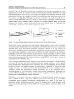
In the experiment, the fiber has been laid across a section of wave flume, which is
essentially a long water channel equipped with a wave generator at one end and a wave
absorbing device at the other end; hence the fiber serves as a point sensor acting as a wave
gauge. The fiber sensor is capable of detecting water wave frequencies accurately for all
types of wave generated by the flume. With the optimum sag of fiber, the output response
of the optical fiber sensor is linear within 0.7 m ± 0.2 m wave level. Fig. 14 is the wave
measurement by the wave gauge and fiber sensor.
The sensor monitors the polarization state change induced intensity variation of the light
when the sensing fiber is affected by the presence of the water wave. As a result, the sensing
fiber should be fully submerged in the water and be able to be moved physically by the
water wave for the frequency range of 1-10 Hz, although the vibration sensor can have a
KHz response signal. The sensor is capable of providing accurate frequency distributions for
both regular waves and irregular waves, confirmed by a conventional wave gauge.
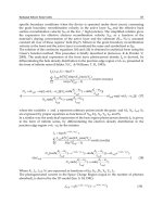
8. Spectral analysis of POTDR for intrusion sensing
Up to now, distributed optical fiber sensors have been mainly studied for static
measurements, i.e. no time-varying or slowly time-varying signals, such as, static strain or
temperature. Dynamic measurements using the above techniques are difficult to achieve
because of the large number of waveforms required to average out the polarization effect
induced signal fluctuation or because of the large range of frequency scans that are needed
in order to obtain a reasonable signal to noise ratio (SNR) and spatial resolution over a
kilometer fiber length.
A frequency modulated source to realize distributed Brillouin sensor based on correlation of
pump and probe in fiber is demonstrated for vibration measurement (Hotate & Ong, 2003].
However, each time only one sensing point is chosen by the correlation peak of pump and
probe light, it is particularly suitable for material processing over a short fiber distance
while it is not essentially a fully distributed sensor which should provide information for
every point along the fiber under test simultaneously. A truly distributed vibration sensor
has been demonstrated recently based on the spectrum density of POTDR system (Zhang &
Bao, 2008b). This new sensor can detect a vibration frequency of 5 KHz over 1 km sensing
length with 10 m spatial resolution.
POTDR was developed as the first fully distributed optical fiber measurement for static
physical parameters in the earlier 80’s (Rogers, 1981) and then adopted as a diagnostic tool
in optical communication systems to identify high polarization mode dispersion (PMD)
fiber sections (Gisin et al., 1999). In conventional POTDR, the SOP is measured with 4
polarization controllers so that the rotation angle of SOP can be measured in every location
to recover the PMD or strain, this process takes minutes, as a result, it can only be used for
static measurement. To realize dynamic measurement with ms time scale, only one polarizer
is sufficient to identify dynamic events, through which the birefringence change along the
fiber could be detected; the setup is shown in Fig. 15. Moreover, with a novel fast Fourier
transform (FFT) spectrum analysis, multiple simultaneous events with different vibration
frequencies or even with the same frequencies are able to be accurately located. The spectral
density function of location change is equivalent to many variable narrowband filters with
bandwidth of < 1Hz to improve the SNR of multiple events detection, which allows the
disturbance to be detected simultaneously at any location along the sensing fiber.
Fig. 15. Experimental setup of POTDR system
Data processing for the POTDR is done using four steps: in step (1) a large number of
POTDR curves are acquired, step (2) at a particular position the time domain plot can be
acquired from multiple POTDR curves, step (3) the FFT can be performed at that position
using the time domain information and step (4) by performing steps (2) and (3) at all points
along the fiber the magnitude of a certain frequency can be plotted as a function of distance.
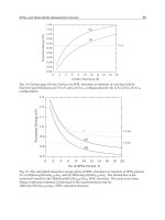
The post-signal processing is shown in Fig. 16. Step (1) to (3), is employed here by taking an
average every 100 POTDR curves in step (2). Considering a 10 kHz repetition rate of the
pulsed light, the effective sampling rate becomes 100 Hz, which has set the limitation for
impact wave detection. Fig. 17(a) plots the FFT spectrum of 1.5 seconds time domain data at
550 m with a peak at 22 Hz when the PZT is driven by 5 Vpp, 22 Hz square wave. Benefited
to its high sensitivity, this POTDR system makes it possible to measure higher frequency
disturbance without any averaging in step (2). Hence, the maximum detectable frequency is
5 kHz using a 10 kHz sampling rate. In Fig. 17(b) when the driven frequency of the piezo is
set to 4234 Hz, this peak frequency is clearly shown in the FFT spectrum at 550 m.
Fig. 16. The data processing of the spectrum density of POTDR
FiberSensorApplicationsinDynamicMonitoringofStructures,
BoundaryIntrusion,SubmarineandOpticalGroundWireFibers 65
In the experiment, the fiber has been laid across a section of wave flume, which is
essentially a long water channel equipped with a wave generator at one end and a wave
absorbing device at the other end; hence the fiber serves as a point sensor acting as a wave
gauge. The fiber sensor is capable of detecting water wave frequencies accurately for all
types of wave generated by the flume. With the optimum sag of fiber, the output response
of the optical fiber sensor is linear within 0.7 m ± 0.2 m wave level. Fig. 14 is the wave
measurement by the wave gauge and fiber sensor.
The sensor monitors the polarization state change induced intensity variation of the light
when the sensing fiber is affected by the presence of the water wave. As a result, the sensing
fiber should be fully submerged in the water and be able to be moved physically by the
water wave for the frequency range of 1-10 Hz, although the vibration sensor can have a
KHz response signal. The sensor is capable of providing accurate frequency distributions for
both regular waves and irregular waves, confirmed by a conventional wave gauge.
8. Spectral analysis of POTDR for intrusion sensing
Up to now, distributed optical fiber sensors have been mainly studied for static
measurements, i.e. no time-varying or slowly time-varying signals, such as, static strain or
temperature. Dynamic measurements using the above techniques are difficult to achieve
because of the large number of waveforms required to average out the polarization effect
induced signal fluctuation or because of the large range of frequency scans that are needed
in order to obtain a reasonable signal to noise ratio (SNR) and spatial resolution over a
kilometer fiber length.
A frequency modulated source to realize distributed Brillouin sensor based on correlation of
pump and probe in fiber is demonstrated for vibration measurement (Hotate & Ong, 2003].
However, each time only one sensing point is chosen by the correlation peak of pump and
probe light, it is particularly suitable for material processing over a short fiber distance
while it is not essentially a fully distributed sensor which should provide information for
every point along the fiber under test simultaneously. A truly distributed vibration sensor
has been demonstrated recently based on the spectrum density of POTDR system (Zhang &
Bao, 2008b). This new sensor can detect a vibration frequency of 5 KHz over 1 km sensing
length with 10 m spatial resolution.
POTDR was developed as the first fully distributed optical fiber measurement for static
physical parameters in the earlier 80’s (Rogers, 1981) and then adopted as a diagnostic tool
in optical communication systems to identify high polarization mode dispersion (PMD)
fiber sections (Gisin et al., 1999). In conventional POTDR, the SOP is measured with 4
polarization controllers so that the rotation angle of SOP can be measured in every location
to recover the PMD or strain, this process takes minutes, as a result, it can only be used for
static measurement. To realize dynamic measurement with ms time scale, only one polarizer
is sufficient to identify dynamic events, through which the birefringence change along the
fiber could be detected; the setup is shown in Fig. 15. Moreover, with a novel fast Fourier
transform (FFT) spectrum analysis, multiple simultaneous events with different vibration
frequencies or even with the same frequencies are able to be accurately located. The spectral
density function of location change is equivalent to many variable narrowband filters with
bandwidth of < 1Hz to improve the SNR of multiple events detection, which allows the
disturbance to be detected simultaneously at any location along the sensing fiber.
Fig. 15. Experimental setup of POTDR system
Data processing for the POTDR is done using four steps: in step (1) a large number of
POTDR curves are acquired, step (2) at a particular position the time domain plot can be
acquired from multiple POTDR curves, step (3) the FFT can be performed at that position
using the time domain information and step (4) by performing steps (2) and (3) at all points
along the fiber the magnitude of a certain frequency can be plotted as a function of distance.
The post-signal processing is shown in Fig. 16. Step (1) to (3), is employed here by taking an
average every 100 POTDR curves in step (2). Considering a 10 kHz repetition rate of the
pulsed light, the effective sampling rate becomes 100 Hz, which has set the limitation for
impact wave detection. Fig. 17(a) plots the FFT spectrum of 1.5 seconds time domain data at
550 m with a peak at 22 Hz when the PZT is driven by 5 Vpp, 22 Hz square wave. Benefited
to its high sensitivity, this POTDR system makes it possible to measure higher frequency
disturbance without any averaging in step (2). Hence, the maximum detectable frequency is
5 kHz using a 10 kHz sampling rate. In Fig. 17(b) when the driven frequency of the piezo is
set to 4234 Hz, this peak frequency is clearly shown in the FFT spectrum at 550 m.
Fig. 16. The data processing of the spectrum density of POTDR
OpticalFibre,NewDevelopments66
Fig. 17. Piezo fiber stretcher driven by 5 Vpp square wave, FFT spectrum of time trace signal
at 550 m of (a) 22 Hz driven signal; (b) 4234 Hz driven signal
The present sensing uses post-signal processing, with the introduction of a micro-processor
there would be a significant reduction of the signal processing time without going through
computer for digitization and programming timing, which makes the current system
response in the ms time frame, as the FFT signal processing and averaging can be conducted
by electronic circuits directly. This new technology could in a cost-effective manner provide
intrusion sensing for perimeter security at various places or structure health monitoring for
large structures, such as bridges, highway pavements, pipeline leakage, etc. with low fault
rate due to the multiple frequency components discrimination at < 1 Hz narrow band.
9. Conclusion
Monitoring of health is not a new idea and it is literally practiced by physicians using a
knowledge base, tools, methods, and systems for diagnosis and then prognosis of one’s state
of health. Some of these tools were specifically developed for the practice of medicine and in
a similar fashion this occurred in the current chapters.
The ability to accurately and efficiently monitor the long-term performance of engineering
structures is an extremely valuable one. The potential benefits of structural monitoring
includes reducing lifetime maintenance costs, improved safety and the ability to confidently
use more efficient designs and advanced materials.
Today, a new and interdisciplinary area of structural health monitoring is likewise needed
in order to address the structural, economic, and safety needs of the 21st century society and
beyond. As with other industries, civil engineering must also undergo such a catharsis for a
similar industry development.
In this Chapter we focused on fiber sensors using birefringence properties which have the
fastest response to dynamic changes, using this idea combined with nonlinear effects we
have demonstrated point and distributed sensors for dynamic monitoring in structures,
communication fibers and security applications.
10. References
Allen, C.; Kondamuri, P.; Richards, D. & Hague, D. (2003). Measured temporal and spectral
PMD characteristics and their implications for network-level mitigation
approaches.
J. Lightwave Technol., Vol. 21, No. 1, (January 2003) 79–86,
doi:10.1109/JLT.2003.808634
Bao, X.; W. Li, W.; Zhang, C.; Eisa, M.; El-Gamal S. & Benmokrane, B. (2008). Monitoring the
distributed impact wave on concrete slab due to the traffics based on polarization
dependence on the stimulated Brillouin scattering.
Smart Mater. Structures, Vol. 17,
No. 1, (November 2008) 1-5, doi:10.1016/j.engstruct.2004.05.018
Barnoski, J. K. & Jensen, S. M. (1976). Fiber waveguides: A novel technique for investigation
attenuation characteristics.
Appl. Opt., Vol. 15, No. 9, (Sept. 1976) 2112-2115
Boyd, R. W. (2003).
Nonlinear Optics, Second Edition, Academic Press, ISBN: 0-12-121682-9,
San Diego
Brosseau, C. (1998).
Fundamentals of Polarized Light: A Statistical Optical Approach, Wiley Inter-
Science, ISBN: 978-0-471-14302-4, New York
Cameron, J.; Chen, L.; Bao, X. & Stears, J. (1998). Time evolution of polarization mode
dispersion in optical fibers.
Photon. Technol. Lett., Vol. 10, No. 9, (September 1998)
1265–1267, ISSN: 1041-1135
Chen, L.; Zhang, Z. & Bao, X. (2007). Combined PMD-PDL effects on BERs in simplified
optical systems: an analytical approach.
Opt. Express, Vol. 15, No. 5, (March 2007)
2106-2119, doi:10.1364/OE.15.002106
Gisin, N.; Gisin, B.; der Weid, J. P. V. & Passy, R. (1996). How accurately can one measure a
Statistical Quantity like Polarization-Mode Dispersion?.
Photon. Technol. Lett., Vol.
8, No. 12, (December 1996) 1671–1673, ISSN: 1041-1135
Gordon, J. P. & Kogelnik, H. (2000). PMD fundamentals: polarization mode dispersion in
optical fibers.
Proc. Nat. Acad. Sci., Vol. 97, No. 9, (April 2000) 4541-4550, PMID:
10781059
Hotate, K. & Ong, S. L. (2003). Distributed dynamic strain measurement using a correlation-
based Brillouin sensing system.
IEEE Photon. Technol. Lett., Vol. 15, No. 2, (February
2003) 272–274, ISSN: 1041-1135
Hunttner, B.; Gisin, B. & Gisin, N. (1999). Distributed PMD measurement with a
polarization-OTDR in optical fibers
. J. Lightwave Technol. Vol. 17, No. 10, (October
1999) 1843-1848, ISSN: 0733-8724
Huttner, B.; Geiser, C. & Gisin, N. (2000). Polarization-induced distortion in optical fiber
networks with polarization-mode dispersion and polarization-dependent losses.
IEEE J. Select. Topics Quantum Electron., Vol. 6, No. 2, (March/April 2000) 317-329,
ISSN: 1077-260X
Karlsson, M.; Brentel, J. & Andrekson, P. (2000). Long-term measurement of PMD and
polarization drift in installed fibers.
J. Lightw. Technol., Vol. 18, No. 7, (July 2000)
941–951, ISSN: 0733-8724
Krispin, H.; Fuchs, S. & Hagedorn, P. (2007). Optimization of the efficiency of aeolian
vibration dampers,
Proceeding of Power Engineering Society Conference and Exposition
in Africa
, South Africa, pp 1-3, ISBN: 978-1-4244-1477-2, July 2007, IEEE
PowerAfrica '07, Johanesburg
FiberSensorApplicationsinDynamicMonitoringofStructures,
BoundaryIntrusion,SubmarineandOpticalGroundWireFibers 67
Fig. 17. Piezo fiber stretcher driven by 5 Vpp square wave, FFT spectrum of time trace signal
at 550 m of (a) 22 Hz driven signal; (b) 4234 Hz driven signal
The present sensing uses post-signal processing, with the introduction of a micro-processor
there would be a significant reduction of the signal processing time without going through
computer for digitization and programming timing, which makes the current system
response in the ms time frame, as the FFT signal processing and averaging can be conducted
by electronic circuits directly. This new technology could in a cost-effective manner provide
intrusion sensing for perimeter security at various places or structure health monitoring for
large structures, such as bridges, highway pavements, pipeline leakage, etc. with low fault
rate due to the multiple frequency components discrimination at < 1 Hz narrow band.
9. Conclusion
Monitoring of health is not a new idea and it is literally practiced by physicians using a
knowledge base, tools, methods, and systems for diagnosis and then prognosis of one’s state
of health. Some of these tools were specifically developed for the practice of medicine and in
a similar fashion this occurred in the current chapters.
The ability to accurately and efficiently monitor the long-term performance of engineering
structures is an extremely valuable one. The potential benefits of structural monitoring
includes reducing lifetime maintenance costs, improved safety and the ability to confidently
use more efficient designs and advanced materials.
Today, a new and interdisciplinary area of structural health monitoring is likewise needed
in order to address the structural, economic, and safety needs of the 21st century society and
beyond. As with other industries, civil engineering must also undergo such a catharsis for a
similar industry development.
In this Chapter we focused on fiber sensors using birefringence properties which have the
fastest response to dynamic changes, using this idea combined with nonlinear effects we
have demonstrated point and distributed sensors for dynamic monitoring in structures,
communication fibers and security applications.
10. References
Allen, C.; Kondamuri, P.; Richards, D. & Hague, D. (2003). Measured temporal and spectral
PMD characteristics and their implications for network-level mitigation
approaches.
J. Lightwave Technol., Vol. 21, No. 1, (January 2003) 79–86,
doi:10.1109/JLT.2003.808634
Bao, X.; W. Li, W.; Zhang, C.; Eisa, M.; El-Gamal S. & Benmokrane, B. (2008). Monitoring the
distributed impact wave on concrete slab due to the traffics based on polarization
dependence on the stimulated Brillouin scattering.
Smart Mater. Structures, Vol. 17,
No. 1, (November 2008) 1-5, doi:10.1016/j.engstruct.2004.05.018
Barnoski, J. K. & Jensen, S. M. (1976). Fiber waveguides: A novel technique for investigation
attenuation characteristics.
Appl. Opt., Vol. 15, No. 9, (Sept. 1976) 2112-2115
Boyd, R. W. (2003).
Nonlinear Optics, Second Edition, Academic Press, ISBN: 0-12-121682-9,
San Diego
Brosseau, C. (1998).
Fundamentals of Polarized Light: A Statistical Optical Approach, Wiley Inter-
Science, ISBN: 978-0-471-14302-4, New York
Cameron, J.; Chen, L.; Bao, X. & Stears, J. (1998). Time evolution of polarization mode
dispersion in optical fibers.
Photon. Technol. Lett., Vol. 10, No. 9, (September 1998)
1265–1267, ISSN: 1041-1135
Chen, L.; Zhang, Z. & Bao, X. (2007). Combined PMD-PDL effects on BERs in simplified
optical systems: an analytical approach.
Opt. Express, Vol. 15, No. 5, (March 2007)
2106-2119, doi:10.1364/OE.15.002106
Gisin, N.; Gisin, B.; der Weid, J. P. V. & Passy, R. (1996). How accurately can one measure a
Statistical Quantity like Polarization-Mode Dispersion?.
Photon. Technol. Lett., Vol.
8, No. 12, (December 1996) 1671–1673, ISSN: 1041-1135
Gordon, J. P. & Kogelnik, H. (2000). PMD fundamentals: polarization mode dispersion in
optical fibers.
Proc. Nat. Acad. Sci., Vol. 97, No. 9, (April 2000) 4541-4550, PMID:
10781059
Hotate, K. & Ong, S. L. (2003). Distributed dynamic strain measurement using a correlation-
based Brillouin sensing system.
IEEE Photon. Technol. Lett., Vol. 15, No. 2, (February
2003) 272–274, ISSN: 1041-1135
Hunttner, B.; Gisin, B. & Gisin, N. (1999). Distributed PMD measurement with a
polarization-OTDR in optical fibers
. J. Lightwave Technol. Vol. 17, No. 10, (October
1999) 1843-1848, ISSN: 0733-8724
Huttner, B.; Geiser, C. & Gisin, N. (2000). Polarization-induced distortion in optical fiber
networks with polarization-mode dispersion and polarization-dependent losses.
IEEE J. Select. Topics Quantum Electron., Vol. 6, No. 2, (March/April 2000) 317-329,
ISSN: 1077-260X
Karlsson, M.; Brentel, J. & Andrekson, P. (2000). Long-term measurement of PMD and
polarization drift in installed fibers.
J. Lightw. Technol., Vol. 18, No. 7, (July 2000)
941–951, ISSN: 0733-8724
Krispin, H.; Fuchs, S. & Hagedorn, P. (2007). Optimization of the efficiency of aeolian
vibration dampers,
Proceeding of Power Engineering Society Conference and Exposition
in Africa
, South Africa, pp 1-3, ISBN: 978-1-4244-1477-2, July 2007, IEEE
PowerAfrica '07, Johanesburg
OpticalFibre,NewDevelopments68
Landau, L. & Lifchitz, E. M. (1981).
Electrodynamics of Continuous Media (J. B. Sykes & J. S.
Bell, Trans.), Pergamon Press, ISBN: 0080091059, Oxford (Original work published
1969)
Leeson, J; Bao X.; Côté, A. (2009). Polarization Dynamics in Optical Ground Wire (OPGW)
Network.
Appl. Opt., Vol. 48, No. 14, (May 2009) 2214-2219,
doi:10.1364/AO.48.002214
Measures, R. M. (2001).
Structural Monitoring with Fibre Optics Technology, Academic Press,
ISBN: 0-12-487430-4, London
Rogers, A. J. (1981). Polarization-optical time domain reflectometry: A technique for the
measurement of field distributions.
Appl. Opt., Vol. 20, No. 6, (March 1981) 1060-
1074, ISSN: 0003-6935
Snoody, J. (2008).
Study on Brillouin Scattering in Optical Fibers with Emphasis on Sensing.
Unpublished master's thesis, University of Ottawa, Ottawa, Canada
Waddy, D.; Lu, P.; Chen, L. & Bao, X. (2001). Fast state of polarization changes in aerial fiber
under different climatic conditions.
Photon. Technol. Lett., Vol. 13, No. 9, (September
2001) 1035–1037, ISSN: 1041-1135
Waddy, D. S.; Chen, L. & Bao, X. (2005). Polarization effects in aerial fibers
. Opt. Fiber
Technol., Vol. 11, No. 1, (October 2005) 1-19, doi:10.1016/j.yofte.2004.07.002
Wuttke, J.; Krummrich, P. & Rosch, J. (2003). Polarization oscillations in aerial fiber caused
by wind and power-line current.
Photon. Technol. Lett., Vol. 15, No. 6, (June 2003)
882–884, ISSN: 1041-1135
Zhang, Z.; Bao, X.; Yu, Q. & Chen, L. (2006). Fast states of polarization and PMD drift in
submarine fibres.
Photon. Technol. Lett., Vol. 18, No. 9, (May 2006) 1034-1036, ISSN:
1041-1135
Zhang, Z.; Bao, X.; Yu, Q. & Chen, L. (2007). Time evolution of PMD due to the tides and sun
radiation on submarine fibers.
Opt. Fiber Technol., Vol. 13, No. 1, (January 2007) 62-
66, doi:10.1016/j.yofte.2006.07.003
Zhang, Z & Bao, X. (2008a). Continuous and damped vibration detection based on fiber
diversity detection sensor by rayleigh backscattering.
J. Lightwave Technol., Vol. 26,
No. 7, (April 2008) 852-838, ISSN: 0733-8724
Zhang, Z. & Bao, X. (2008b). Distributed optical fiber vibration sensor based on spectrum
analysis of polarization-OTDR system.
Opt. Express, Vol. 16, No. 14, (July 2008)
10240-10247, doi:10.1364/OE.16.010240
Zhang, Z.; LeBlanc, S.; Bao X. (2008a). Concrete pavement vibration monitoring due to the
car passing using optical fiber sensor,
Proceedings of the 19th International Conference
on Optical Fibre Sensors (OFS-19)
, pp.1-5, ISBN: 9780819472045, Australia, June 2008,
SPIE, Perth
Zhang Z.; Bao X.; Rennie C. D.; Nistor I. & Cornett A. (2008b). Water wave frequency
detection by optical fiber sensor.
Opt. Communication, Vol. 281, No. 24, (December
2008) 6011–6015, ISSN: 0030-4018
Near-FieldOpto-ChemicalSensors 69
Near-FieldOpto-ChemicalSensors
AntoniettaBuosciolo,MarcoConsales,MarcoPisco,MicheleGiordanoandAndreaCusano
X
Near-Field Opto-Chemical Sensors
Antonietta Buosciolo
1
, Marco Consales
2
, Marco Pisco
2
,
Michele Giordano
1
and Andrea Cusano
2
1
National Research Council,
Institute for Composite and Biomedical Materials
Napoli, Italy
2
University of Sannio,
Optoelectronic Division, Engineering Department,
Benevento, Italy
1. Introduction
Nanotechnology and nanoscale materials are a new and exciting field of research. The
inherently small size and unusual optical, magnetic, catalytic, and mechanical properties of
nanoparticles not found in bulk materials permit the development of novel devices and
applications previously unavailable. One of the earliest applications of nanotechnology that
has been realized is the development of improved chemical and biological sensors.
Remarkable progress has been made in the last years in the development of optical
nanosensors and their utilization in life science applications.
This new technology demonstrates the breadth of analytical science and the impact that will
be made in the coming years by implementing novel sensing principles as well as new
measurement techniques where currently none are available.
What is exciting in sensor research and development today? This is a tough question. There
are many significant innovations and inventions being made daily. Micro and
nanotechnology, novel materials and smaller, smarter and more effective systems will play
an important role in the future of sensors.
With the increasing interest in and practical use of nanotechnology, the application of
nanosensors to different types of molecular measurements is expanding rapidly. Further
development of delivery techniques and new sensing strategies to enable quantification of
an increased number of analytes are required to facilitate the desired uptake of nanosensor
technology by researchers in the biological and life sciences.
To fulfil the promise of ubiquitous sensor systems providing situational awareness at low
cost, there must be a demonstrated benefit that is only gained through further
miniaturization. For example, new nanowire-based materials that have unique sensing
properties can provide higher sensitivity, greater selectivity and possibly improved stability
at a lower cost and such improvements are necessary to the sensor future.
Nano-sensors can improve the world through diagnostics in medical applications; they can
lead to improved health, safety and security for people; and improved environmental
monitoring. The seed technologies are now being developed for a long-term vision that
5
OpticalFibre,NewDevelopments70
includes intelligent systems that are self-monitoring, self-correcting and repairing, and self-
modifying or morphing not unlike sentient beings.
On this line of argument, in last years, our interdisciplinary group has been involved in
research activities focused on the development of novel opto-chemical nano-sensors
employing near-field effects to enhance the overall performance of the final device.
In this chapter, thus, we report recent findings on new class of opto-chemical sensors whose
excellent sensing performance are related to an enhancement effect of the optical near-field
induced by semiconductive structures of tin dioxide (SnO
2
) when their spatial dimensions
are comparable to the employed radiation wavelength ().
The main objective is to investigate the possibility to concentrate the electro-magnetic field
in precise localized spots, by means of metal oxide micro and nano-sized structures, to
increase light matter interaction and provide innovative and valuable sensing mechanisms
for next generation of fiber optic chemical and biological nano-sized sensors (Pisco et al.,
2006; Buosciolo et al., 2006).
Due to the strong interdisciplinary nature of the problem, research activities have been
carried out following an integrated approach where all the aspects (material selection,
integration techniques and transducer development), have been simultaneously addressed
and optimized.
Taking this line, interest was focused on issues like investigation of the surface morphology
and of the near-field optical properties in relation to suitable processing and post-processing
conditions; correlation of the surface layer morphology and the emerging near-field
intensity distribution with the sensing performance [Consales et al., 2006b; Cusano et al.,
2006). We found that sensitive layers with very rough morphologies inducing a significant
perturbation of the optical near-field, exhibited surprisingly sensing performance for both
water chemicals monitoring and against chemical pollutants in air environment, at room
temperature (Cusano et al., 2006; Buosciolo et al., 2008b).
Similar effects of light manipulation have been observed, in recent years, only in noble metal
nanostructures explained in terms of localized surface plasmons and in subwavelength hole
arrays in both metal films and non metallic systems; in a recent convincing theoretical
model (Lezec & Thio, 2004) relative to the last case, the transmission of light is modulated
not by coupling to surface plasmons, but by interference of diffracted evanescent waves
generated by subwavelength periodic features at the surface, leading to transmission
enhancement as well as suppression.
In light of this argument, it is clear that the manipulation of light through semicondutive
micro and nano sized structures opens new frontiers not only in sensing applications but
have also vast potential to be applied in many fields ranging from high performance
nanometer-scale photonic devices up to in-fiber micro systems.
Here, we review the technological steps carried out by our group for the demonstration of a
novel sensing mechanism arising from near-field effects in confined domains constituted by
particle layers of tin dioxide with size approaching the optical wavelength. To this aim, we
have structured the present chapter as follows: sections 2 and 3 are focused on the
properties and characteristics of tin dioxide as sensing layer for chemical transducers with
particular emphasis on the state of the art on chemical sensors based on this type of
semiconductor. Section 4 deals with the principle of operation of the proposed reflectometric
opto-chemical sensors and with the electrostatic-spray pyrolysis method as valuable tool to
deposit particle layers of tin dioxide on optical fiber substrates at wavelength scale. Section 5
reports the morphological and optical characterization of the so produced superstrates
carried out by atomic force and scanning near-field optical microscopy, very useful to
clearly outline the effects of processing parameters on particles size and distribution as wells
on the optical near-field emerging from the overlays. Finally, in section 6 we present the
sensing performances of fiber optic chemo-sensors incorporating tin dioxide particle layers
in both air and liquid environments discussing the dependence of the sensing properties on
film morphology and optical near-field.
2. Tin dioxide as sensing material
Metal oxides are widely used as sensitive materials for electrical gas sensors in
environmental, security and industrial applications. The idea of using semiconductors as
gas sensitive devices leads back to 1952 when Brattain and Bardeen first reported gas
sensitive effects on germanium (Brattain & Bardeen, 1952). Later, Seiyama et al. found gas
sensing effect on metal oxides (Seiyama et al., 1962).
The principle of operation of such class of sensors relies upon a change of electrical
conductivity of the semiconductor material as a consequence of the gas adsorption.
Even if many chemo-physical coupled phenomena, such as surface and bulk chemical
reactions and mass and energy diffusion, are involved in the operation of the semiconductor
solid state conductivity sensors (Lundstrom, 1996), in general, the sensing principle is
dominated by the variation of the electronic properties of wide-band-gap semiconductors
such as SnO
2
and ZnO due to the gases adsorption that modifies the intrinsic electronic
defect formation (Szklarski, 1989). The gas sensitivity of semiconductor materials is
underlain by reversible effects resulting from chemisorption of molecules, formation of
space charge areas, and variation of the concentration of the charge carriers in the
subsurface layer.
Although the general principle of the detection mechanism is appreciated, the size of the
change of electric conductivity (sensor signal) is largely determined by the structural type of
the semiconductor, the nature and concentration of surface reactive centers, and the real
structure of the material: the size, structure, and degree of agglomeration of crystallites,
specific surface area, and pore geometry (Rumyantsevaa et al., 2008).
In principle, any semiconducting oxide can be exploited as a sensor by monitoring changes
of its resistance during interaction with the detected gas molecules at an operating
temperature typically above 200 °C. Because tin oxide (SnO
2
) offers high sensitivity at
conveniently low operating temperatures, attention has been concentrated on this material
although lately many studies extended also to other oxides.
In fact, several commercial devices based on SnO
2
for detecting low concentration of both
flammable, i.e. CH
4
and H
2
, and toxic; i.e. CO, H
2
S and NO
x
, gases, are available. SnO
2
sensors can be referred to as the best-understood prototype of oxide based gas sensors.
Nevertheless, highly specific and sensitive SnO
2
sensors are not yet available. It is well
known that sensor selectivity can be fine-tuned over a wide range by varying the SnO
2
crystal structure and morphology, dopants, contact geometries, operation temperature or
mode of operation, etc. The electric conductivity of oxide semiconductors is extremely
sensitive to the composition of the surface, which reversibly varies as a consequence of
surface reactions involving chemisorbed oxygen (O
2
–
, O
2–
, O
–
) and the gas mixture
components, proceeding at 100–500°C. (Rumyantsevaa et al., 2008; Barsan, et al., 1999).
Near-FieldOpto-ChemicalSensors 71
includes intelligent systems that are self-monitoring, self-correcting and repairing, and self-
modifying or morphing not unlike sentient beings.
On this line of argument, in last years, our interdisciplinary group has been involved in
research activities focused on the development of novel opto-chemical nano-sensors
employing near-field effects to enhance the overall performance of the final device.
In this chapter, thus, we report recent findings on new class of opto-chemical sensors whose
excellent sensing performance are related to an enhancement effect of the optical near-field
induced by semiconductive structures of tin dioxide (SnO
2
) when their spatial dimensions
are comparable to the employed radiation wavelength ().
The main objective is to investigate the possibility to concentrate the electro-magnetic field
in precise localized spots, by means of metal oxide micro and nano-sized structures, to
increase light matter interaction and provide innovative and valuable sensing mechanisms
for next generation of fiber optic chemical and biological nano-sized sensors (Pisco et al.,
2006; Buosciolo et al., 2006).
Due to the strong interdisciplinary nature of the problem, research activities have been
carried out following an integrated approach where all the aspects (material selection,
integration techniques and transducer development), have been simultaneously addressed
and optimized.
Taking this line, interest was focused on issues like investigation of the surface morphology
and of the near-field optical properties in relation to suitable processing and post-processing
conditions; correlation of the surface layer morphology and the emerging near-field
intensity distribution with the sensing performance [Consales et al., 2006b; Cusano et al.,
2006). We found that sensitive layers with very rough morphologies inducing a significant
perturbation of the optical near-field, exhibited surprisingly sensing performance for both
water chemicals monitoring and against chemical pollutants in air environment, at room
temperature (Cusano et al., 2006; Buosciolo et al., 2008b).
Similar effects of light manipulation have been observed, in recent years, only in noble metal
nanostructures explained in terms of localized surface plasmons and in subwavelength hole
arrays in both metal films and non metallic systems; in a recent convincing theoretical
model (Lezec & Thio, 2004) relative to the last case, the transmission of light is modulated
not by coupling to surface plasmons, but by interference of diffracted evanescent waves
generated by subwavelength periodic features at the surface, leading to transmission
enhancement as well as suppression.
In light of this argument, it is clear that the manipulation of light through semicondutive
micro and nano sized structures opens new frontiers not only in sensing applications but
have also vast potential to be applied in many fields ranging from high performance
nanometer-scale photonic devices up to in-fiber micro systems.
Here, we review the technological steps carried out by our group for the demonstration of a
novel sensing mechanism arising from near-field effects in confined domains constituted by
particle layers of tin dioxide with size approaching the optical wavelength. To this aim, we
have structured the present chapter as follows: sections 2 and 3 are focused on the
properties and characteristics of tin dioxide as sensing layer for chemical transducers with
particular emphasis on the state of the art on chemical sensors based on this type of
semiconductor. Section 4 deals with the principle of operation of the proposed reflectometric
opto-chemical sensors and with the electrostatic-spray pyrolysis method as valuable tool to
deposit particle layers of tin dioxide on optical fiber substrates at wavelength scale. Section 5
reports the morphological and optical characterization of the so produced superstrates
carried out by atomic force and scanning near-field optical microscopy, very useful to
clearly outline the effects of processing parameters on particles size and distribution as wells
on the optical near-field emerging from the overlays. Finally, in section 6 we present the
sensing performances of fiber optic chemo-sensors incorporating tin dioxide particle layers
in both air and liquid environments discussing the dependence of the sensing properties on
film morphology and optical near-field.
2. Tin dioxide as sensing material
Metal oxides are widely used as sensitive materials for electrical gas sensors in
environmental, security and industrial applications. The idea of using semiconductors as
gas sensitive devices leads back to 1952 when Brattain and Bardeen first reported gas
sensitive effects on germanium (Brattain & Bardeen, 1952). Later, Seiyama et al. found gas
sensing effect on metal oxides (Seiyama et al., 1962).
The principle of operation of such class of sensors relies upon a change of electrical
conductivity of the semiconductor material as a consequence of the gas adsorption.
Even if many chemo-physical coupled phenomena, such as surface and bulk chemical
reactions and mass and energy diffusion, are involved in the operation of the semiconductor
solid state conductivity sensors (Lundstrom, 1996), in general, the sensing principle is
dominated by the variation of the electronic properties of wide-band-gap semiconductors
such as SnO
2
and ZnO due to the gases adsorption that modifies the intrinsic electronic
defect formation (Szklarski, 1989). The gas sensitivity of semiconductor materials is
underlain by reversible effects resulting from chemisorption of molecules, formation of
space charge areas, and variation of the concentration of the charge carriers in the
subsurface layer.
Although the general principle of the detection mechanism is appreciated, the size of the
change of electric conductivity (sensor signal) is largely determined by the structural type of
the semiconductor, the nature and concentration of surface reactive centers, and the real
structure of the material: the size, structure, and degree of agglomeration of crystallites,
specific surface area, and pore geometry (Rumyantsevaa et al., 2008).
In principle, any semiconducting oxide can be exploited as a sensor by monitoring changes
of its resistance during interaction with the detected gas molecules at an operating
temperature typically above 200 °C. Because tin oxide (SnO
2
) offers high sensitivity at
conveniently low operating temperatures, attention has been concentrated on this material
although lately many studies extended also to other oxides.
In fact, several commercial devices based on SnO
2
for detecting low concentration of both
flammable, i.e. CH
4
and H
2
, and toxic; i.e. CO, H
2
S and NO
x
, gases, are available. SnO
2
sensors can be referred to as the best-understood prototype of oxide based gas sensors.
Nevertheless, highly specific and sensitive SnO
2
sensors are not yet available. It is well
known that sensor selectivity can be fine-tuned over a wide range by varying the SnO
2
crystal structure and morphology, dopants, contact geometries, operation temperature or
mode of operation, etc. The electric conductivity of oxide semiconductors is extremely
sensitive to the composition of the surface, which reversibly varies as a consequence of
surface reactions involving chemisorbed oxygen (O
2
–
, O
2–
, O
–
) and the gas mixture
components, proceeding at 100–500°C. (Rumyantsevaa et al., 2008; Barsan, et al., 1999).
OpticalFibre,NewDevelopments72
Moreover, tin oxide is sensitive to both oxidizing gases, such as ozone, O
3
, and NO
2
, and
reducing species, such as CO and CH
4
(Becker, 2001). In particular, in the case of oxidizing
gases the raising in conductivity upon gas-solid interaction is due to the injection into the
conductivity band of electrons produced by the surface reaction between the gas and the
chemically active species, O
ads
-
of tin oxide, as an example CO+ O
ads
-
CO
2
+e
-
; while, in the
case of reducing gases, the reactions consume the conduction electrons increasing the tin
oxide resistivity, as an example NO
2
+ e
-
NO+ O
ads
-
.
In conclusions, the advantages offered by wide-band-gap semiconductor oxides as sensing
materials include their stability in air, relative inexpensiveness, and easy preparation in the
ultradispersed state (Rumyantsevaa et al., 2008). Three main drawbacks characterize such
class of sensors materials: the relatively high operative temperature, the poor selectivity due
to unspecificity of the contribution made by the gas phase molecules to the total electric
response and the long term drift (Sberveglieri, 1995).
3. State of the art on SnO
2
based sensors
The first great production and utilization of tin dioxide based gas sensors started in Japan
from a patent (Taguchi, 1962) deposited by Naoyoshi Taguchi in the far 1962. His work was
completed in the years 1968-69 when he established mass production and started selling the
Taguchi Gas Sensor (TGS) and founded the “Figaro Engineering Inc.” currently a world
leader company in gas sensors production. The first TGS was a ceramic thick film sensor
using tin-dioxide powder as sensitive element. The rapid success and the grown in the
production of the TGSs in the years following the first TGS realization is attributed not only
to the exhibited performances but also to the large diffusion in that years in Japan of bottled
gas and the consequent numerous accidental gas explosions (Ihokura & Watson, 1994),
leading to the need of security gas sensors.
After almost fifty years since the first TGS realization, many and many technological
advancements in the sensing field strongly widened the classes of available sensors both
commercially and in the scientific community. Many of them are still based on tin dioxide as
sensitive material.
The first generation of sensors based on tin dioxide as sensitive material was manufactured
by ceramic thick film technology. In ceramic thick film sensors, the tin dioxide is most
commonly sintered onto a substrate, usually of alumina (Ihokura, 1981). In operation, this
substrate is heated by an electrically energized filament and the resistance of the active
material, which is very high in fresh air, falls as the concentration of (combustible)
contaminant gas rises (Watson, 1984).
Since thick film sensors’ performance depend on percolation path of electrons through inter-
granular regions, by varying small details in the preparation process, each sensor differed
slightly in its initial characteristics. Therefore the materials fabrication processes have been
improved towards thin film technology, that offers higher reproducibility and long term
stability.
In order to enhance the performances and the selectivity of these sensors, several
approaches have been pursued.
An approach consists in the careful choice of the working temperature of the sensor that is
able to enhance the sensitivity to certain gases by comparison with others (Fort et al., 2002).
Since the optimum oxidation temperatures are different from gas to gas, operating the
transducer at two different temperatures leads to the enhancement of the sensor selectivity
(Heilig et al., 1999).
A large number of additives in SnO
2
, such as In, Cd, Bi
2
O
3
and noble metals (i.e. palladium
or platinum) either in thick or in thin films based sensors have been investigated to improve
the selectivity and to enhance the response of the tin-dioxide gas sensors (Yamazoe, 1983).
These dopants are added to improve sensor sensitivity to a particular gas, to minimize cross
sensitivity to other gases and to reduce temperature of operation. Palladium inclusions, for
example, leads to a lowering of the sensor resistance, a speeding up of transient behavior
and modifies the selectivity characteristics of the sensor by changing the rates of the redox
reactions (Watsont et al., 1993; Cirera et al., 2001). The doping of SnO
2
with Pt reduces in
particular the optimum operating temperature for sensing CO gas. On the other hand, the
doping of SnO
2
with trivalent additive favors the detection of oxidant gases. By suitably
selecting the dopant the temperature of device operation can be tailored for a specific
application (Erann et al., 2004; Ivanov et al., 2004). Other additives such as gold, rhodium,
ruthenium and indium have more significant effects on selectivity, as do several metal
oxides including those of lanthanum and copper.
A widely employed approach to enhance the sensor selectivity concerns exploiting different
measurement techniques and/or data processing algorithms. Of course, these approaches
are not limited to tin-oxide based sensors. Nonetheless, interesting results have been
achieved also with tin oxide by measuring the transducer conductivity variations during
chemical transients obtained with abrupt changes in target molecules concentration. In fact
in this case the reaction kinetics can be exploited to differentiate among different
compounds (Schweizer-Berberich et al., 2000; Llobet et al., 1997; Ngo et al., 2006).
More generally, the realization of an array of sensors with different features and the
employment of pattern recognition techniques demonstrated to be a suitable strategy to
discriminate among different target molecules (Gardner et al., 1992; Hong et al., 2000; Lee et
al., 2001; Delpha et al., 2004).
The effect of grain size on the sensitivities of SnO
2
films has been also investigated since
1991, when Yamazoe (Yamazoe, 1991) showed that reduction of crystallite size caused a
huge improvement in conductometric sensor performance. In fact, in a low grain size metal
oxide almost all the carriers are trapped in surface states and only a few thermal activated
carriers are available for conduction. In this configuration the transition from activated to
strongly not activated carrier density, produced by target gases species, has a great effect on
sensor conductance. The challenge thus became to prepare stable materials with small
crystallite size. This process has been assisted by the recent progress in nanotechnology,
thank to which fine control over the crystallinity, morphology, composition and doping
level of these sensing materials could be obtained.
An important step forward has been achieved by the successful preparation of stable single
crystal quasi-one-dimensional semiconducting oxides nanostructures (the so-called
nanobelts, nanowires or nanoribbons) (Pan et al., 2001; Comini et al., 2002).
This was followed by the publication of some fundamental demonstrations (Cui et al., 2001;
Law et al., 2002; Arnold et al., 2003; Li et al., 2003) of detecting a variety of chemicals and
bio-agents using semiconducting 1-D oxides. Since then, this area has been experiencing
significant growth in the past six years and it is not yet clear whether it will reach saturation
soon (Comini, 2008; Chen et al., 2008).
Near-FieldOpto-ChemicalSensors 73
Moreover, tin oxide is sensitive to both oxidizing gases, such as ozone, O
3
, and NO
2
, and
reducing species, such as CO and CH
4
(Becker, 2001). In particular, in the case of oxidizing
gases the raising in conductivity upon gas-solid interaction is due to the injection into the
conductivity band of electrons produced by the surface reaction between the gas and the
chemically active species, O
ads
-
of tin oxide, as an example CO+ O
ads
-
CO
2
+e
-
; while, in the
case of reducing gases, the reactions consume the conduction electrons increasing the tin
oxide resistivity, as an example NO
2
+ e
-
NO+ O
ads
-
.
In conclusions, the advantages offered by wide-band-gap semiconductor oxides as sensing
materials include their stability in air, relative inexpensiveness, and easy preparation in the
ultradispersed state (Rumyantsevaa et al., 2008). Three main drawbacks characterize such
class of sensors materials: the relatively high operative temperature, the poor selectivity due
to unspecificity of the contribution made by the gas phase molecules to the total electric
response and the long term drift (Sberveglieri, 1995).
3. State of the art on SnO
2
based sensors
The first great production and utilization of tin dioxide based gas sensors started in Japan
from a patent (Taguchi, 1962) deposited by Naoyoshi Taguchi in the far 1962. His work was
completed in the years 1968-69 when he established mass production and started selling the
Taguchi Gas Sensor (TGS) and founded the “Figaro Engineering Inc.” currently a world
leader company in gas sensors production. The first TGS was a ceramic thick film sensor
using tin-dioxide powder as sensitive element. The rapid success and the grown in the
production of the TGSs in the years following the first TGS realization is attributed not only
to the exhibited performances but also to the large diffusion in that years in Japan of bottled
gas and the consequent numerous accidental gas explosions (Ihokura & Watson, 1994),
leading to the need of security gas sensors.
After almost fifty years since the first TGS realization, many and many technological
advancements in the sensing field strongly widened the classes of available sensors both
commercially and in the scientific community. Many of them are still based on tin dioxide as
sensitive material.
The first generation of sensors based on tin dioxide as sensitive material was manufactured
by ceramic thick film technology. In ceramic thick film sensors, the tin dioxide is most
commonly sintered onto a substrate, usually of alumina (Ihokura, 1981). In operation, this
substrate is heated by an electrically energized filament and the resistance of the active
material, which is very high in fresh air, falls as the concentration of (combustible)
contaminant gas rises (Watson, 1984).
Since thick film sensors’ performance depend on percolation path of electrons through inter-
granular regions, by varying small details in the preparation process, each sensor differed
slightly in its initial characteristics. Therefore the materials fabrication processes have been
improved towards thin film technology, that offers higher reproducibility and long term
stability.
In order to enhance the performances and the selectivity of these sensors, several
approaches have been pursued.
An approach consists in the careful choice of the working temperature of the sensor that is
able to enhance the sensitivity to certain gases by comparison with others (Fort et al., 2002).
Since the optimum oxidation temperatures are different from gas to gas, operating the
transducer at two different temperatures leads to the enhancement of the sensor selectivity
(Heilig et al., 1999).
A large number of additives in SnO
2
, such as In, Cd, Bi
2
O
3
and noble metals (i.e. palladium
or platinum) either in thick or in thin films based sensors have been investigated to improve
the selectivity and to enhance the response of the tin-dioxide gas sensors (Yamazoe, 1983).
These dopants are added to improve sensor sensitivity to a particular gas, to minimize cross
sensitivity to other gases and to reduce temperature of operation. Palladium inclusions, for
example, leads to a lowering of the sensor resistance, a speeding up of transient behavior
and modifies the selectivity characteristics of the sensor by changing the rates of the redox
reactions (Watsont et al., 1993; Cirera et al., 2001). The doping of SnO
2
with Pt reduces in
particular the optimum operating temperature for sensing CO gas. On the other hand, the
doping of SnO
2
with trivalent additive favors the detection of oxidant gases. By suitably
selecting the dopant the temperature of device operation can be tailored for a specific
application (Erann et al., 2004; Ivanov et al., 2004). Other additives such as gold, rhodium,
ruthenium and indium have more significant effects on selectivity, as do several metal
oxides including those of lanthanum and copper.
A widely employed approach to enhance the sensor selectivity concerns exploiting different
measurement techniques and/or data processing algorithms. Of course, these approaches
are not limited to tin-oxide based sensors. Nonetheless, interesting results have been
achieved also with tin oxide by measuring the transducer conductivity variations during
chemical transients obtained with abrupt changes in target molecules concentration. In fact
in this case the reaction kinetics can be exploited to differentiate among different
compounds (Schweizer-Berberich et al., 2000; Llobet et al., 1997; Ngo et al., 2006).
More generally, the realization of an array of sensors with different features and the
employment of pattern recognition techniques demonstrated to be a suitable strategy to
discriminate among different target molecules (Gardner et al., 1992; Hong et al., 2000; Lee et
al., 2001; Delpha et al., 2004).
The effect of grain size on the sensitivities of SnO
2
films has been also investigated since
1991, when Yamazoe (Yamazoe, 1991) showed that reduction of crystallite size caused a
huge improvement in conductometric sensor performance. In fact, in a low grain size metal
oxide almost all the carriers are trapped in surface states and only a few thermal activated
carriers are available for conduction. In this configuration the transition from activated to
strongly not activated carrier density, produced by target gases species, has a great effect on
sensor conductance. The challenge thus became to prepare stable materials with small
crystallite size. This process has been assisted by the recent progress in nanotechnology,
thank to which fine control over the crystallinity, morphology, composition and doping
level of these sensing materials could be obtained.
An important step forward has been achieved by the successful preparation of stable single
crystal quasi-one-dimensional semiconducting oxides nanostructures (the so-called
nanobelts, nanowires or nanoribbons) (Pan et al., 2001; Comini et al., 2002).
This was followed by the publication of some fundamental demonstrations (Cui et al., 2001;
Law et al., 2002; Arnold et al., 2003; Li et al., 2003) of detecting a variety of chemicals and
bio-agents using semiconducting 1-D oxides. Since then, this area has been experiencing
significant growth in the past six years and it is not yet clear whether it will reach saturation
soon (Comini, 2008; Chen et al., 2008).
OpticalFibre,NewDevelopments74
In particular, SnO
2
nanowires and nanobelts have been widely reported in a number of
reports as conductometric chemical sensors, both in normal resistor or in Field Effect
Transitor (FET) configurations (Maffeis et al., 2002; Panchapakesan et al., 2006; Helwig et al.,
2007). The first SnO
2
nanobelt chemical sensor was realized in 2002 and employed for the
detection of CO, NO
2
, and ethanol (Comini et al., 2002). It relied on simple DC-resistive
measurements and was made by dispersing SnO
2
nanobelts atop platinum interdigitated
electrodes, prefabricated on an alumina substrate. In 2005, the possibility to integrate tin
oxide nanobelts with micro-machined substrate has been proved by Yu et al. (Yu et al.,
2005), that reported on a single-SnO
2
-nanobelt sensor integrated with microheaters to sense
dimethyl methylphosphonate (DMMP), a nerve agent stimulant. Recently, Wan et al. (Wan
et al., 2008) proposed a high-performance ethanol sensor based on branched SnO
2
/Sb-doped
SnO
2
nanowire films.
Chemical sensors based on metal oxide 1-D structure configured in FET devices have also
been extensively studied. For example, Law et al. (Law et al., 2002) published a contribution
on the room temperature NO
2
sensing properties of a FET sensor based on a single
crystalline tin oxide nanowire. They made use of UV light, that has proven to be effective
also with thin films (Comini et al., 2001), to improve adsorption and desorption process.
Zhang et al. (Zhang et al., 2004) also presented some experiments on SnO
2
single nanowire
sensor in a FET structure in pure nitrogen, nitrogen-oxygen and nitrogen-oxygen-CO
atmospheres.
Enhanced performances have also been demonstrated in the last years with 1-D SnO
2
nanostructure-based conductometric sensors with Pd (Kolmakov et al., 2005), Ag (Chen &
Moskovits, 2007), Ni (Sysoev et al., 2006) and Au (Qian et al., 2006) nanoparticles decorated
on the surface of nanowires and nanobelts.
The main disadvantage of conductometric sensors is their need for a high working
temperature, which leads to power wastage. Recently, some contribution on new (and yet
not well explored) optical detection methods have also been proposed for the realization of
tin oxide chemical sensors. They are based on the measurements of optical response of SnO
2
-
based materials to environmental changes, instead of the electrical ones. In particular, some
contributions have been reported on the quenching in the visible photoluminescence (PL) of
tin oxide nanostructures due to the introduction of NO
2
, NH
3
, and CO in dry and humid
synthetic air and normal ambient pressure conditions (Faglia et al., 2005; Baratto et al., 2005;
Setaro et al., 2008).
Also, in the last few years, SnO
2
was exploited as sensitive wavelength-scale particle layers
for the realization of a new concept near-field fiber optic chemical sensors able to work at
room temperature, either in air or water environments (Cusano et al., 2006; Buosciolo et al.,
2008b). The electrostatic spray pyrolysis was exploited to transfer SnO
2
thin films composed
of grains with wavelength and subwavelength dimensions atop the termination of standard
optical fibers (Pisco et. al, 2006). This layer morphology demonstrated to be very promising
for optical sensing because it is able to significantly modify the optical near-field profile
emerging from the film surface. As matter of fact, local enhancements of the evanescent
wave contribute occurs leading to a strong sensitivity to surface effects induced as
consequence of analyte molecule interactions (Cusano et al., 2007).
4. Tin dioxide opto-chemical nano-sensors
4.1 Principle of operation
For the realization of the proposed near-field opto-chemical sensors, the reflectometric
configuration has been exploited (Pisco et al., 2006). It is essentially based on a modified
extrinsic Fabry-Perot (FP) interferometer which, as schematically represented in Fig. 1, uses
a microstructured tin dioxide sensitive film deposited at the distal end of a properly cut and
prepared optical fiber.
Fig. 1. Schematic view of the reflectometric configuration.
In line of principle, the key point of this configuration is the dependence of the reflectance at
the fiber/sensitive layer interface on the optical and geometric properties of the sensitive
materials. In particular, the interaction with target analyte molecules promote changes in the
chemo-optic features of the active layers surface, basically its dielectric constant. In this case
in fact, contrarily to what happen for the standard FP configurations (Pisco et al., 2006), the
interaction of the field with the chemicals present within the atmosphere occurs not in the
volume of the layer but mainly on its surface by means of the evanescent part of the field,
promoting a significant improvement of the fiber optic sensor performance. The chemo-
optic variations induced by the surface-chemicals interaction lead to changes in the film
reflectance and thus in the intensity of the optical signal reflected at the fiber/film interface.
As we will see in the section 6.1, this optical intensity modulation is simply detectable by
means of single-wavelength reflectance measurements.
4.2 Integration of sensing layers with standard optical fibers
Many sensitive materials and transducing techniques are today available to develop opto-
chemical sensors, but it’s necessary to find the suitable deposition technique, depending on
the nature of the material and the transducing substrate, in order to control the
morphological and geometrical features of the sensitive layer. This governance is, in fact,
essential to fully benefit of the materials properties and to be able to mathematically
schematize the sensor for a reasonable design of its performances. Hence, the challenge in
this field is not just relating to the chemical tailoring of the material properties, but also the
integration of the material with the sensing platform. At the same time simple and low cost
fabrication procedure and equipment are mandatory for a fast and cost-effective evolution
of the devices from laboratories to market.
In the following, a brief introduction to the Electrostatic Spray Pyrolysis (ESP) technique and
a description of its optimization and customization for the deposition of the selected
sensitive material onto the fiber substrates are presented.
(a)
Near-FieldOpto-ChemicalSensors 75
In particular, SnO
2
nanowires and nanobelts have been widely reported in a number of
reports as conductometric chemical sensors, both in normal resistor or in Field Effect
Transitor (FET) configurations (Maffeis et al., 2002; Panchapakesan et al., 2006; Helwig et al.,
2007). The first SnO
2
nanobelt chemical sensor was realized in 2002 and employed for the
detection of CO, NO
2
, and ethanol (Comini et al., 2002). It relied on simple DC-resistive
measurements and was made by dispersing SnO
2
nanobelts atop platinum interdigitated
electrodes, prefabricated on an alumina substrate. In 2005, the possibility to integrate tin
oxide nanobelts with micro-machined substrate has been proved by Yu et al. (Yu et al.,
2005), that reported on a single-SnO
2
-nanobelt sensor integrated with microheaters to sense
dimethyl methylphosphonate (DMMP), a nerve agent stimulant. Recently, Wan et al. (Wan
et al., 2008) proposed a high-performance ethanol sensor based on branched SnO
2
/Sb-doped
SnO
2
nanowire films.
Chemical sensors based on metal oxide 1-D structure configured in FET devices have also
been extensively studied. For example, Law et al. (Law et al., 2002) published a contribution
on the room temperature NO
2
sensing properties of a FET sensor based on a single
crystalline tin oxide nanowire. They made use of UV light, that has proven to be effective
also with thin films (Comini et al., 2001), to improve adsorption and desorption process.
Zhang et al. (Zhang et al., 2004) also presented some experiments on SnO
2
single nanowire
sensor in a FET structure in pure nitrogen, nitrogen-oxygen and nitrogen-oxygen-CO
atmospheres.
Enhanced performances have also been demonstrated in the last years with 1-D SnO
2
nanostructure-based conductometric sensors with Pd (Kolmakov et al., 2005), Ag (Chen &
Moskovits, 2007), Ni (Sysoev et al., 2006) and Au (Qian et al., 2006) nanoparticles decorated
on the surface of nanowires and nanobelts.
The main disadvantage of conductometric sensors is their need for a high working
temperature, which leads to power wastage. Recently, some contribution on new (and yet
not well explored) optical detection methods have also been proposed for the realization of
tin oxide chemical sensors. They are based on the measurements of optical response of SnO
2
-
based materials to environmental changes, instead of the electrical ones. In particular, some
contributions have been reported on the quenching in the visible photoluminescence (PL) of
tin oxide nanostructures due to the introduction of NO
2
, NH
3
, and CO in dry and humid
synthetic air and normal ambient pressure conditions (Faglia et al., 2005; Baratto et al., 2005;
Setaro et al., 2008).
Also, in the last few years, SnO
2
was exploited as sensitive wavelength-scale particle layers
for the realization of a new concept near-field fiber optic chemical sensors able to work at
room temperature, either in air or water environments (Cusano et al., 2006; Buosciolo et al.,
2008b). The electrostatic spray pyrolysis was exploited to transfer SnO
2
thin films composed
of grains with wavelength and subwavelength dimensions atop the termination of standard
optical fibers (Pisco et. al, 2006). This layer morphology demonstrated to be very promising
for optical sensing because it is able to significantly modify the optical near-field profile
emerging from the film surface. As matter of fact, local enhancements of the evanescent
wave contribute occurs leading to a strong sensitivity to surface effects induced as
consequence of analyte molecule interactions (Cusano et al., 2007).
4. Tin dioxide opto-chemical nano-sensors
4.1 Principle of operation
For the realization of the proposed near-field opto-chemical sensors, the reflectometric
configuration has been exploited (Pisco et al., 2006). It is essentially based on a modified
extrinsic Fabry-Perot (FP) interferometer which, as schematically represented in Fig. 1, uses
a microstructured tin dioxide sensitive film deposited at the distal end of a properly cut and
prepared optical fiber.
Fig. 1. Schematic view of the reflectometric configuration.
In line of principle, the key point of this configuration is the dependence of the reflectance at
the fiber/sensitive layer interface on the optical and geometric properties of the sensitive
materials. In particular, the interaction with target analyte molecules promote changes in the
chemo-optic features of the active layers surface, basically its dielectric constant. In this case
in fact, contrarily to what happen for the standard FP configurations (Pisco et al., 2006), the
interaction of the field with the chemicals present within the atmosphere occurs not in the
volume of the layer but mainly on its surface by means of the evanescent part of the field,
promoting a significant improvement of the fiber optic sensor performance. The chemo-
optic variations induced by the surface-chemicals interaction lead to changes in the film
reflectance and thus in the intensity of the optical signal reflected at the fiber/film interface.
As we will see in the section 6.1, this optical intensity modulation is simply detectable by
means of single-wavelength reflectance measurements.
4.2 Integration of sensing layers with standard optical fibers
Many sensitive materials and transducing techniques are today available to develop opto-
chemical sensors, but it’s necessary to find the suitable deposition technique, depending on
the nature of the material and the transducing substrate, in order to control the
morphological and geometrical features of the sensitive layer. This governance is, in fact,
essential to fully benefit of the materials properties and to be able to mathematically
schematize the sensor for a reasonable design of its performances. Hence, the challenge in
this field is not just relating to the chemical tailoring of the material properties, but also the
integration of the material with the sensing platform. At the same time simple and low cost
fabrication procedure and equipment are mandatory for a fast and cost-effective evolution
of the devices from laboratories to market.
In the following, a brief introduction to the Electrostatic Spray Pyrolysis (ESP) technique and
a description of its optimization and customization for the deposition of the selected
sensitive material onto the fiber substrates are presented.
(a)
OpticalFibre,NewDevelopments76
Moreover, the possibility to obtain thin films at nano and micro scale and to tailor the
sensitive layers features by properly changing the ESP deposition parameters will also be
reported.
4.3 Electrostatic Spray Pyrolysis (ESP) deposition technique
The spray pyrolysis technique has been, during the last three decades, one of the major
techniques to deposit a wide variety of materials in thin film form (Perednis & Gauckler,
2005). Unlike many other film deposition techniques, spray pyrolysis represents a very
simple and relatively cost effective processing method (especially with regard to equipment
costs). It offers an extremely easy technique for preparing films of any composition and it
does not require high quality substrates or chemicals. The method has been employed for
the deposition of dense films, porous films, and for powder production. Even multilayered
films can be easily prepared using this versatile technique.
Thin metal oxide and chalcogenide film deposited by spray pyrolysis and different
atomization techniques were reviewed for example by Patil (Patil, 1999).
ESP is a spray deposition technique in which the precursor solutions are electrosprayed
toward substrates from the end of a highly biased metal capillary (typically 5–25 kV).
In fact, this methodology is based on the phenomenon of electrolyte (usually ethanol or
water solutions of metal chlorides) polarization on charged droplets by an electrostatic field,
applied between a vessel provided with a metal capillary and a heated substrate. The
polarized droplets separate one from each other by means of repulsive forces and they are
carried by electrostatic field along its force lines (Higashiyama et al., 1999). The moving
droplets form a cone in the space, called Tailor’s cone. The substrate coverage by droplets is
quasi uniform in terms of amount of drops per square unit. When droplets of solution reach
the heated substrate (the substrate temperature is usually in the range 300-450°C), chemical
reaction of metal chloride with solution water vapor, stimulated by the temperature, takes
place with formation of the oxide film (Matsui et al., 2003):
MCl
x
+ x/2 H
2
O MO
x/2
+ xHCl
(1)
Thereby, metal oxide layer grows due to the thermal transformation of metal chloride to
metal oxide as a consequence of the interaction with water vapor.
It’s evident from this brief description that ESP involves many processes occurring either
simultaneously or sequentially. The most important of these are aerosol generation and
transport, solvent evaporation, droplet impact with consecutive spreading, and precursor
decomposition. The deposition temperature is involved in all mentioned processes, except
in the aerosol generation. Consequently, the substrate surface temperature is the main
parameter that determines the electrical properties of the layers, like resistivity and charge
carrier mobility, and structural properties like crystalline size and surface morphology.
For instance, for SnO
2
samples deposited at higher temperatures, low resistivity and higher
roughness were observed, whereas for films deposited at temperatures less than 340°C high
resistivity, lower crystalline size and less ratio of polycrystalline phase were found (Patil et
al., 2003). A more recent work of Ghimbeu et al. (Ghimbeu et al., 2007), report on the
influences of deposition temperature on the surface morphology of SnO
2
and Cu-doped
SnO
2
thin films. Dense films with a smooth surface characterized by several cracks were
deposited at low temperature such as 150°C; denser films comprised of large particle of
about 1 µm, which are agglomerates of small particles, were obtained at 250°C; while films
prepared at 350 and 400°C showed a porous structure and a surface roughness that increase
with increasing temperature.
The precursor solution is the second important process variable. Solvent, type of salt,
concentration of salt, additives and sprayed volume influence the physical and chemical
properties of the precursor solution. Therefore, structure and properties of a deposited film
can be tailored also by changing the precursor solution.
For example, porous SnO
2
and SnO
2
-Mn
2
O
3
films were prepared using the ESP deposition
technique and employed in Taguchi type hydrogen sensors (Gourari et al., 1998; Gourari et
al., 1999). The grain size of the porous films ranged from 1 to 10 µm. It was observed that the
grain size increases with a higher concentration of the precursor in the ethanol solvent.
Thin SnO
2
films for gas sensors were also prepared by spray pyrolysis using an inorganic as
well as an organic precursor solution (Pink et al., 1980). Smooth but not very uniform films
were obtained using a solution of (NH
4
)
2
SnCl
6
in water. On the other hand, very uniform
but relatively rough films were deposited using a solution of (CH
3
COO)
2
SnCl
2
in
ethylacetate. Suitable electric properties were measured for films obtained from the organic
solution. The sensitivity and rise time were found to depend on the deposition temperature
and the type of precursor solution used. The best results were achieved by spraying an
organic precursor solution onto a substrate at about 300°C.
The first attempts to prepare SnO
2
layers using the ESP were carried out by Gourari et al.
(Gourari et al., 1998) and Zaouk et al. (Zaouk et al., 2000). Although conductive substrates
were conventionally used in ESP, Zaouk et al. (Zaouk et al., 2000) revealed the availability of
ESP for the insulator substrate. They investigated the electrical and optical properties of the
fluorine doped SnO
2
layers sprayed on Corning 7059 substrates.
4.4 Customization and optimization of ESP deposition technique
The ESP technique was used for the first time for the deposition of a tin dioxide layer upon
the distal end of standard silica optical fibers (SOFs) by the authors in the 2005 (Pisco et.,
2005). To this purpose, an optimization and customization of the standard ESP method was
used. For the SnO
2
particle layers deposition, single mode optical fibers were prepared by
stripping the protective coating a few centimeters from the fiber-end. The bare fiber were
washed in chloroform in order to remove any coating residuals. Then the fiber-end were
properly cut, by using a precision cleaver, in order to obtain a planar cross-section, where
the SnO
2
films were deposited. A schematic view of the experimental set-up used for the
sensors fabrication is shown in Fig. 2.
It consists of a high voltage source (FUG, 0-30kV), two syringes connected with a flexible
pipe for the solution handling, a needle with an external diameter of 0.5 mm, connected
with a high voltage source (17 ± 0.1 kV) in order to create a high electric field between the
needle itself and a grounded metal substrate where the fiber-end is located. The necessary
temperature has been reached by means of a resistive heater, in contact with the substrate,
constituted by two stainless steel plates of a few square centimeters and by a nichrome wire
connected with a 300W voltage source. The heater was supplied with a chromium-nickel
thermocouple connected with a multimeter for the temperature monitoring. The distance
between the needle and the optical fiber-end was about 30 mm.
Near-FieldOpto-ChemicalSensors 77
Moreover, the possibility to obtain thin films at nano and micro scale and to tailor the
sensitive layers features by properly changing the ESP deposition parameters will also be
reported.
4.3 Electrostatic Spray Pyrolysis (ESP) deposition technique
The spray pyrolysis technique has been, during the last three decades, one of the major
techniques to deposit a wide variety of materials in thin film form (Perednis & Gauckler,
2005). Unlike many other film deposition techniques, spray pyrolysis represents a very
simple and relatively cost effective processing method (especially with regard to equipment
costs). It offers an extremely easy technique for preparing films of any composition and it
does not require high quality substrates or chemicals. The method has been employed for
the deposition of dense films, porous films, and for powder production. Even multilayered
films can be easily prepared using this versatile technique.
Thin metal oxide and chalcogenide film deposited by spray pyrolysis and different
atomization techniques were reviewed for example by Patil (Patil, 1999).
ESP is a spray deposition technique in which the precursor solutions are electrosprayed
toward substrates from the end of a highly biased metal capillary (typically 5–25 kV).
In fact, this methodology is based on the phenomenon of electrolyte (usually ethanol or
water solutions of metal chlorides) polarization on charged droplets by an electrostatic field,
applied between a vessel provided with a metal capillary and a heated substrate. The
polarized droplets separate one from each other by means of repulsive forces and they are
carried by electrostatic field along its force lines (Higashiyama et al., 1999). The moving
droplets form a cone in the space, called Tailor’s cone. The substrate coverage by droplets is
quasi uniform in terms of amount of drops per square unit. When droplets of solution reach
the heated substrate (the substrate temperature is usually in the range 300-450°C), chemical
reaction of metal chloride with solution water vapor, stimulated by the temperature, takes
place with formation of the oxide film (Matsui et al., 2003):
MCl
x
+ x/2 H
2
O MO
x/2
+ xHCl
(1)
Thereby, metal oxide layer grows due to the thermal transformation of metal chloride to
metal oxide as a consequence of the interaction with water vapor.
It’s evident from this brief description that ESP involves many processes occurring either
simultaneously or sequentially. The most important of these are aerosol generation and
transport, solvent evaporation, droplet impact with consecutive spreading, and precursor
decomposition. The deposition temperature is involved in all mentioned processes, except
in the aerosol generation. Consequently, the substrate surface temperature is the main
parameter that determines the electrical properties of the layers, like resistivity and charge
carrier mobility, and structural properties like crystalline size and surface morphology.
For instance, for SnO
2
samples deposited at higher temperatures, low resistivity and higher
roughness were observed, whereas for films deposited at temperatures less than 340°C high
resistivity, lower crystalline size and less ratio of polycrystalline phase were found (Patil et
al., 2003). A more recent work of Ghimbeu et al. (Ghimbeu et al., 2007), report on the
influences of deposition temperature on the surface morphology of SnO
2
and Cu-doped
SnO
2
thin films. Dense films with a smooth surface characterized by several cracks were
deposited at low temperature such as 150°C; denser films comprised of large particle of
about 1 µm, which are agglomerates of small particles, were obtained at 250°C; while films
prepared at 350 and 400°C showed a porous structure and a surface roughness that increase
with increasing temperature.
The precursor solution is the second important process variable. Solvent, type of salt,
concentration of salt, additives and sprayed volume influence the physical and chemical
properties of the precursor solution. Therefore, structure and properties of a deposited film
can be tailored also by changing the precursor solution.
For example, porous SnO
2
and SnO
2
-Mn
2
O
3
films were prepared using the ESP deposition
technique and employed in Taguchi type hydrogen sensors (Gourari et al., 1998; Gourari et
al., 1999). The grain size of the porous films ranged from 1 to 10 µm. It was observed that the
grain size increases with a higher concentration of the precursor in the ethanol solvent.
Thin SnO
2
films for gas sensors were also prepared by spray pyrolysis using an inorganic as
well as an organic precursor solution (Pink et al., 1980). Smooth but not very uniform films
were obtained using a solution of (NH
4
)
2
SnCl
6
in water. On the other hand, very uniform
but relatively rough films were deposited using a solution of (CH
3
COO)
2
SnCl
2
in
ethylacetate. Suitable electric properties were measured for films obtained from the organic
solution. The sensitivity and rise time were found to depend on the deposition temperature
and the type of precursor solution used. The best results were achieved by spraying an
organic precursor solution onto a substrate at about 300°C.
The first attempts to prepare SnO
2
layers using the ESP were carried out by Gourari et al.
(Gourari et al., 1998) and Zaouk et al. (Zaouk et al., 2000). Although conductive substrates
were conventionally used in ESP, Zaouk et al. (Zaouk et al., 2000) revealed the availability of
ESP for the insulator substrate. They investigated the electrical and optical properties of the
fluorine doped SnO
2
layers sprayed on Corning 7059 substrates.
4.4 Customization and optimization of ESP deposition technique
The ESP technique was used for the first time for the deposition of a tin dioxide layer upon
the distal end of standard silica optical fibers (SOFs) by the authors in the 2005 (Pisco et.,
2005). To this purpose, an optimization and customization of the standard ESP method was
used. For the SnO
2
particle layers deposition, single mode optical fibers were prepared by
stripping the protective coating a few centimeters from the fiber-end. The bare fiber were
washed in chloroform in order to remove any coating residuals. Then the fiber-end were
properly cut, by using a precision cleaver, in order to obtain a planar cross-section, where
the SnO
2
films were deposited. A schematic view of the experimental set-up used for the
sensors fabrication is shown in Fig. 2.
It consists of a high voltage source (FUG, 0-30kV), two syringes connected with a flexible
pipe for the solution handling, a needle with an external diameter of 0.5 mm, connected
with a high voltage source (17 ± 0.1 kV) in order to create a high electric field between the
needle itself and a grounded metal substrate where the fiber-end is located. The necessary
temperature has been reached by means of a resistive heater, in contact with the substrate,
constituted by two stainless steel plates of a few square centimeters and by a nichrome wire
connected with a 300W voltage source. The heater was supplied with a chromium-nickel
thermocouple connected with a multimeter for the temperature monitoring. The distance
between the needle and the optical fiber-end was about 30 mm.
OpticalFibre,NewDevelopments78
Fig. 2. Schematic view of the experimental set-up used for the deposition of the sensitive
layer onto the optical fibers.
The deposition was performed at a constant temperature of 320±5 °C. Liquid flow has been
regulated by means of an air pump connected with the first syringe. Tin dioxide films are
grown according to the following reaction:
SnCl
4
+ 2H
2
O SnO
2
+ 4HCl (2)
The SnO
2
layers fabrication was performed by means of a constant volume, 5 ml, of an
ethanol solution of SnCl
4
5H
2
O at two different concentrations: 0.01 and 0.001 mol/l.
During the deposition, it is also possible the formation of amorphous SnO phase. Thermal
treatment is one of the ways to transform SnO
х
to SnO
2
and clean the films surface from the
other dopants like water or alcohol present in the initial solution (Ramamoorthy et al., 2003).
For this reason, after the deposition procedure, the prepared samples were annealed at
500±5°C for 1 hour. The temperature was increased from room temperature to 500°С with a
constant rate of 5°C/min and, after the annealing procedure, the temperature was decreased
with the same rate down to the room temperature.
5. Characterization of the surface morphology and of the transmitted optical
field in near proximity of the overlays
As described in the previous section 4.1, the principle of operation of the proposed sensors
relies on the dependence of the reflected power at the fiber end on the optical and geometric
properties of the layer itself. The interaction of the analyte molecules with the sensitive
overlay leads to changes in its complex dielectric function and, in turn, in the amount of
reflected power. So it’s clear that the heart of a chemical sensor is the sensitive layer and for
this reason a strong effort was devoted to investigate the properties of the deposited SnO
2
films in terms of the surface morphology and the optical behaviors by means of scanning
probe microscopy.
In the present section, we first introduce something about the above mentioned
characterization technique and the employed experimental apparatus; then we report on the
influence of surface features on the transmitted optical field in near proximity of the
Mutimeter
GND
Optical Fiber
Heater
S
y
rin
g
e
Hi
g
h Volta
g
e Source
Sprayed Solution
Fiber Tip
Thermocouple
Needle
Metal Substrate
overlays; finally we describe how, by acting on the deposition parameters and on thermal
annealing, it is possible to obtain layers able to manipulate light at sub wavelength level.
In particular, we will show that: the near-field collected in presence of SnO
2
layers with a
smooth topography and a surface roughness of the order of tens of nanometers, has the
typical Gaussian shape of the fundamental mode propagating through the single-mode
optical fiber; in presence of layers characterized by several SnO
2
grains, with mean spatial
dimensions greater than about 500 nm, the near-field profile results to be significantly
modified in correspondence of them; finally, layers characterized by the presence of isolated
microstructures, with dimensions comparable to radiation wavelength, reveal high
capability of near-field enhancement combined with a strong increasing of the evanescent
wave content.
5.1 Scanning probe microscopy
Atomic force microscopy (AFM) and scanning near-field optical microscopy (SNOM)
analyses were performed on the deposited SnO
2
films, before employing them in sensing
applications; as we will see in the following, neither any damage was produced nor any
treatment was necessary in order to perform this kind of analysis.
The invention of scanning tunneling microscopy in 1981 began a revolution in microscopy,
which has led to a whole new family of microscopies (Meyer et al., 2003), known collectively
as scanning probe microscopy (SPM), among them AFM and SNOM. SPMs do not use
lenses to produce the magnified image; instead, a local probe is scanned over the surface of
the specimen and measures some physical property associated with the surface. This local
probe is fabricated from a material appropriate for the measurement of the particular
surface property. The scanning process is simply mechanical, but with extremely high
precision and without producing any damage of the specimen. Moreover, SPM is capable of
imaging all kind of specimen (including soft materials and biomolecular systems) at sub-
molecular resolution, without the need for staining or coating, in a range of environments
including gas and liquid, so offering major advantages over other forms of microscopy.
In Fig. 3 it is reported the AFM-SNOM system employed for the surface morphology and
optical properties characterization; in fact, it is capable of simultaneous SNOM and normal
force AFM imaging using the same probe (Buosciolo et al., 2006).
The super-resolution of SNOM is achieved via a sub-wavelength aperture placed in the
near-field of the sample: a tapered optical fiber coated with 150 nm of a metal.
Measurements were carried out in collection mode using a Cr/Al-coated fiber with 200 nm
aperture diameter and illuminating the fiber under investigation with a superluminescent
diode (central wavelength λ
1
=1310 nm, λ
2
=1550 nm). The tip was maintained in the near-
field of the sample surface using optically detected normal force feedback. This was
accomplished by oscillating the tip and detecting the scattered light from a laser focused
onto the end of the tip. As the tip approaches the surface, the signal decreases and a
feedback circuit can be used to maintain a constant tip-sample distance while scanning the
sample under the tip. During the imaging scan, the probe collects the light coming out of the
sample exactly at the end face. In this way, the optical intensity distribution from the fiber
end face is mapped into a SNOM image and an independent AFM normal force image is
recorded simultaneously by the feedback signal that produces a three-dimensional image of
the SnO
2
film surface.
Near-FieldOpto-ChemicalSensors 79
Fig. 2. Schematic view of the experimental set-up used for the deposition of the sensitive
layer onto the optical fibers.
The deposition was performed at a constant temperature of 320±5 °C. Liquid flow has been
regulated by means of an air pump connected with the first syringe. Tin dioxide films are
grown according to the following reaction:
SnCl
4
+ 2H
2
O SnO
2
+ 4HCl
(2)
The SnO
2
layers fabrication was performed by means of a constant volume, 5 ml, of an
ethanol solution of SnCl
4
5H
2
O at two different concentrations: 0.01 and 0.001 mol/l.
During the deposition, it is also possible the formation of amorphous SnO phase. Thermal
treatment is one of the ways to transform SnO
х
to SnO
2
and clean the films surface from the
other dopants like water or alcohol present in the initial solution (Ramamoorthy et al., 2003).
For this reason, after the deposition procedure, the prepared samples were annealed at
500±5°C for 1 hour. The temperature was increased from room temperature to 500°С with a
constant rate of 5°C/min and, after the annealing procedure, the temperature was decreased
with the same rate down to the room temperature.
5. Characterization of the surface morphology and of the transmitted optical
field in near proximity of the overlays
As described in the previous section 4.1, the principle of operation of the proposed sensors
relies on the dependence of the reflected power at the fiber end on the optical and geometric
properties of the layer itself. The interaction of the analyte molecules with the sensitive
overlay leads to changes in its complex dielectric function and, in turn, in the amount of
reflected power. So it’s clear that the heart of a chemical sensor is the sensitive layer and for
this reason a strong effort was devoted to investigate the properties of the deposited SnO
2
films in terms of the surface morphology and the optical behaviors by means of scanning
probe microscopy.
In the present section, we first introduce something about the above mentioned
characterization technique and the employed experimental apparatus; then we report on the
influence of surface features on the transmitted optical field in near proximity of the
Mutimeter
GND
Optical Fiber
Heater
S
y
rin
g
e
Hi
g
h Volta
g
e Source
Sprayed Solution
Fiber Tip
Thermocouple
Needle
Metal Substrate
overlays; finally we describe how, by acting on the deposition parameters and on thermal
annealing, it is possible to obtain layers able to manipulate light at sub wavelength level.
In particular, we will show that: the near-field collected in presence of SnO
2
layers with a
smooth topography and a surface roughness of the order of tens of nanometers, has the
typical Gaussian shape of the fundamental mode propagating through the single-mode
optical fiber; in presence of layers characterized by several SnO
2
grains, with mean spatial
dimensions greater than about 500 nm, the near-field profile results to be significantly
modified in correspondence of them; finally, layers characterized by the presence of isolated
microstructures, with dimensions comparable to radiation wavelength, reveal high
capability of near-field enhancement combined with a strong increasing of the evanescent
wave content.
5.1 Scanning probe microscopy
Atomic force microscopy (AFM) and scanning near-field optical microscopy (SNOM)
analyses were performed on the deposited SnO
2
films, before employing them in sensing
applications; as we will see in the following, neither any damage was produced nor any
treatment was necessary in order to perform this kind of analysis.
The invention of scanning tunneling microscopy in 1981 began a revolution in microscopy,
which has led to a whole new family of microscopies (Meyer et al., 2003), known collectively
as scanning probe microscopy (SPM), among them AFM and SNOM. SPMs do not use
lenses to produce the magnified image; instead, a local probe is scanned over the surface of
the specimen and measures some physical property associated with the surface. This local
probe is fabricated from a material appropriate for the measurement of the particular
surface property. The scanning process is simply mechanical, but with extremely high
precision and without producing any damage of the specimen. Moreover, SPM is capable of
imaging all kind of specimen (including soft materials and biomolecular systems) at sub-
molecular resolution, without the need for staining or coating, in a range of environments
including gas and liquid, so offering major advantages over other forms of microscopy.
In Fig. 3 it is reported the AFM-SNOM system employed for the surface morphology and
optical properties characterization; in fact, it is capable of simultaneous SNOM and normal
force AFM imaging using the same probe (Buosciolo et al., 2006).
The super-resolution of SNOM is achieved via a sub-wavelength aperture placed in the
near-field of the sample: a tapered optical fiber coated with 150 nm of a metal.
Measurements were carried out in collection mode using a Cr/Al-coated fiber with 200 nm
aperture diameter and illuminating the fiber under investigation with a superluminescent
diode (central wavelength λ
1
=1310 nm, λ
2
=1550 nm). The tip was maintained in the near-
field of the sample surface using optically detected normal force feedback. This was
accomplished by oscillating the tip and detecting the scattered light from a laser focused
onto the end of the tip. As the tip approaches the surface, the signal decreases and a
feedback circuit can be used to maintain a constant tip-sample distance while scanning the
sample under the tip. During the imaging scan, the probe collects the light coming out of the
sample exactly at the end face. In this way, the optical intensity distribution from the fiber
end face is mapped into a SNOM image and an independent AFM normal force image is
recorded simultaneously by the feedback signal that produces a three-dimensional image of
the SnO
2
film surface.
OpticalFibre,NewDevelopments80
Fig. 3. Scanning probe system: simultaneous atomic force (AFM) and scanning near-field
optical microscopy (SNOM).
The resolution of SNOM images is limited by the aperture size of the probe (200 nm); as
regards the AFM characterization, in the x and y directions, the resolution is limited by the
effective dimension of the terminal part of the probe (aperture diameter plus the
metallization layer), while in the z direction is only limited by external vibrations.
All images were obtained in air using tapping mode operation and in a region
approximately centered onto the fiber core. Moreover, image acquisition times were
between 30 and 40 min for images with pixel resolution of 256x256.
Images were processed by WSxM free software downloadable at http:www.nanotec.es. In
particular, topographic images were flattened, off-line, using zero-or-first order polynomial
fits to account for z offsets and sample tilt.
5.2 Influence of surface layer morphology on the near-field intensity distribution
AFM and SNOM measurements allow to obtain quantitative information on the surface
structures of the sensitive coatings and the knowledge of the relationship between the layer
morphology and the optical near-field collected in the close proximity of the fabricated
probes (Consales et al. 2006).
As an example, in Fig.4 (a) is reported the typical bi-dimensional (2D) image of a SnO
2
layer
(sample A) deposited upon the distal end of the optical fiber, by ESP technique using a
solution volume of 5 ml of ethanol solution of SnCl
4
5H
2
O with a concentration of 0.01
mol/l. The image refers to a (12x12) μm
2
area, approximately centered on the optical fiber
core, indicated with the green circle.
The most important measurement of surface roughness can be given with a statistical
parameter: the root mean square (RMS) roughness that is the standard deviation of the
height values within a given area. Figure 4 (a) reveals that the deposited layer is very
smooth with a RMS roughness of about 27.98 nm. In addition, Fig. 4 (b) shows that the
CCD
Objective
Diode Laser
(
=850 nm )
InGaAs
Detector
Superluminescent Diode
(
1
=1310 nm,
2
=1550 nm)
Sample Fiber
Piezo Scanner
Probe Tip
Mirror
Quadrant
Photodiode
Oscillator
Lock-In
Controller
Unit
Display
50
X
121086420
12
10
8
6
4
2
0
X[µm]
Y[µm]
121086420
12
10
8
6
4
2
0
X[µm]
Y[µm]
0.00 nm
312.2 nm
0.0 V
3.2 V
(a) (b)
shape of the electromagnetic field collected in the close proximity of the film surface is not
influenced by the presence of such SnO
2
layer, as demonstrated by the fact that it assumes
the typical Gaussian profile of the field emerging from the cleaved end of a single mode
optical fiber.
Fig. 4. Topographic image of the sample A (a) and optical near-field simultaneously
collected by the SNOM probe in the same region (12x12) μm
2
(b).
Different morphologies of the SnO
2
particles layers can be obtained by changing the
parameters of the ESP deposition process, such as the concentration and the volume of the
ethanol solution of SnCl
4
5H
2
O, the alignment of the optical fiber end under the needle from
which the precursor solution is sprayed or the substrate temperature during the deposition.
As matter of the fact, Fig. 5 (a) shows the 2D image of another tin dioxide particles layer,
sample B, fabricated by means of the same deposition parameters (5 ml of ethanol solution
of SnCl
4
5H
2
O with a concentration of 0.01 mol/l) except for the fact that it was differently
aligned under the syringe needle.
It can be observed that a very different morphology and, as a consequence, optical near-field
profile, have been obtained. In this case, in fact, the sensitive layer exhibits an highly rough
surface characterized by the presence of a number of tin dioxide grains which cause an
increase of the RMS roughness up to 136.65 nm. By an analysis of the heights and sizes
distributions of the grains, a mean height of approximately 400 nm and mean lateral (x, y)
dimension of approximately 465 nm were estimated.
Fig. 5 (b) reveals that, in this case, the optical profile of the emergent near-field is
significantly influenced by such overlay morphology. As matter of fact, the Gaussian shape
of the near-field collected in the close proximity of the layer surface, appears modified in
correspondence of the SnO
2
grains with dimensions comparable with the light wavelength.
In fact, relatively to the core region only, the biggest grains able to produce a perturbation of
the field have a mean height of about 700 nm and a mean width of about 550 nm.
Near-FieldOpto-ChemicalSensors 81
Fig. 3. Scanning probe system: simultaneous atomic force (AFM) and scanning near-field
optical microscopy (SNOM).
The resolution of SNOM images is limited by the aperture size of the probe (200 nm); as
regards the AFM characterization, in the x and y directions, the resolution is limited by the
effective dimension of the terminal part of the probe (aperture diameter plus the
metallization layer), while in the z direction is only limited by external vibrations.
All images were obtained in air using tapping mode operation and in a region
approximately centered onto the fiber core. Moreover, image acquisition times were
between 30 and 40 min for images with pixel resolution of 256x256.
Images were processed by WSxM free software downloadable at http:www.nanotec.es. In
particular, topographic images were flattened, off-line, using zero-or-first order polynomial
fits to account for z offsets and sample tilt.
5.2 Influence of surface layer morphology on the near-field intensity distribution
AFM and SNOM measurements allow to obtain quantitative information on the surface
structures of the sensitive coatings and the knowledge of the relationship between the layer
morphology and the optical near-field collected in the close proximity of the fabricated
probes (Consales et al. 2006).
As an example, in Fig.4 (a) is reported the typical bi-dimensional (2D) image of a SnO
2
layer
(sample A) deposited upon the distal end of the optical fiber, by ESP technique using a
solution volume of 5 ml of ethanol solution of SnCl
4
5H
2
O with a concentration of 0.01
mol/l. The image refers to a (12x12) μm
2
area, approximately centered on the optical fiber
core, indicated with the green circle.
The most important measurement of surface roughness can be given with a statistical
parameter: the root mean square (RMS) roughness that is the standard deviation of the
height values within a given area. Figure 4 (a) reveals that the deposited layer is very
smooth with a RMS roughness of about 27.98 nm. In addition, Fig. 4 (b) shows that the
CCD
Objective
Diode Laser
(
=850 nm )
InGaAs
Detector
Superluminescent Diode
(
1
=1310 nm,
2
=1550 nm)
Sample Fiber
Piezo Scanner
Probe Tip
Mirror
Quadrant
Photodiode
Oscillator
Lock-In
Controller
Unit
Display
50
X
121086420
12
10
8
6
4
2
0
X[µm]
Y[µm]
121086420
12
10
8
6
4
2
0
X[µm]
Y[µm]
0.00 nm
312.2 nm
0.0 V
3.2 V
(a) (b)
shape of the electromagnetic field collected in the close proximity of the film surface is not
influenced by the presence of such SnO
2
layer, as demonstrated by the fact that it assumes
the typical Gaussian profile of the field emerging from the cleaved end of a single mode
optical fiber.
Fig. 4. Topographic image of the sample A (a) and optical near-field simultaneously
collected by the SNOM probe in the same region (12x12) μm
2
(b).
Different morphologies of the SnO
2
particles layers can be obtained by changing the
parameters of the ESP deposition process, such as the concentration and the volume of the
ethanol solution of SnCl
4
5H
2
O, the alignment of the optical fiber end under the needle from
which the precursor solution is sprayed or the substrate temperature during the deposition.
As matter of the fact, Fig. 5 (a) shows the 2D image of another tin dioxide particles layer,
sample B, fabricated by means of the same deposition parameters (5 ml of ethanol solution
of SnCl
4
5H
2
O with a concentration of 0.01 mol/l) except for the fact that it was differently
aligned under the syringe needle.
It can be observed that a very different morphology and, as a consequence, optical near-field
profile, have been obtained. In this case, in fact, the sensitive layer exhibits an highly rough
surface characterized by the presence of a number of tin dioxide grains which cause an
increase of the RMS roughness up to 136.65 nm. By an analysis of the heights and sizes
distributions of the grains, a mean height of approximately 400 nm and mean lateral (x, y)
dimension of approximately 465 nm were estimated.
Fig. 5 (b) reveals that, in this case, the optical profile of the emergent near-field is
significantly influenced by such overlay morphology. As matter of fact, the Gaussian shape
of the near-field collected in the close proximity of the layer surface, appears modified in
correspondence of the SnO
2
grains with dimensions comparable with the light wavelength.
In fact, relatively to the core region only, the biggest grains able to produce a perturbation of
the field have a mean height of about 700 nm and a mean width of about 550 nm.
OpticalFibre,NewDevelopments82
121086420
12
10
8
6
4
2
0
X[µm]
Y[µm]
121086420
12
10
8
6
4
2
0
X[µm]
Y[µm]
0.000 µm
1.901 µm
0.0 V
15.5 V
(a)
(b)
Fig. 5. Topographic image of the sample B (a) and optical near-field simultaneously
collected by the SNOM probe in the same region (13x13) μm
2
(b).
It was demonstrated that this effect can be attributed to the high refractive index of the SnO
2
grains (approximately 1.967 for λ =1550 nm) which try to guide the light but, the lateral
dimensions and the grains spacing (mean grains spacing is about 1 μm) are too small to
allow a correct light localization due to the significant overlap of the evanescent field. This
interpretation was confirmed by additional experiments focused on the investigation of the
particle layer effects in the case of larger and isolated grains (Cusano et al., 2007).
In fact, the near filed enhancement effect was observed for the first time by the authors in
2007 (Cusano et al., 2007) in the case of SnO
2
grains whose spatial dimensions approach the
radiation wavelength.
Here, we report the case of the sample C obtained in the same deposition condition of
sample A, but using a different concentration of ethanol solution of SnCl
4
5H
2
O equal to
0.001 mol/l. As it is possible to note from the 2D representation of sample C topography
reported in Fig. 6 (a), the isolated microstructure has approximately the shape of an half
ellipsoid, with dimensions x ≈ y ≈ 1.4 µm and z ≈ 1.0 µm, on a flat SnO
2
substrate. It is
evident from Fig. 6 (b) that the optical near-field is strongly enhanced in correspondence of
the such grain. The local intensity enhancement, calculated as the ratio between the
maximum measured intensity and the corresponding intensity of the unperturbed field is
about 1.8. (Cusano et al., 2007).
In order to demonstrate that the field enhancement is observable only in the near-field
range, the emergent field at a constant sample-probe distance of approximately 2 μm, was
also recorded, as reported in Fig. 7 (a).
For a sample-tip distance comparable to the optical wavelength, the field profile is not able
to completely maintain information about the film morphology, even if a significant
distortion of the beam shape is still clearly observable in Fig. 7 (a). By increasing the sample-
tip distance, up to few times the wavelength the collected optical field profile assumes the
Gaussian shape, as expected in far field imaging.
Moreover, it was possible to construct a map of the radiation intensity coupled into the
standard optical fiber coated with the SnO
2
overlay simply by coupling the cantilevered
9876543210
9
8
7
6
5
4
3
2
1
0
X[µm]
Y[µm]
9876543210
9
8
7
6
5
4
3
2
1
0
X[µm]
Y[µm]
0.000 µm
2.036 µm
0.0 V
14.3 V
(a)
(b)
optical probe to the superluminescent diode and the fiber sample to the InGaAs detector
(named reverse configuration, compared to the forward one reported in Fig. 3).
It was found that the profile of the radiation intensity coupled to the sample fiber using the
reverse configuration, reported in Fig. 7 (b), is very similar to that one transmitted through
the optical fiber coating and collected in the forward configuration (Fig. 6 (b)). In this case
the local intensity enhancement is about 1.5 calculated using the same procedure reported
above in the text.
Fig. 6. Topographic image of the sample C (a) and optical near-field simultaneously
collected by the SNOM probe in the same region (9x9) μm
2
(b).
Fig. 7. Emergent field collected from the sample C at constant sample-tip distance of about 2
μm (a) and radiation intensity coupled into the standard optical fiber when it was
illuminated by the SNOM probe (b).
In light of these experimental results, the authors were able to give an effective explanation
of the observed phenomenon: the radiation impinging at the base of the grain, coming from
the layer of the same material, continues to propagate inside of it (confined by the high
9876543210
9
8
7
6
5
4
3
2
1
0
X[µm]
Y[µm]
0.0 V
15.2 V
876543210
8
7
6
5
4
3
2
1
0
X[µm]
Y[µm]
0.0 V
11.8 V
(a)
(b)
Near-FieldOpto-ChemicalSensors 83
121086420
12
10
8
6
4
2
0
X[µm]
Y[µm]
121086420
12
10
8
6
4
2
0
X[µm]
Y[µm]
0.000 µm
1.901 µm
0.0 V
15.5 V
(a)
(b)
Fig. 5. Topographic image of the sample B (a) and optical near-field simultaneously
collected by the SNOM probe in the same region (13x13) μm
2
(b).
It was demonstrated that this effect can be attributed to the high refractive index of the SnO
2
grains (approximately 1.967 for λ =1550 nm) which try to guide the light but, the lateral
dimensions and the grains spacing (mean grains spacing is about 1 μm) are too small to
allow a correct light localization due to the significant overlap of the evanescent field. This
interpretation was confirmed by additional experiments focused on the investigation of the
particle layer effects in the case of larger and isolated grains (Cusano et al., 2007).
In fact, the near filed enhancement effect was observed for the first time by the authors in
2007 (Cusano et al., 2007) in the case of SnO
2
grains whose spatial dimensions approach the
radiation wavelength.
Here, we report the case of the sample C obtained in the same deposition condition of
sample A, but using a different concentration of ethanol solution of SnCl
4
5H
2
O equal to
0.001 mol/l. As it is possible to note from the 2D representation of sample C topography
reported in Fig. 6 (a), the isolated microstructure has approximately the shape of an half
ellipsoid, with dimensions x ≈ y ≈ 1.4 µm and z ≈ 1.0 µm, on a flat SnO
2
substrate. It is
evident from Fig. 6 (b) that the optical near-field is strongly enhanced in correspondence of
the such grain. The local intensity enhancement, calculated as the ratio between the
maximum measured intensity and the corresponding intensity of the unperturbed field is
about 1.8. (Cusano et al., 2007).
In order to demonstrate that the field enhancement is observable only in the near-field
range, the emergent field at a constant sample-probe distance of approximately 2 μm, was
also recorded, as reported in Fig. 7 (a).
For a sample-tip distance comparable to the optical wavelength, the field profile is not able
to completely maintain information about the film morphology, even if a significant
distortion of the beam shape is still clearly observable in Fig. 7 (a). By increasing the sample-
tip distance, up to few times the wavelength the collected optical field profile assumes the
Gaussian shape, as expected in far field imaging.
Moreover, it was possible to construct a map of the radiation intensity coupled into the
standard optical fiber coated with the SnO
2
overlay simply by coupling the cantilevered
9876543210
9
8
7
6
5
4
3
2
1
0
X[µm]
Y[µm]
9876543210
9
8
7
6
5
4
3
2
1
0
X[µm]
Y[µm]
0.000 µm
2.036 µm
0.0 V
14.3 V
(a)
(b)
optical probe to the superluminescent diode and the fiber sample to the InGaAs detector
(named reverse configuration, compared to the forward one reported in Fig. 3).
It was found that the profile of the radiation intensity coupled to the sample fiber using the
reverse configuration, reported in Fig. 7 (b), is very similar to that one transmitted through
the optical fiber coating and collected in the forward configuration (Fig. 6 (b)). In this case
the local intensity enhancement is about 1.5 calculated using the same procedure reported
above in the text.
Fig. 6. Topographic image of the sample C (a) and optical near-field simultaneously
collected by the SNOM probe in the same region (9x9) μm
2
(b).
Fig. 7. Emergent field collected from the sample C at constant sample-tip distance of about 2
μm (a) and radiation intensity coupled into the standard optical fiber when it was
illuminated by the SNOM probe (b).
In light of these experimental results, the authors were able to give an effective explanation
of the observed phenomenon: the radiation impinging at the base of the grain, coming from
the layer of the same material, continues to propagate inside of it (confined by the high
9876543210
9
8
7
6
5
4
3
2
1
0
X[µm]
Y[µm]
0.0 V
15.2 V
876543210
8
7
6
5
4
3
2
1
0
X[µm]
Y[µm]
0.0 V
11.8 V
(a)
(b)
OpticalFibre,NewDevelopments84
refractive index contrast between the oxide and the air and by the geometry of the grain),
and near the grain surface a significant part of the propagative field becomes evanescent.
Moreover, since the structure dimensions are comparable to the radiation wavelength (as
revealed from AFM measurements) it is possible to state that the local field enhancement is
not due to truly evanescent field. In fact, the reverse profile is very similar to that one
obtained in forward configuration indicating a strong reciprocity not compatible with a
structure able to convert at its ends (due to diffraction limit) all the propagating contribute
in the evanescent counterpart.
In other words, the particular microstructures found on the core of the fibers showed a high
capability of locally enhance the optical near-field. The observed phenomenon lead to
foresee the possibility to develop a new concept of SnO
2
-transducer based on a surface
localized interaction of the optical near-field with chemicals, named by the authors near-
field opto-chemical sensors.
In this framework, we demonstrated the capability of the developed near-field opto-
chemical sensors to detect very low concentrations of toluene and xylene in air environment
and also of ammonia molecules in water, at room temperature.
In particular, a comparison between the sensing performance of SnO
2
-based sensors
characterized by almost flat (unable to influence the near-field) and peculiar rough surfaces
(able to perturb the near-field) will be reported to demonstrate that sensitive layers able to
strongly enhance the optical near-field have the best sensing characteristics, either in terms
of sensitivity and responses dynamics (Cusano et al., 2006; Consales et al., 2007a; Buosciolo
et al., 2008b).
5.3 Effect of the processing parameters
As mentioned in the section 4.3, it was shown in literature that the concentration of the
sprayed solution plays an important role in the film surface morphology. Since the overlay
topography determines the near-field properties, the effect of such process variable and the
influence of post processing thermal treatment on the overlay morphology were
investigated by the authors; the obtained results were collected in some recent reports
(Consales et al., 2006b; Buosciolo et al., 2008a; Buosciolo et al., 2008b).
To this aim, two groups of samples were fabricated by using different solution
concentration: 0.001 mol/l and 0.01 mol/l.
Here, for the sake of simplicity, the description relative to only two samples belonging to
the mentioned groups is reported. The full description of the two groups of samples can be
found in the cited article (Buosciolo et al., 2008b).
In Fig. 8 (a) and (c) the typical 2D height images of two SnO
2
layers (sample D, sample E)
prepared by using a solution volume of 5 ml of ethanol solution of SnCl
4
5H
2
O with a
concentration of 0.001 mol/l, are reported.
Figures 8 (b) and (d) demonstrate that the most pronounced modification of the typical
Gaussian profile, emerging from standard single mode optical fibers, occurs in
correspondence of the sample D. In fact, the structures dimensions approach the optical
wavelength (1550 nm) and the structures spacing is large enough to make possible an
effective light localization in the high refractive index SnO
2
grains (Cusano et al., 2007).
In Fig. 9 (a) and (c) the typical 2D height images of two SnO
2
layers (sample F, sample G)
prepared by using a solution volume of 5 ml of ethanol solution of SnCl
4
5H
2
O with a
concentration of 0.01 mol/l, are reported.
9876543210
9
8
7
6
5
4
3
2
1
0
X[µm]
Y[µm]
9876543210
9
8
7
6
5
4
3
2
1
0
X[µm]
Y[µm]
0.000 µm
2.383 µm
0.0 V
12.5 V
(a)
(b)
Fig. 8. AFM topographic images (a), ( c) and near-field intensity simultaneously collected by
the NSOM probe (b), (d) on the sample D and E respectively, prepared using a solution
concentration of 0.001 mol/l, before annealing process.
Sample F topography (see Fig. 9 (a)) is characterized by the presence of several grains, but
with no regular shape. The major part of them have lateral dimensions smaller than 500 nm
and a mean height of the order of 150 nm, while few others have mean lateral dimensions of
the order of 1 µm and a mean height of 300 nm. There is only one microstructure whose
characteristic dimensions are a≈1430 nm, b≈1900 nm and h≈450 nm.
Sample G topography (see Fig. 9 (c)) presents several structures of rectangular shape whose
lateral dimensions a and b vary in the following range: a (2.3 3.4) µm, b (3.4 4.8) µm,
while the average height is about 4.0 µm.
Figures 9 (b) and (d) demonstrate that the most pronounced modification of the near-field
profile occurs in correspondence of the sample G.
The conclusion is that increasing the metal chloride concentration it is possible to obtain a
more structured surface morphology able to significantly influence the optical near-field.
12109876543210
12
11
10
9
8
7
6
5
4
3
2
1
0
X[µm]
Y[µm]
12109876543210
12
11
10
9
8
7
6
5
4
3
2
1
0
X[µm]
Y[µm]
0.000 µm
1.553 µm
0.0 V
11.8 V
(c)
(d)
Near-FieldOpto-ChemicalSensors 85
refractive index contrast between the oxide and the air and by the geometry of the grain),
and near the grain surface a significant part of the propagative field becomes evanescent.
Moreover, since the structure dimensions are comparable to the radiation wavelength (as
revealed from AFM measurements) it is possible to state that the local field enhancement is
not due to truly evanescent field. In fact, the reverse profile is very similar to that one
obtained in forward configuration indicating a strong reciprocity not compatible with a
structure able to convert at its ends (due to diffraction limit) all the propagating contribute
in the evanescent counterpart.
In other words, the particular microstructures found on the core of the fibers showed a high
capability of locally enhance the optical near-field. The observed phenomenon lead to
foresee the possibility to develop a new concept of SnO
2
-transducer based on a surface
localized interaction of the optical near-field with chemicals, named by the authors near-
field opto-chemical sensors.
In this framework, we demonstrated the capability of the developed near-field opto-
chemical sensors to detect very low concentrations of toluene and xylene in air environment
and also of ammonia molecules in water, at room temperature.
In particular, a comparison between the sensing performance of SnO
2
-based sensors
characterized by almost flat (unable to influence the near-field) and peculiar rough surfaces
(able to perturb the near-field) will be reported to demonstrate that sensitive layers able to
strongly enhance the optical near-field have the best sensing characteristics, either in terms
of sensitivity and responses dynamics (Cusano et al., 2006; Consales et al., 2007a; Buosciolo
et al., 2008b).
5.3 Effect of the processing parameters
As mentioned in the section 4.3, it was shown in literature that the concentration of the
sprayed solution plays an important role in the film surface morphology. Since the overlay
topography determines the near-field properties, the effect of such process variable and the
influence of post processing thermal treatment on the overlay morphology were
investigated by the authors; the obtained results were collected in some recent reports
(Consales et al., 2006b; Buosciolo et al., 2008a; Buosciolo et al., 2008b).
To this aim, two groups of samples were fabricated by using different solution
concentration: 0.001 mol/l and 0.01 mol/l.
Here, for the sake of simplicity, the description relative to only two samples belonging to
the mentioned groups is reported. The full description of the two groups of samples can be
found in the cited article (Buosciolo et al., 2008b).
In Fig. 8 (a) and (c) the typical 2D height images of two SnO
2
layers (sample D, sample E)
prepared by using a solution volume of 5 ml of ethanol solution of SnCl
4
5H
2
O with a
concentration of 0.001 mol/l, are reported.
Figures 8 (b) and (d) demonstrate that the most pronounced modification of the typical
Gaussian profile, emerging from standard single mode optical fibers, occurs in
correspondence of the sample D. In fact, the structures dimensions approach the optical
wavelength (1550 nm) and the structures spacing is large enough to make possible an
effective light localization in the high refractive index SnO
2
grains (Cusano et al., 2007).
In Fig. 9 (a) and (c) the typical 2D height images of two SnO
2
layers (sample F, sample G)
prepared by using a solution volume of 5 ml of ethanol solution of SnCl
4
5H
2
O with a
concentration of 0.01 mol/l, are reported.
9876543210
9
8
7
6
5
4
3
2
1
0
X[µm]
Y[µm]
9876543210
9
8
7
6
5
4
3
2
1
0
X[µm]
Y[µm]
0.000 µm
2.383 µm
0.0 V
12.5 V
(a)
(b)
Fig. 8. AFM topographic images (a), ( c) and near-field intensity simultaneously collected by
the NSOM probe (b), (d) on the sample D and E respectively, prepared using a solution
concentration of 0.001 mol/l, before annealing process.
Sample F topography (see Fig. 9 (a)) is characterized by the presence of several grains, but
with no regular shape. The major part of them have lateral dimensions smaller than 500 nm
and a mean height of the order of 150 nm, while few others have mean lateral dimensions of
the order of 1 µm and a mean height of 300 nm. There is only one microstructure whose
characteristic dimensions are a≈1430 nm, b≈1900 nm and h≈450 nm.
Sample G topography (see Fig. 9 (c)) presents several structures of rectangular shape whose
lateral dimensions a and b vary in the following range: a (2.3 3.4) µm, b (3.4 4.8) µm,
while the average height is about 4.0 µm.
Figures 9 (b) and (d) demonstrate that the most pronounced modification of the near-field
profile occurs in correspondence of the sample G.
The conclusion is that increasing the metal chloride concentration it is possible to obtain a
more structured surface morphology able to significantly influence the optical near-field.
12109876543210
12
11
10
9
8
7
6
5
4
3
2
1
0
X[µm]
Y[µm]
12109876543210
12
11
10
9
8
7
6
5
4
3
2
1
0
X[µm]
Y[µm]
0.000 µm
1.553 µm
0.0 V
11.8 V
(c)
(d)
OpticalFibre,NewDevelopments86
11109876543210
10
9
8
7
6
5
4
3
2
1
0
X[µm]
Y[µm]
11109876543210
10
9
8
7
6
5
4
3
2
1
0
X[µm]
Y[µm]
0.0 nm
528.4 nm
0.0 V
1.8 V
(a)
(b)
Fig. 9. AFM topographic images (a), ( c) and near-field intensity simultaneously collected by
the NSOM probe (b), (d) on the sample F and G respectively, prepared using a solution
concentration of 0.01 mol/l, before annealing process.
5.4 Effect of the post-processing thermal annealing
In the same work (Buosciolo et al., 2008b), the effect of post processing thermal annealing on
surface morphology was also investigated. As matter of fact, two groups of sensors were
fabricated by using two different solution concentrations and were characterized before and
after the annealing process.
As said in the section 4.4, after the deposition procedure and after the morphological and
optical characterization, the prepared samples have been annealed at 500±5°C for 1 hour in
order to transform SnO
x
to SnO
2
and to clean the films surface from the other dopants, like
water or alcohol present in the initial solution. Successively, we were able to compare the
sample topography before and after the annealing process since, collecting the emerging
near-field from the sample fiber, the accurate definition of the fiber core was possible.
Here we report, for example, the effect of thermal annealing on sample F and G.
9876543210
9
8
7
6
5
4
3
2
1
0
X[µm]
Y[µm]
0.000 µm
8.419 µm
9876543210
9
8
7
6
5
4
3
2
1
0
X[µm]
Y[µm]
0.0 V
10.2 V
(c)
(d)
11109876543210
10
9
8
7
6
5
4
3
2
1
0
X[µm]
Y[µm]
11109876543210
10
9
8
7
6
5
4
3
2
1
0
X[µm]
Y[µm]
0.0 nm
659.5 nm
0.0 V
4.7 V
(b)
(a)
After the thermal treatment sample F topography (see Fig. 10 (a)) is characterized by the
presence of several microstructures well separated from each other, whose dimensions are
much larger compared to the mean structures dimensions of the SnO
2
grain present on the
sample surface before annealing. The structures characteristic mean dimensions are: a=1.136
µm, b= 1.347 µm and h= 114 nm. As described before, the presence of such microstructures
strongly modify the collected near-field intensity, as it possible to see in Fig. 10 (b).
Fig. 10. AFM topographic images (a), ( c) and near-field intensity simultaneously collected
by the NSOM probe (b), (d) on the sample F and G respectively, after the thermal annealing
process.
In fact, the structures spacing is large enough to make it possible an effective light
localization in the high refractive index grains. In particular, the prominent effect takes place
in correspondence of the central one whose lateral dimension match very well with :
a=1.437 µm, b=1.542 µm, while the height is h=250 nm. We also analyzed the distribution of
the heights in the two images reported in Fig. 9 (a) and 10 (a). It was found: an average
surface height of 134 nm and a RMS roughness of 48 nm before annealing; while an average
surface height of 231 nm and a RMS roughness of 54 nm after annealing. In this case the
RMS roughness before and after the annealing is of the same order of magnitude.
9876543210
9
8
7
6
5
4
3
2
1
0
X[µm]
Y[µm]
9876543210
9
8
7
6
5
4
3
2
1
0
X[µm]
Y[µm]
0.000 µm
15.971 µm
0.0 V
11.7 V
(c)
(d)
Near-FieldOpto-ChemicalSensors 87
11109876543210
10
9
8
7
6
5
4
3
2
1
0
X[µm]
Y[µm]
11109876543210
10
9
8
7
6
5
4
3
2
1
0
X[µm]
Y[µm]
0.0 nm
528.4 nm
0.0 V
1.8 V
(a)
(b)
Fig. 9. AFM topographic images (a), ( c) and near-field intensity simultaneously collected by
the NSOM probe (b), (d) on the sample F and G respectively, prepared using a solution
concentration of 0.01 mol/l, before annealing process.
5.4 Effect of the post-processing thermal annealing
In the same work (Buosciolo et al., 2008b), the effect of post processing thermal annealing on
surface morphology was also investigated. As matter of fact, two groups of sensors were
fabricated by using two different solution concentrations and were characterized before and
after the annealing process.
As said in the section 4.4, after the deposition procedure and after the morphological and
optical characterization, the prepared samples have been annealed at 500±5°C for 1 hour in
order to transform SnO
x
to SnO
2
and to clean the films surface from the other dopants, like
water or alcohol present in the initial solution. Successively, we were able to compare the
sample topography before and after the annealing process since, collecting the emerging
near-field from the sample fiber, the accurate definition of the fiber core was possible.
Here we report, for example, the effect of thermal annealing on sample F and G.
9876543210
9
8
7
6
5
4
3
2
1
0
X[µm]
Y[µm]
0.000 µm
8.419 µm
9876543210
9
8
7
6
5
4
3
2
1
0
X[µm]
Y[µm]
0.0 V
10.2 V
(c)
(d)
11109876543210
10
9
8
7
6
5
4
3
2
1
0
X[µm]
Y[µm]
11109876543210
10
9
8
7
6
5
4
3
2
1
0
X[µm]
Y[µm]
0.0 nm
659.5 nm
0.0 V
4.7 V
(b)
(a)
After the thermal treatment sample F topography (see Fig. 10 (a)) is characterized by the
presence of several microstructures well separated from each other, whose dimensions are
much larger compared to the mean structures dimensions of the SnO
2
grain present on the
sample surface before annealing. The structures characteristic mean dimensions are: a=1.136
µm, b= 1.347 µm and h= 114 nm. As described before, the presence of such microstructures
strongly modify the collected near-field intensity, as it possible to see in Fig. 10 (b).
Fig. 10. AFM topographic images (a), ( c) and near-field intensity simultaneously collected
by the NSOM probe (b), (d) on the sample F and G respectively, after the thermal annealing
process.
In fact, the structures spacing is large enough to make it possible an effective light
localization in the high refractive index grains. In particular, the prominent effect takes place
in correspondence of the central one whose lateral dimension match very well with :
a=1.437 µm, b=1.542 µm, while the height is h=250 nm. We also analyzed the distribution of
the heights in the two images reported in Fig. 9 (a) and 10 (a). It was found: an average
surface height of 134 nm and a RMS roughness of 48 nm before annealing; while an average
surface height of 231 nm and a RMS roughness of 54 nm after annealing. In this case the
RMS roughness before and after the annealing is of the same order of magnitude.
9876543210
9
8
7
6
5
4
3
2
1
0
X[µm]
Y[µm]
9876543210
9
8
7
6
5
4
3
2
1
0
X[µm]
Y[µm]
0.000 µm
15.971 µm
0.0 V
11.7 V
(c)
(d)