Sensors, Focus on Tactile, Force and Stress Sensors 2011 Part 3 ppt
Bạn đang xem bản rút gọn của tài liệu. Xem và tải ngay bản đầy đủ của tài liệu tại đây (4.14 MB, 30 trang )
CMOS Force Sensor with Scanning Signal Process Circuit for Vertical Probe Card
51
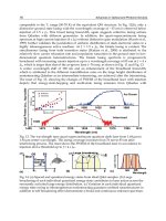
(a) (b)
Fig. 19. The probe tip touches down the membrane of sensor (a) actual experiment (b) CCD
camera.
5. Conclusion
Probe cards play an extremely important role in the semiconductor industry. In this study,
we designed a CMOS piezoresistive force sensor to be applied to the probe cards. Capable of
simultaneously monitoring the probe reacting force and electrical signals, the designed
sensor can help operators immediately identify a broken or a deformed probe and recognize
that the received signals are erroneous. The repair time and cost of the probes can therefore
be reduced. Further, we adopted the TSMC 0.35 µm 2P4M process to fabricate the CMOS
force sensor that can be integrated with the circuit. According to the measurement results,
the designed sensor reports an average sensitivity of 3.114 mV/MPa/V and a load-bearing
capacity ranging from 0 to 3 g.
6. Acknowledgements
The author would like to thank C.C.P. Contact Probes Co., Ltd. for their help. We also thank
the Chip Implementation Center of the National Science Council, Taiwan, R.O.C., for
supporting the TSMC 0.35um CMOS process. The fund is granted from NSC 94-2622-E-027
-047 -CC3.
7. References
Iscoff, R. (1994). What’s in the cards for wafer probing, Semiconductor. Int., June 1994, pp. 76
Gilg, L. (1997). Know good die, Journal of Electronic Testing: Theory and Applications, vol.
10, issue 1-2, April 1997, pp. 2019, ISSN:0923-8174
Ghalichechian, N.; Khbeis, M.; Ma, Z.; Moghadam, S. & Tan X. (2002). Piezo-resistor
pressure sensor cluster, ENEE605 Final Project Report, Fall 2002 Department of
Electrical and Computer Engineering Group #2, University of Maryland
Malhair, C. & Barbier, D. (2003). Design of a polysilicon-on-insulator pressure sensor with
original polysilicon layout for harsh environment," Thin Solid Films, vol. 427, issues
1-2, 3 March 2003, pp. 362-366, ISSN 0040-6090
Sensors, Focus on Tactile, Force and Stress Sensors
52
Yang, L. J.; Lai, C. C.; Dai, C. L. & Chang, P. Z. (2005). A piezoresistive micro pressure sensor
fabricated by commercial DPDM CMOS process, Tamkang Journal of Science and
Engineering, vol. 8, no. 1, 2005, pp. 67-73
Peng, C. T.; Lin, J. C.; Lin C. T. & Chiang, K. N. (2005). Performance and package effect of a
novel piezoresistive pressure sensor fabricated by front–side etching technology,
Sensors and Actuators A: Physical, vol. 119, 2005, pp. 28-37, ISSN 0924-4247
Wang, H. H. & Yang, L. J. (2006). Micro pressure sensors of 50μm size fabricated by a
standard CMOS foundry and a novel post process, MEMS 2006, pp. 22-26, Turkey,
22-26 January, Istanbul
Wilson, L. (1999). The National Technology Roadmap for Semiconductor, Semiconductor
Industry Association, San Jose, California, November, 1999
Smith, C. S. (1954). Piezoresistance effect in germanium and silicon, Physical Review, vol. 94,
issue 1, April 1954, pp. 42-49
Petersen, K. E. (1982). Silicon as a Mechanical Material" Proceedings of The IEEE., vol. 70, no.
5, May 1982, pp. 420-457
Thurston, R. N. (1964). Use of semiconductor transducers in measuring strain, accelerations,
and displacements, Physical Acoustics, vol. 1, pt. B. New York: Academic Press,
1964, pp. 215-235
Kanda, Y. (1982). A graphical representation of the piezoresistance coefficients in silicon,
IEEE Transactions on Electron Devices, vol. ED-29, no. 1, January, pp. 64-70
French, P. J. (2002). Polysilicon:a versatile material for microsystems, Sensors and Actuators
A: Physical, vol. 99, 20 January 2002, pp. 3-12
The CIC CMOS MEMS Design Platform for Heterogeneous Integration, Chip Implementation
Center, CIC, Taiwan, Document no. CIC-CID-RD-08-01, April 2008
Seto, J. Y. W. (1976). Piezoresistive properties of polycrystalline silicon, Journal of Applied
Physics, vol. 47, no. 11, November 1976, pp.4780-4783
4
Three-Dimensional Silicon Smart Tactile Imager
Using Large Deformation of Swollen Diaphragm
with Integrated Piezoresistor Pixel Circuits
Hidekuni Takao and Makoto Ishida
Toyohashi University of Technology
Japan
1. Introduction
Recently, various kinds of tactile sensors have been investigated and reported for tactile
applications with robot fingertips. Typical specifications of human fingertips are known as
follows; spatial resolution of human fingertip is around 1 mm, time resolution is below 1
msec (1 kHz), and the minimum force resolution is around 1-10 mN. Also, human fingertip
can recognize the three-dimensional (3-D) shape of touching object using flexible
deformation in the convex shape of fingertip skin. However, it is very difficult to realize all
the above requirements/performances in conventional tactile sensors at the same time.
Tactile imager is a spatial distribution type of sensor, which can detect the object contact
force and its distribution with an array of force or pressure sensors. In addition, detection
ability of 3-D surface shape will be required for object handling. Tactile imagers can be
applied to robot applications such as in robots for the assistance of visually handicapped
and so on. There are two major trends in the previously reported tactile imagers. One is the
polymer-based tactile imager realized by the substrate with organic materials, and the other
one is silicon-MEMS type sensors. In polymer-based tactile imagers (Brussel & Belien, 1986;
Engel et al., 2003; Shimojo et al., 2004; Someya et al., 2004, Engel et al., 2005), pressure-
sensitive conducting rubber has generally been used as a major force sensing element
(Brussel & Belien, 1986; Shimojo et al., 2004; Engel et al., 2005). Polymer-based sensors are
suitable for wide area tactile sensors since the fabrication cost per unit area is considered to
be much lower than that of silicon sensors. Artificial skin mounted on large areas of robot
surface is one of the major applications (Someya et al., 2004; Engel et al., 2005). Essential
disadvantages of polymer-based sensors are relatively low spatial resolution and upper
limitation on the number of pixels due to electronic signal wires. Typical spatial resolution
of polymer-based tactile imagers is around 2 ~ 4 mm range, which is not high enough for
fingertip tactile sensing applications as mentioned below. Although a tactile imager with a
large number of pixels has been reported using organic-FET switching matrix (Someya et al.,
2004), it still utilizes conducting rubber sensor elements. Also, the integration density of
organic-FET is much lower than the present silicon technology, and its long term reliability
in force sensor applications has not yet been demonstrated.
Silicon-MEMS tactile imagers, integrating micro pressure sensor array (Sugiyama et al.,
1990) or micro force-sensor array, have been reported earlier (Suzuki et al., 1990(a); (b);
Sensors, Focus on Tactile, Force and Stress Sensors
54
Kobayashi et al., 1990; Souza & Wise, 1997; Mei et al., 1999; Mei et al., 2000; Sato et al, 2003;
Charlot et al, 2004). This type of sensors can reduce the number of electronic signal wires by
integrated switching matrix fabricated using CMOS technology (Doelle et al, 2004). Also,
processing circuits can be integrated for front-end signal processing of the pixel array. As
compared to the polymer-based tactile imagers, a higher spatial resolution can be realized
using silicon micromachining. 500 dpi spatial resolution has already been reported (Souza &
Wise, 1997), and such sensors with high spatial resolutions can be used for fingerprint
identification (Sato et al., 2003; Charlot et al., 2004). Most of the silicon tactile imagers are
configured as integrated array of individual micromechanical sensor structures.
Piezoresistive or capacitive sensors are fabricated in each pixel structure. Since movable
stroke of such micro pixels is usually very short (~1µm), it is difficult to realize flexible
sensor surface to detect 3-D surface shape of touching object. In order to solve the problem,
thick and protective layer of elastomer can be coated on the sensor array. However, such
soft materials usually have nonlinearity due to creep and hysteresis in mechanical response.
In addition, thick and soft layer works as spatial low-pass filter for the high density pixel
array, which degrades the spatial resolution of original sensors. Although silicon-MEMS
tactile sensors can realize higher spatial resolution, it is difficult to realize surface flexibility.
Fig. 1. A future image of tactile imager embedded in robot fingers. They will function as
artificial tactile sense of fingertips in human-coexistence type robots.
Considering the tactile sensing in human-coexistence type robots, tactile imagers like human
fingertip will be required in near future. Figure 1 shows an image of tactile imager
embedded in robot fingers. The embedded imagers will function as artificial tactile sense of
fingertips in human-coexistence type robots. In human fingertips, a large number of highly
sensitive tactile corpuscles are distributed under skin, and their surface has flexibility for
object contact. As explained, it is difficult for previously reported tactile imagers to satisfy
the requirements for fingertip applications. In this study, a novel concept of silicon-MEMS
tactile imager aimed at fingertip tactile application and the evaluation results of a fabricated
device are presented. The final target is multi-functional integrated tactile imager with force,
temperature, and vibration sensing elements in sensor arrays as shown in Fig. 1, since
silicon technology is very suitable to integrate many kinds of functional sensors/circuits. In
this concept, pneumatically swollen single silicon diaphragm integrated with a two-
dimensional (2-D) array of strain-sensitive resistors (piezoresistors) is used for tactile sensor
Three-Dimensional Silicon Smart Tactile Imager Using Large Deformation of
Swollen Diaphragm with Integrated Piezoresistor Pixel Circuits
55
array instead of individually separated micromechanical sensor array. This structure has
both the large number of pixels and surface flexibility for 3-D object contact (Takao et al.,
2004; 2006). The surface shape similar to the diaphragm mechanical stroke can be detected
as 3-D information (2-D position in array and depth information). In addition, spatial
resolution higher than the polymer-based tactile imagers can be realized. A single tactile
sensor with air pressure control has been proposed earlier to detect object hardness
(Hasegawa et al., 2003). Air pressure is used to realize elastic surface and mechanical
controllability of the surface of sensing area. In this chapter, the new concept, principle,
design and experiments are presented in detail.
2. Configuration of tactile imager with silicon-LSI
2.1 A new concept of flexible silicon tactile Imager
In order to realize large mechanical stroke of tactile imager, this device concept uses large
deformation of silicon diaphragm. Figures 2 (a) and (b) show schematic diagrams of the
silicon tactile-force imager proposed in this study. It consists of three major components; (1)
silicon diaphragm with sensing pixel array for contact force imaging, (2) signal processing
circuitry integrated with IC technology, and (3) pressure chamber under the sensing
diaphragm. 2-D piezoresistor pixel array is integrated on the thin silicon diaphragm. Each
(a)
(b)
Fig. 2. Schematic diagrams of the tactile imager with skin-like sensing area; (a) Diaphragm
backside pressure is equal to atmosphere pressure, (b) Diaphragm is swollen by a pressure,
and set in the detection mode of tactile sensing.
Touching ObjectTouching Object
Air-Pressure
(Repulsive Force)
Air-Pressure
(Repulsive Force)
Signal Processing
Integrated Circuit
Signal Processing
Integrated Circuit
Through Hole
Si
Local-Relaxation of
Tensile Stress
Input ForceInput Force
Silicon Diaphragm with
Integrated Sensing Pixel Array
Atmosphere PressureAtmosphere Pressure
Bonded Glass
Pressure Chamber
Signal Processing
Integrated Circuit
Signal Processing
Integrated Circuit
Sensors, Focus on Tactile, Force and Stress Sensors
56
strain-sensor pixel is electrically isolated, but, is not isolated mechanically, since all the
pixels are formed on a continuous thin diaphragm structure. Switching and signal
processing circuits for the sensing pixel array are monolithically integrated around the
sensing diaphragm region. Pressurized air is provided to the chamber through the hole in
the glass in order to apply the pressure to the diaphragm backside. In Fig. 2 (a), pressure on
the diaphragm backside is equal to the atmosphere pressure, and the diaphragm is kept flat.
If pressurized air is applied to the diaphragm backside, the diaphragm is deformed and
swollen upward like a balloon as shown in Fig. 2 (b). Displacement of the swollen
diaphragm depends on the dimensions and applied pressure, and a movable stroke of
around 10~200 µm can easily be realized in this approach. Advantages of the tactile imager
with pneumatically swollen single diaphragm structure are summarized below.
a. Flexibility of the sensor surface is obtained without any elastomeric materials for high
spatial resolution. Convex shape of the swollen surface makes it easier to contact with
the sensing target like human’s fingertips.
b. Swollen large diaphragm can realize large stroke of surface indentation. 3-D surface
shape can be detected by measuring the indentation depth (force) of the swollen
diaphragm surface.
c. Pixel pitch of the strain sensor array can be made smaller compared to the polymer-
based sensors. In addition, number of pixels in the sensor array can be larger with
processing ability of the integrated circuits.
d. Stiffness of the sensing region of diaphragm can be controlled by the backside pressure.
This means that characteristics of the sensor can be controlled even after the device
packaging is completed (Fig. 2(b)).
2.2 Principle of 3-D Tactile Imaging
In this sensor, contact force image corresponding to 3-D image of the surface shape is
detected by reading the stress distribution change on the swollen diaphragm using the 2-D
piezoresistor pixel array. Figure 3 shows a cross-sectional view of the detection principle of
this tactile imager. The number of piezoresistor pixel array and the pixel pitch can be
changed in alternative designs. It mainly depends on the feature size of CMOS fabrication
technology used. In the initial state, before the object contact, shown in Fig. 3 (a), tensile
membrane stress is distributed with uniform amplitude over the entire piezoresistor array
on the diaphragm. Since the swollen silicon diaphragm has a finite thickness, bending stress
is generated in addition to the tensile membrane stress on the diaphragm. The surface stress
on diaphragm appears according to the principle of superposition of the two components.
Tensile membrane stress is caused by the large deformation of diaphragm, and bending
stress is caused by the bending moment proportional to the distance from the neutral plane
in the diaphragm. If the backside pressure is high, bending stress is negligible as compared
to tensile membrane stress (i.e. initial stress on the array can be regarded as uniform value).
However, the ratio between the membrane stress and the bending stress becomes only 5 or
less depending on the backside pressures in the case of 10 µm diaphragm thickness. In order
to cancel out the offset distribution caused by the effect of bending moment, they are once
memorized, and subtracted from the output for zero point adjustment. This operation can
be performed by software in the measurement system.
Figure 3 (b) shows the sensing mode of contact force of the object. If a hard object touches
the surface of the sensing region, swollen diaphragm is deformed at the object contacting
Three-Dimensional Silicon Smart Tactile Imager Using Large Deformation of
Swollen Diaphragm with Integrated Piezoresistor Pixel Circuits
57
points as shown in Fig. 3 (b). Diaphragm region where the object is in contact is pushed
downward, and the tensile membrane stress applied initially around the contacting object is
eased and reduced by the local deformation causing compressive bending stress around the
contacting points. Difference of stress distribution from the initial state corresponds to the
signal of the tactile imager, and it can be read out from the 2-D piezoresistor pixel array
sequentially. Also, the image corresponds to the depth distribution of the touching object.
Thus, the signal component shows peaks at around the tips of contacting object, and the
positions and amplitudes of force (i.e. indentation depth) on the diaphragm can be detected
as 3-D shape image of the touching object based on this principle.
Electronic Wire
Strain-Gauge Pixel Array
MOS-LSI
Signal
Processing
Positive Air-Pressure
Glass
Passivation
Bulk
Si
Signal
Processing
Glass
Touching Object
Max. Stress Change
Bulk
Si
Signal
Processing
Glass
Touching Object
Max. Stress Change
Bulk
Si
(a) (b)
Fig. 3. Detection principle of the tactile imager with surface stress distribution on the
diaphragm; (a) Initial state before object touching, (b) 3-D shape detection with deformation.
0
1
2
3
4
5
0 10203040506070
t = 3µm
5µm
10µm
20µm
Surface Compliance of Diaphragm
[µm/mN]
Diaphragm Backside Pressure [kPa]
Simulated Results
Fig. 4. Simulated surface compliance of pneumatically swollen single-crystal silicon
diaphragm for various thicknesses. FEM non-linear analysis was performed for simulations.
Mechanical properties of the sensing diaphragm can be controlled by changing the backside
air pressure. For example, compliance of the swollen diaphragm strongly depends on the
backside pressure. Finite Element Method (FEM) non-linear analysis was performed to
analyze the mechanical property of swollen diaphragm using ANSYS
®
. Total area of the
simulated diaphragm is 3040×3040 µm
2
, and the edges are fixed to the silicon substrate like a
structure shown in Fig. 2 (a). Figure 4 shows a simulated relationship between the surface
compliance of diaphragm and backside air pressure for various diaphragm thicknesses.
Sensors, Focus on Tactile, Force and Stress Sensors
58
Force is applied at a point on the diaphragm surface in the FEM simulation. If the thickness
of diaphragm increases, dependence of the surface compliance on the backside pressure
becomes small due to its own rigidity as seen in the figure. It is considered from the result
that thinner diaphragm is advantageous for controlling the characteristics of tactile imager.
Assuming that the thickness of diaphragm is same, higher sensitivity can be obtained with
lower backside pressure since the surface stiffness becomes lower and surface stress change
will be increased for the same contact force. Conversion factor from the input force into
stress change on a pixel is a dominant factor in the force sensitivity of tactile imager. On the
other hand, upper limit of the detectable force can be increased by the increased backside
pressure. Simulated dependence of the sensitivity and input force range on the pressure are
compared with the measured results in a later section.
Spatial resolution of the contact force distribution cannot be determined only by the pitch of
piezoresistors. Since the pixels are not mechanically isolated from each other, there is some
crosstalk of strain among piezoresistor pixels. If the pixel pitch of piezoresistors is shorter
than the effective limit of mechanical crosstalk, spatial resolution of the tactile imager is
limited by the crosstalk effect. FEM non-linear analysis was performed to estimate the
crosstalk between the multiple force input positions. Figure 5 (a) shows the parameters used
in the simulation. Diaphragm size used in the FEM simulation is the same as in the case of
Fig. 4 (3040×3040 µm2). Simulation was performed for different distances ‘d’, of two input
forces, varying from 120 µm to 1200 µm. In order to evaluate the spatial resolution, stress
change from the initial state (signal component) generated by the two forces is plotted as a
function of distance from the center of two forces as shown in Fig. 5 (b). In the simulation
result, amplitude of the applied forces is 5 mN, thickness t is 10 µm, and the backside
pressure is 30 kPa. This simulation corresponds to the evaluation of two-point
discrimination ability of the tactile imager. A parameter of mechanical crosstalk between the
two input points is introduced as ‘crosstalk ratio’ for quantitative evaluation of the spatial
resolution. It is determined as a ratio of generated stresses between the input point and the
center of the input points when the amplitudes of two input forces are equal. Here, the
‘crosstalk length’ is determined as the distance at which the crosstalk ratio becomes 0.5. As
seen in Fig. 5 (b), the crosstalk ratio becomes approximately 0.5 at 360 µm distance for the
boundary condition. If the length d is shorter than 360 µm, crosstalk ratio becomes higher
than 0.5. Each peak value at force input point is significantly enhanced by the signal
crosstalk, and it is difficult to distinguish the two points of force input. 360 µm is
considered as the ‘crosstalk length’ in this simulation condition. The crosstalk ratio was
almost independent of the input force in the simulated range from 0.5 to 15 mN, since it is
determined as the ratio of generated stress. On the other hand, the crosstalk ratio has
dependence on the backside pressure and diaphragm thickness. If the backside pressure is
increased from 30 kPa to 60 kPa, crosstalk ratio is improved by 18.6 % since the
deformation around the contact point becomes more local. In this case, the crosstalk
length is shortened to below 300 µm. If the thickness of diaphragm is reduced from 10 µm
to 5 µm, the crosstalk length of approximately 250 µm can be obtained at 30 kPa backside
pressure.
The crosstalk length is a function of both the diaphragm dimensions and the backside
pressure. Spatial resolution of the tactile imager is determined either from the crosstalk
length or the pixel layout pitch of piezoresistor array.
Three-Dimensional Silicon Smart Tactile Imager Using Large Deformation of
Swollen Diaphragm with Integrated Piezoresistor Pixel Circuits
59
Diaphragm
Surface
Backside Air Pressure
d [µm]
Center of Two
Input Forces
Force 1
Force 2
Uniformly Distributed Repulsive Forces
Diaphragm
Thickness
T [µm]
Backside Pressure
(a)
-1.6 10
8
-1.4 10
8
-1.2 10
8
-1 10
8
-8 10
7
-6 10
7
-4 10
7
-2 10
7
0
-1200 -900 -600 -300 0 300 600 900 1200
d = 120µm
240µm
360µm
480µm
600µm
720µm
840µm
1200µm
Signal Component of Stress Change [N/m
2
]
Distance from Center of Two Input Forces [µm]
Force Input Points
(b)
Fig. 5. FEM simulation for spatial resolution analysis; (a) Model parameters in the FEM
analysis for the estimation of mechanical crosstalk between two input forces,
(b) Distribution of stress signal component generated by the two input forces for various
distances of d. The backside pressure is 30 kPa.
As discussed in this section, the backside pressure of the diaphragm influences both the
spatial resolution and the sensitivity for contact input forces. A comparison of FEM results
simulated at different pressures is helpful to understand this relationship. Figure 6 (a) and
(b) show the simulated stress change (signal component) distributions on a sensing
diaphragm of this tactile imager at 23.0kPa and 5.0kPa, respectively. A half model of the
sensor structure is used. A load of 8.5mN is applied at the contact point in the figure. In the
case of 23.0kPa (Fig. 6 (a)), stress change is distributed locally around the contact point. On
the other hand, both the stress level and strained area are increased in the 5.0kPa case as
shown in Fig. 6 (b). This means that reduction of the backside pressure results in both
Sensors, Focus on Tactile, Force and Stress Sensors
60
improvement of sensitivity (i.e. SNR) and degradation of spatial resolution for an input
force applied. Selecting a proper backside pressure adaptively for the device dimensions
and expected input force range, the maximum SNR of the tactile imager can be obtained for
a required spatial resolution (crosstalk length).
Contact Point
Contact Point
(a) (b)
Fig. 6. Simulated stress change (signal component) distributions on a sensing diaphragm of
this tactile imager; (a) Backside pressure is 23.0kPa; (b) Backside pressure is 5.0kPa.
3. Device design and fabrication
3.1 Design of piezoresistor pixel circuit on diaphragm
Signal component of the stress, generated by the object contact, is translated into voltage
signal in each pixel circuit with piezoresistor. Figure 7 (a) shows the circuit configuration of
each pixel on the diaphragm. A pixel includes n-type diffused piezoresistor for the detection
of surface stress (R
PR
), n
+
-poly Si reference resistor with very small stress sensitivity (R
poly
),
logic gates for pixel select operation (NAND and NOT), and switch MOSFETs for resistor
drive current (M1) and pixel output (M2). Tensile membrane stress generated strongly on
the swollen diaphragm is almost isotropic, and the shear component of stress on each pixel
is almost zero. Select terminals of line (X_Sel) and column (Y_Sel) of pixel circuits in the
array is driven sequentially in order to read out the distribution of output voltage. If both
X_Sel and Y_Sel in the pixel are pulled up to V
dd
, switches M1 and M2 are turned on, and
drive current for R
PR
and R
poly
is provided from the power source through M1. The
piezoresistor R
PR
translates the surface stress level on each pixel into a corresponding
resistance value. Voltage of the output line is determined as a partial voltage of R
PR
and R
poly
since M2 is turned on in this case. The output voltage of pixel (V
Pix_Out
) fed to the common
amplifier in the following stage is expressed by the next equation (Takao et al, 2006);
)(
)(
2
_ SSDD
PolyPR
Poly
AmpM
Amp
PolyPR
SSDDPoly
OutPix
VV
RR
R
RR
R
RR
VVR
V −⋅
+
=
+
⋅
+
−
⋅
≈
[V] (1)
where R
Amp
is equivalent input impedance of the common amplifier (dashed line in the
figure), and R
M1
and R
M2
are on-channel resistances of M1 and M2, respectively (Takao et al.,
2006). In this situation, M1 and M2 are operating in non-saturation region at gate voltage of
V
dd
, and its channel resistance is much lower than the other resistances (i.e. R
M1
<< R
PR
, R
poly
Three-Dimensional Silicon Smart Tactile Imager Using Large Deformation of
Swollen Diaphragm with Integrated Piezoresistor Pixel Circuits
61
and R
M2
<< R
Amp
). Assuming that only the planar components of surface stress in parallel to
the diaphragm surface is dominant, resistance of a piezoresistor can be expressed with a
simplified linear expression with the products of piezoresistive coefficient and applied
stress. If n-type piezoresistor in the pixel is integrated on Si(100) and oriented to a direction
equivalent to <110>, longitudinal and transversal components of piezoresistive coefficient
become equal (i.e.
π
long
=
π
trans
= π
n<110>
) (Kanda, 1982). Resistance value of R
PR
under tensile
membrane stress can be expressed as the following expression considering the isotropic
distribution of stress on the swollen diaphragm;
X_Sel
Y_Sel
V
Pix_Out
V
dd
V
ss
n-type diffused
Piezoresistor
R
PR
R
Poly
poly-Si
reference
resistor
M1
M2
NAND
NOT
R
Amp
Output Line
X_Sel
Y_Sel
V
Pix_Out
V
dd
V
ss
n-type diffused
Piezoresistor
R
PR
R
Poly
poly-Si
reference
resistor
M1
M2
NAND
NOT
R
Amp
Output Line
(a)
I
SUP
·π
n<110>
·k · dF
Pix
R
Poly
R
PR_0
dV
Pix_Out
dF
Pix
+
–
+
–
Force Input
Pixel Output
Small Signal Equivalent Circuit for Force Input
(b)
Fig. 7. An example of pixel circuit design including a piezoresistor; (a) Circuit configuration
of a unit pixel, (b) Small signal equivalent circuit of the pixel for a force input signal.
)1()1()(
1100_0_ EQnPRtranstranslonglongPRPR
RRR
σ
π
σ
π
σ
π
σ
><
+
⋅
=
+
+
⋅
≈
[Ω]
(2)
where R
PR_0
is the resistance of R
PR
under zero-stress condition, and
σ
EQ
is an equivalent
value of stress corresponding to the sum of the two-axis components of average stress
distributed on piezoresistor in a pixel. Typical values for
π
n<110>
are around 10
-10
m
2
/N and
its polarity is negative. Stress sensitivity of the output voltage in the pixel can be derived by
partial differential on
σ
EQ
;
Sensors, Focus on Tactile, Force and Stress Sensors
62
PolyPR
RRSUPn
PolyPR
PolyPR
SSDDn
EQ
OutPix
Pix
RI
RR
RR
VV
V
S
//110
2
0_
0_
110
_
_
0_
)(
)( ⋅⋅−=
+
⋅
⋅−⋅−≈
∂
∂
=
><><
ππ
σ
σ
[V/(N/m
2
)] (3)
where R
RPR_0//RPoly
is the combined resistance of parallel connection of R
PR_0
and R
Poly
, and
I
SUP
is the initial supply current to R
PR
and R
Poly
. Assuming a linear relationship between
average stress change on a pixel and average contact force applied on the pixel area, force
sensitivity of the pixel can be expressed as small signal sensitivity in the following
expression;
kIR
dF
dFkS
dF
dS
dF
dV
S
nSUPRR
Pix
PixPix
Pix
EQPix
Pix
OutPix
FPix
PolyPR
⋅⋅⋅−=
⋅
⋅
=
⋅
==
><110//
___
_
0_
π
σ
σσ
[V/N] (4)
where d
σ
EQ
= k · dF
Pix
, and k is the conversion factor from the input force (dF
Pix
) into signal
component of stress change on the pixel (d
σ
EQ
) discussed in the section 2.2. The conversion
factor strongly depends on the stiffness of diaphragm surface (i.e. backside pressure).
Output signal of a pixel is expressed as a product of S
Pix_F
and input force.
Figure 7 (b) shows the small signal equivalent circuit of a piezoresistor pixel corresponding
to the above relationship between the input force and pixel output. Reading the output
signal obtained from sensing pixels in the array, contact force image on the diaphragm can
be obtained as two-dimensional distribution. It is easily derived from the simple analysis of
the partial differential of pixel sensitivity on R
PR
that the maximum sensitivity is obtained if
the condition R
PR
= R
Poly
is satisfied in the real device. Resistance values of R
PR_0
and R
Poly
are
decided from the power consumption point of view for a fixed power supply voltage and
pixel area, while the ratio of resistances should be controlled to bring it close to 1.0 for high
sensitivity.
3.2 Layout design of the overall sensor chip
A prototype device with a small scale integrated sensor array was designed and fabricated.
The die size of the designed sensor is 5200 × 5200 µm
2
, and the sensing diaphragm region
with integrated pixel array is 3040×3040 µm
2
. 5.0µm technology design rule was used in the
pixel circuit design, and the size of pixel layout equivalent to Fig. 7 (a) became 420 × 420
µm
2
. R
PR
and R
Poly
were designed to be 3 kΩ in the pixel layout. In the prototype device, 6 ×
6 sensing pixel array was designed on the sensing diaphragm considering the pixel size
(pitch) and the diaphragm size. The sensor array occupies an area of 2520 × 2520 µm
2
on the
diaphragm. Tensile membrane stress becomes quite uniform over the array area, and the
effect of fixed diaphragm edge, estimated by FEM simulation, is below 10 % in the area. On
the peripheral of the diaphragm region, signal conditioning circuits for sensing operation
were designed. It includes array scanning logic circuits for sequential readout of pixel array
outputs, a reference signal generator for differential readout of each pixel output.
Diaphragm area in the device is same as in the simulated model discussed in section 2.2.
Thickness of the sensing diaphragm of the device was decided considering some
parameters. A thinner diaphragm is advantageous to a thicker one for controllability of the
mechanical property with air pressure as shown in Fig. 4. Also, the thinner the diaphragm,
the higher the spatial resolution as discussed in section 2.2. Considering the advantages,
designed pixel size of 420 µm, and some difficulties in fabrication process, the thickness was
decided to 10 µm. The spatial resolution of the designed device is considered to be
Three-Dimensional Silicon Smart Tactile Imager Using Large Deformation of
Swollen Diaphragm with Integrated Piezoresistor Pixel Circuits
63
approximately equal to the pixel size in this design, since the crosstalk length becomes 360
µm at 30 kPa for 10 µm-thick diaphragm, which is shorter than the pixel pitch, 420 µm. If the
backside pressure is reduced to below 18 kPa, spatial resolution will be limited by the
increased crosstalk length instead of the pixel pitch.
Calculated displacement of the diaphragm at the center is 31.8µm for 30 kPa, and 48.6 µm
for 100 kPa backside pressure. Although, the mechanical stroke is too short to apply it to
fingertip tactile sensor application, flexibility of the sensor surface is much higher than the
conventional silicon-MEMS tactile imagers. The movable distance can be increased using
larger and thinner diaphragm structure.
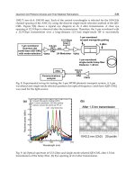
3.3 Device fabrication from standard LSI wafers
The designed device was fabricated with our silicon IC/MEMS fabrication technology
(Takao et al., 1997; 1999; 2001). Figure 8 shows outline of the fabrication process. 1) Starting
material of the tactile imager was 2-inch and 300 µm-thick p-type Si (100) wafer with
resistivity of 1~3 Ω. 2) 6 × 6 Sensing pixel array including piezoresistors and signal
processing circuits were fabricated. 3) After the electrical check of the circuits, surface of the
integrated circuit was protected by 6 µm-thick polymer layer (CYTOP®) to prevent physical
damage in the following bulk-etching process (Takao et al., 1997). The diaphragm etching
pattern was defined by SiO
2
layer using wafer backside aligner. 4) Silicon substrate was
etched by 25-wt% TMAH solution at 90 ºC for 6.5 hours using the SiO
2
masking layer. In this
step, silicon thickness of the sensing diaphragm region was controlled to 10 µm ± 1 µm by
etching time control. Variation of thickness in a diaphragm was within 0.5 µm. 5) The
protective layer on the surface was removed, and a glass substrate with through holes was
bonded to the backside of silicon wafer by adhesive bonding with epoxy glue.
1)
2)
4)
5)
3)
300µm-thick Si (100) wafer300µm-thick Si (100) wafer
p-type 1~3 Ω-cm
6×6 Pixel ArrayIntegrated Circuits
Thermal-SiO
2
Layer
Protective Layer (CYTOP)
SiO
2
Masking Layer for TMAH Etching
25-wt% TMAH25-wt% TMAH
Protective Layer (CYTOP)
Through Hole
Glass Substrate
Epoxy Glue
Fig. 8. Fabrication process; 1) Starting material of the tactile imager, 2) Fabrication of 6 × 6
Sensing pixel array including piezoresistors and signal processing circuits, 3) Protection of
the circuit surface by a polymer layer (CYTOP
®
) and definition of the diaphragm etching
pattern, 4) Backside-wafer etching with 25-wt% TMAH solution at 90 ºC, 5) Removal of the
protective layer on the surface and bonding to the glass substrate with epoxy glue layer.
Sensors, Focus on Tactile, Force and Stress Sensors
64
Figure 9 (a) shows a photograph of the fabricated tactile imager with 6 × 6 pixel array
integrated on a diaphragm structure. Close-up photograph of a pixel circuit corresponding
to Fig. 7 (a) is shown in Fig. 9 (b). In the pixel, n-type piezoresistor device has a box-like
shape to detect isotropic stress on the swollen diaphragm effectively, since n-type
piezoresistor on Si(100) has bi-axial sensitivity. The areas of the piezoresistor and n
+
-poly Si
reference resistor are indicated in the figure.
Sensing Diaphragm Region
with 6×6 Sensor Pixel Array
X1 X2 X3 X4 X5 X6
Y1
Y2Y3Y4
Y5Y6
1mm
Reference
Poly-Si
Resistor
Piezoresistor
Area
420 µm
(a) (b)
Fig. 9. Photograph of a fabricated tactile imager with 6 × 6 pixel array integrated on the
diaphragm; (a) Overall Chip, (b) Close-up of a pixel circuit in the 6 × 6 pixel array.
4. Characteristics evaluation
4.1 Single point contact force detection
Device characterization was performed with the experimental setup shown in Fig. 10 (a).
The fabricated sensor was fixed on a three-axis (X-Y-Z) stage with position resolution of 1
µm in order to control the contact position and input force of measured object on the sensing
Signal
Recording
System
Tactile
Sensor
Contacting
Object
X-Axis
Z-Axis
Y-Axis
BASE
Pressure
Pump
&
Regulator
Micro-Force
Gauge
3-Axis Stage
Fixed
(a) (b)
Fig. 10. Experimental setup; (a) Total system for device characterization; (b) Photograph of a
sensing diaphragm deformed by a touching object.
Three-Dimensional Silicon Smart Tactile Imager Using Large Deformation of
Swollen Diaphragm with Integrated Piezoresistor Pixel Circuits
65
diaphragm. A micro-force gauge with 0.5 mN resolution was used to measure the total
contact force of measured object on the sensor surface. Controlled air pressure was applied
to the diaphragm backside using a pumping system and a pressure regulator. Signal
obtained from the sensor chip was recorded with external measurement equipment and PC.
Fig. 10 (b) shows a photograph of the sensing diaphragm deformed by a touching object.
Deformation of the diaphragm surface and the indentation can be easily recognized by the
reflection of light on the sensing area.
X
X
Y
Y
(X, Y) = (4, 3)
5 mm
Diaphragm Swollen at 23 kPa
(a)
X
1
0
4
8
X
2
X
3
X
4
X
5
X
6
Y
1
Y
2
Y
3
Y
4
Y
5
Y
6
O
u
t
p
u
t
V
o
l
t
a
g
e
[
m
V
]
X
1
0
4
8
X
2
X
3
X
4
X
5
X
6
Y
1
Y
2
Y
3
Y
4
Y
5
Y
6
O
u
t
p
u
t
V
o
l
t
a
g
e
[
m
V
]
X
1
X2
X3
X4
X5
X6
Y1
Y2
Y3
Y4
Y5
Y6
0
4
8
O
u
t
p
u
t
V
o
l
t
a
g
e
[
m
V
]
X
1
X2
X3
X4
X5
X6
Y1
Y2
Y3
Y4
Y5
Y6
0
4
8
O
u
t
p
u
t
V
o
l
t
a
g
e
[
m
V
]
(b) (c)
Fig. 11. (a) Photograph of evaluation experiment using a plastic tip with a width of
approximately 1mm. The plastic tip is contacting at around (X4, Y3) address in 6×6 array at
29 mN, (b) Measured output voltage mapping of the fabricated prototype device in the case
the plastic tip is contacting at around (X4, Y3), (c) Measured output voltage mapping in the
case the plastic tip is contacting at around (X2, Y4).
First, the detection ability of single point contact was evaluated. Figure 11 (a) shows the
photograph of evaluation experiment using a plastic tip with gentle point as the contacting
object. In the photograph, the tip is contacting on a pixel around (X4, Y3) address in 6 × 6
sensor array. A 23.0kPa pressure was applied to the diaphragm backside, and the plastic tip
was put on a pixel on the sensing diaphragm with 29mN-force. Movable stroke of the
swollen diaphragm from the original surface was approximately 30 µm at the center of the
diaphragm. Spatial resolution of the tactile imager is the pixel pitch of 420 µm for 23.0 kPa
backside pressure as discussed in the previous section. Considering the movable stroke of
Sensors, Focus on Tactile, Force and Stress Sensors
66
the sensor surface, only a small tip area of the plastic tip is contacting on the diaphragm
surface. The width of the tip is approximately 1 mm.
Figures 11 (b) and (c) show measured output voltage mapping obtained from the tactile
imager in this experiment. In Fig. 11 (b), since the plastic tip is contacting around (X4, Y3), the
peak of the pixel output signal appears on the same address in the 3-D plot. In addition, since
the spatial resolution of the tactile imager is 420 µm, contact force applied by the gentle point
with 1 mm width is detected by the pixels around (X4, Y3). In other words, the gentle shape
wider than the spatial resolution is detected by the plural pixels in the sensor array. After the
measurement, the plastic tip was moved to another position (X2, Y4), and the output signal
obtained from the sensor is as shown in Fig. 11 (c). The peak position of output signal appears
at (X2, Y4), and the shape of peak in the output around the contacting point is similar as in the
case of (X4, Y3). Amplitude of the output peak is almost same in these two cases.
4.2 Multi-point contact and 3-D surface shape detection
Multi-point detection ability of this tactile imager was also evaluated. Figure 12 (a) shows a
photograph of the multi-point contact test arrangement using two sharp fingers of a rubber
toy. The fingers are contacting at the points of (X3, Y2) and (X4, Y5) with total load of 29
mN. The right finger contacting at (X4, Y5) is slightly longer than the left finger contacting at
Total Load 29 mN
(X3,Y2)
(X4,Y5)
2 mm
(a)
Y1 Y2 Y3 Y4 Y5 Y6
X1
X2
X3
X4
X5
X6
-4
-2
0
2
4
6
8
10
12
14
Output Voltage [mV]
Y1 Y2 Y3 Y4 Y5 Y6
X1
X2
X3
X4
X5
X6
-4
-2
0
2
4
6
8
10
12
14
Output Voltage [mV]
(b)
Fig. 12. Multi-point detection using this tactile image sensor; (a) Photograph of multi-point
contact test and the sharp point of the rubber finger. Two fingers of rubber toy are contacting
at (X3, Y2) and (X4, Y5), respectively, (b) Obtained output distribution with two signal peaks at
(X3, Y2) and (X4, Y5), that correspond to the two positions of touch of the two rubber fingers.
Three-Dimensional Silicon Smart Tactile Imager Using Large Deformation of
Swollen Diaphragm with Integrated Piezoresistor Pixel Circuits
67
(X3, Y2). As seen in the photograph, the shape of the points of the rubber fingers is much
sharper than the point of the plastic-tip shown in Fig. 11 (a). The width of the points is
approximately below 300 µm under the contacting situation, and it is smaller than the
spatial resolution of the tactile imager (i.e. 420 µm in this experiment). Distribution of the
output signal obtained from the experiment is shown in Fig. 12 (b). There are two signal
peaks at (X3, Y2) and (X4, Y5), and their positions correspond to the two contact points of
the two rubber fingers. Signal level of the peak at (X4, Y5) is larger than the peak at (X3, Y2).
This corresponds to the fact that the partial contact force of the rubber finger at (X4, Y5) is
larger than that of at (X3, Y2). In addition, the shapes of the output peaks around the
contacting positions are much sharper than the shapes obtained in Fig. 11 (b) and (c). This
fact implies that the shape of peak point in the output distribution correctly reflects the
shape of the contacting point within the limit of the spatial resolution, even though some
effect of mechanical crosstalk is seen among the pixels. Through the experiments, basic
detection ability of multiple contact forces and the spatial resolution of the tactile imager
have been demonstrated successfully.
4.3 Ability of characteristic control
Dependence of the contact force sensitivity of each pixel on the backside pressure was
evaluated using a sharp tip of rubber finger shown in Fig. 12 (a), since contacting point smaller
than the pixel size is necessary to evaluate the pixel sensitivity. Figure 13 (a) shows a measured
relationship between pixel force sensitivity of the fabricated sensor and the diaphragm
backside pressure. Supply voltage was 5 V, and piezoresistor pixel at (X3, Y4) was used in the
measurement. In the figure, sensitivity dependence on the backside pressure, calculated using
FEM, is also plotted. Since the FEM results are additionally plotted to have agreement with the
measured sensitivity at 20 kPa, only the shape of pressure dependence can be compared in this
figure. Dependence of FEM simulation results on the backside pressure are in good agreement
with the measured characteristics. Increasing the pressure, force sensitivity decreased due to
increase of repulsive force of the swollen diaphragm. The higher the pressure, the lower the
pixel force sensitivity. The force sensitivity is backside pressure dependent, whereas measured
noise floor of the pixel output is a constant value (approximately 10 µV/Hz
0.5
) and
independent of the pressure. Hence, a lower backside pressure results in a higher signal to
noise ratio (SNR), and is suitable for the detection of small amplitude of the contact force. For
example, the minimum detectable input force becomes approximately 1 mN at 2 kHz
bandwidth in the case of 60 kPa backside pressure. This result indicates that if the diaphragm
backside pressure is reduced to 5 kPa, the minimum detectable input force will be improved to
about 400µN with the same signal bandwidth.
Not only the sensitivity but also the maximum input force is dependent on the backside
pressure. If the backside pressure is too low for an input force applied to the sensor surface,
the diaphragm yields to the over load. Diaphragm surface is swollen to opposite side by a
large input force, and pixel output is finally saturated due to the bottoming of the
diaphragm deflection. A higher backside pressure is required to detect and support a larger
input force on the diaphragm even if the force sensitivity of pixel (i.e. SNR) is degraded.
Figure 13 (b) shows the measured relationships between the forced displacement of
diaphragm and pixel input force for various backside pressures. Forced displacement
calculated with FEM is also plotted in the figure. Even though there are some differences,
the results of FEM show a good agreement with the measurement results. Stiffness of the
Sensors, Focus on Tactile, Force and Stress Sensors
68
diaphragm surface increases as the backside pressure increases. It is clearly expected from
the results that the maximum input force of the tactile imager can be increased by increasing
the backside pressure. There is a tradeoff relationship between SNR and the input force
range in the tactile imager as seen in the experimental results. The lower the backside
pressure, the higher the force resolution and the lower the maximum input force. In
0.4
0.5
0.6
0.7
0.8
0.9
1
1.1
1.2
0 10203040506070
Measured Sensitivity
FEM Simulation
Pixel Force Sensitivity [mV/mN]
Diaphragm Backside Pressure [kPa]
(a)
0
10
20
30
40
50
0 10203040
Measurement @ 5kPa
Measurement @10kPa
Measurement @20kPa
FEM Simulation @ 5kPa
FEM simulation @10kPa
FEM Simulation @20kPa
Forced Displacement of Diaphragm [µm]
Input Force to a Pixel [mN]
(b)
Fig. 13. (a) Measured force sensitivity of a pixel for various diaphragm backside pressures.
Simulated sensitivities with FEM non-linear analysis are also plotted, (b) Measured
relationship between forced displacement of the diaphragm surface and input force for
various backside pressures.
Three-Dimensional Silicon Smart Tactile Imager Using Large Deformation of
Swollen Diaphragm with Integrated Piezoresistor Pixel Circuits
69
contrast, the higher the backside pressure, the lower the force resolution and the higher the
maximum input force. Figure 14 shows an example of over-range input measured with the
plastic tip used in Fig. 11. The plastic tip is contacted on (X4,Y5) pixel in the swollen
diaphragm at a force of 33mN. The backside pressure is only 4.8kPa which is insufficient for
the input. In this case, large area of the diaphragm is largely deformed downward, and
precise shape of the tip is not obtained. Once the backside pressure is increased to 23kPa,
sharp shape image of the tip is obtained, and contacting position is well recognized similarly
with Fig. 11 (b) and (c).
In conclusion, if the backside pressure is adaptively controlled for amplitudes of the input
forces, apparent dynamic range of the tactile sensor will be improved. It has been confirmed
that the maximum input force range can be controlled from 21 mN to 176 mN by changing
the backside pressure from 5 to 64 kPa using the same device (Takao et al., 2006). Even if
adaptive control of the pressure is not necessary, sensing characteristics can be chosen or
optimized by selecting the sealing pressure suitably for the estimated range of input force in
the application.
-8
-6
-4
-2
0
2
4
6
8
10
12
14
Output Voltage [mV]
X1
X2
X3
X4
X5
X6/Y1
Y2
Y3
Y4
Y5
Y6
X
-
P
o
s
i
t
i
o
n
Y
-
P
o
s
i
t
i
o
n
-8
-6
-4
-2
0
2
4
6
8
10
12
14
Output Voltage [mV]
X1
X2
X3
X4
X5
X6/Y1
Y2
Y3
Y4
Y5
Y6
X
-
P
o
s
i
t
i
o
n
Y
-
P
o
s
i
t
i
o
n
Fig. 14. An example result of over-range input measurement.
5. Conclusions and outlook
In this chapter, a novel concept of silicon-MEMS tactile imager aimed at fingertip tactile
applications and evaluation results of a fabricated device have been presented. Array of
strain-sensitive sensor pixels was integrated on a pneumatically swollen silicon diaphragm
with signal processing circuits in monolithic configuration. Elastic surface of the tactile
imager is realized using repulsive force of air pressure applied to the diaphragm backside.
Contact force distribution of an object was detected from stress distribution change on the
diaphragm. Force range and force sensitivity can be controlled by the pressure even after
device packaging step. In this principle, fine pitch of pixels and a large scale sensing array
can easily be realized using abilities of silicon CMOS technology. In addition, movable
stroke of the sensor surface can be made much longer than individually formed micro
mechanical pixels. A designed and fabricated sensor with 3040×3040 µm
2
sensing
diaphragm was fabricated integrating with a 6 × 6 array, 420µm-pitch, piezoresistor pixels.
Sensors, Focus on Tactile, Force and Stress Sensors
70
Movable stroke of the swollen diaphragm from the original surface is around 30 µm at 23
kPa pressure at the center. Realized spatial resolution of the fabricated device is
approximately 400 µm, which is determined by the relationship between the pixel pitch and
mechanical crosstalk among the pixels. The crosstalk depends on both the diaphragm
thickness and backside air pressure. Positions of touch and their contact force amplitudes
were detected as 2-D distribution of output voltage form the pixel array in multi-point
contact test. The maximum input force range can be controlled from 21 mN to 176 mN by
changing the backside pressure from 5 to 64 kPa. Through the evaluation of the fabricated
device, advantages of the new configuration of tactile imager have been demonstrated
successfully.
As introduced in Section 1, multi-functional sensing is one of future directions for tactile
imager devices. Recently, our group has presented multi-functional tactile imager with
integrated arrays of piezoresistors and temperature sensors for simultaneous detection of
force and temperature distribution images (Takao et al., 2005). Also, another group has
succeeded to realize simultaneous measurement of stress and temperature using single
field-effect transistor structure (Doelle et al., 2006). Realization of multi-functional detection
ability is a firm direction of future technology in integrated silicon smart sensor field. The
advantage of silicon technology for integration is very promising feature for highly
functional tactile imager for advanced tactile sensing applications. On the other hand, once
over-ranged strain is applied, silicon is well known as a fragile material even though it has
very good mechanical properties and large breaking stress in room temperature. Research to
realize robustness of the silicon tactile imager has just started (Takao et al., 2007), and it will
be a challenge to change silicon tactile imagers from a research target to practical sensing
devices used widely in many fields.
6. References
Brussel, H. V. &Belien, H. (1986). A High Resolution Tactile Sensor for Part Recognition,
Proc. 6
th
Int. Conf. Robot Vis. Sens. Control, pp. 49-59.
Engel, J.; Chen, J. & Liu, C. (2003). Development of polyimide flexible tactile sensor skin,
Journal of Micromechanics and Microengineering, Vol. 13, No. 9, pp. 359-366.
Engel, J.; Chen, J.; Fan, Z. & Liu, C. (2005). Polymer micromachined multimodal tactile
sensors, Sensors and Actuators A, Vol. A117, No. 1, pp. 50-61.
Shimojo, M.; Makino, R.; Namiki, A.; Ishikawa, M. & Mabuchi, K. (2004). A Tactile Sensor
Sheet Using Pressure Conductive Rubber with Electrical Wires Stitched method,
IEEE Sensors journal, Vol. 4, No. 5, pp. 589-596.
Someya, T.; Sekitani, T.; Iba, S.; Kato, Y.; Kawaguchi, H. & Sakurai, T. (2004). A large-area,
flexible pressure sensor matrix with organic field-effect transistors for artificial skin
applications, Proceedings of the National Academy of Sciences of the United States of
America, Vol. 101, Issue 27, pp. 9966-9970.
Sugiyama, S.; Kawahata, K.; Yoneda, M. & Igarashi, I. (1990). Tactile Image Detection Using
a 1k-element Silicon Pressure Sensor Array, Sensors and Actuators A, Vol. 22, No.
1/3, pp. 397-400.
Suzuki, K.; Najafi, K. & Wise, K. (1990). A 1024 element high-performance silicon tactile
imager, IEEE Transactions on Electron Devices, Vol. 37, No. 8, pp. 1852-1860.
Suzuki, K.; Najafi, K & Wise, K. (1990). Process alternatives and scaling limits for high-
density silicon tactile imagers, Sensors and Actuators A, Vol. 23, No. 1/3, pp. 915-918.
Three-Dimensional Silicon Smart Tactile Imager Using Large Deformation of
Swollen Diaphragm with Integrated Piezoresistor Pixel Circuits
71
Kobayashi, S.; Mitsui, T.; Shoji, S. & M. Esashi (1990). Two-lead Tactile Sensor Array Using
Piezoresistive Effect of MOS Transistor, Tech. Digest of the 9
th
Sensor Symposium, pp.
137-140, Tokyo, Japan, June 1990, IEEJ, Tokyo.
Souza, R. & Wise, K. (1997). A very high density bulk-micromachined capacitive tactile
imager, Digest of Tech. Papers of Transducers’97, Vol. 2, pp. 1473-1477, Chicago USA,
June 16-19, 1997.
Mei, T.; Ge, Y.; Chen, Y.; Ni, L.; Liao, W.; Xu, Y. & Li, W. (1999). Design and Fabrication of
an Integrated Three-Dimensional Tactile Sensor for Space Robotic Applications,
Proceedings of IEEE MEMS’99, pp. 130-134, 1999.
Mei, T.; Ge, Y.; Chen, Y.; Ni, L.; Li, W. J. &Chan, M. H. (2000). An integrated MEMS three-
dimensional tactile sensor with large force range, Sensors and Actuators A, Vol. A80,
No. 2, pp. 155-162.
Sato, N.; Machida, K.; Morimura, H.; Shigematsu, S.; Kudou, K.; Yano, M. & Kyuragi, H.
(2003). MEMS fingerprint sensor immune to various finger surface conditions, IEEE
Transactions on Electron Devices, Vol. 50, No. 4, pp. 1109-1116.
Charlot, B.; Galy, N.; Basrour, S. & Courtois, B. (2004). A Sweeping Mode Integrated
Fingerprint Sensor with 256 Tactile Microbeams, Journal of Microelectromechanical
Systems, Vol. 13, No. 4, pp. 636-644.
Doelle, M.; Peters, C.; Gieschke, P.; Ruther, P. & Paul, O. (2004). Two-Dimensional High
Density Piezo-FET Stress Sensor Arrays for In-Situ Monitoring of Wire Bonding
Processes, Proceedings of IEEE MEMS2004, pp. 829-832, Maastricht The Netherlands,
Jan. 25-29, 2004.
Doelle, M.; Held, J.; Ruther, P. & Paul, O. (2006). Simultaneous and Independent
Measurement of Stress and Temperature Using a Single Field Effect Transistor
Based Sensor, Proceedings of IEEE MEMS2006, pp. 150-153, Istanbul Turkey, Jan. 22-
26, 2006.
Takao, H.; Matsumoto, Y. & Ishida, M. (1997). A Monolithically Integrated Three Axial
Accelerometer Using Stress Sensitive CMOS Differential Amplifiers, Digest of
Technical Papers of Transducers '97, Vol. 2, pp. 1173-1176, Chicago USA, June 16-19,
1997.
Takao, H.; Matsumoto, Y. & Ishida, M. (1999). An Integrated Three-Axis Accelerometer
Using CMOS Compatible Stress Sensitive Differential Amplifiers, IEEE Transactions
on Electron Devices, Vol. 46, No.1, pp. 109-116.
Takao, H.; Fukumoto, H. & Ishida, M. (2001). A CMOS Integrated Three-Axis Accelerometer
Fabricated with Commercial Sub-micron CMOS Technology and Bulk-
Micromachining, IEEE Transactions on Electron Devices, Vol.48, No.9, pp.1961-1968.
Takao, H.; Sawada, K. & Ishida, M. (2004). Silicon Smart Tactile Image Sensor with
Pneumatically Swollen Single Diaphragm Structure, Proceedings of IEEE
MEMS2004, pp.846-849, Maastricht The Netherlands, Jan. 25-29, 2004.
Takao, H., Sawada, K. & Ishida, M. (2005). Multifunctional Smart Tactile-Image Sensor with
Integrated Arrays of Strain and Temperature Sensors on Single Air-Pressurized
Silicon Diaphragm, Dig. Tech. Papers of Transducers’05, pp. 45-48, Seoul Korea, June
5-9, 2005.
Takao, H.; Sawada, K. & Ishida, M. (2006). Monolithic Silicon Smart Tactile Image Sensor
with Integrated Strain Sensor Array on Pneumatically Swollen Single Diaphragm
Structure, IEEE Transactions on Electron Devices, Vol. 53, No. 5, pp. 1250-1259.
Sensors, Focus on Tactile, Force and Stress Sensors
72
Takao, H.; Yawata, M.; Sawada, K. & Ishida, M. (2007). A Robust and Sensitive Silicon-
MEMS Tactile-Imager with Scratch Resistant Surface and Over-Range Protection,
Dig. Tech. Papers of Transducers’07, pp. 1465-1468, Lyon France, June 10-14, 2007.
Hasegawa, Y.; Shimizu, T.; Miyaji, T.; Shikida, M.; Sasaki, H.; Sato, K. & Itogigawa, K. (2003).
Hardness Detection Using A Micromachined Active Tactile Sensor, Digest of
Technical Papers of IEEE Transducers’03, pp. 927-930, Boston USA, June 2003.
Kanda, Y. (1982). A Graphical Representation of the Piezoresistance Coefficients in Silicon,
IEEE Transactions on Electron Devices, Vol. ED-29, No. 1, pp. 64-70.
5
High-Sensitivity and High-Stiffness
Force Sensor Using Strain-Deformation
Expansion Mechanism
Yong Yu Takashi Chaen and Showzow Tsujio
Dept. of Mechanical Engineering, Kagoshima University, Kagoshima 890-0065,
Japan
1. Introduction
In order to grasp and manipulate an object controllably and dexterously with a
multifingered hand of robot, the sensing of fingertip force is required. To these operation,
for making the controlability higher and making force sensor be proof against unexpected
collisions or weights, not only the sensor’s sensibility but also its stiffness are desired as high
as possible.
For sensing a force acting on a force sensor, in general, some sensing elastic bodies is
equipped in the force sensor. When a force is applied on the sensor, the force will pass
through the sensing elastic bodies and make the bodies deform linearly so that it can be
measured from the strain-deformations on the elastic bodies. So far, many researches [1]∼[7]
[9] consider making the sensed force all passed through the sensing elastic bodies for force
sensing. To this situation, if we want to make the sensibility higher, the stiffness of the
sensing elastic bodies have to be reduced for making their deformations larger. Conversely,
if we wan to make the stiffness higher, the sensibility of the sensing elastic bodies will be
reduced since their deformations become to small because of the higher stiffness. Thus by
using the previous sensing structures, it is hard to realize the force sensing with both of
high-stiffness and high-sensitivity.
For instance, about torque sensing, some strain gauges are put on an arm joint shaft to sense
the torque deformation on the shaft [1]. In this way, to make the sensitivity higher, reducing
the stiffness of joint shaft, for instance, using an elastic shaft as a portion of joint shaft [2],
was considered. On the other hand, a joint shaft and an arm link was fixedly connected in
series by an elastic body and its elastic deformation was used for joint torque sensing [3].
However this method will reduce the joint stiffness, too. Also, double-cross structure [7],
double-membrane structure [6] [8] were proposed for force sensing or acceleration sensing.
But these methods will reduce the sensor’s stiffness if higher sensibility is required. In
general, increasing the sensitivity of joint torque sensing by reducing the joint stiffness, is
not desired.
This paper proposes a novel mechanism called Strain-Deformation Expansion Mechanism for
3-axis force sensing. By the force sensing mechanism, the small strain-deformation used for
force sensing can be expanded while the sensor stiffness will not be reduced but will be
heightened. In this paper, the force sensing principle is addressed by analyzing the
Sensors, Focus on Tactile, Force and Stress Sensors
74
deformation of the sensing mechanism and the forces acting on the sensor theoretically.
Then, the sensitivity of the sensing mechanism and its expansion rate of sensitivity are
defined, and a design method for realizing the sensing mechanism with high sensitivity is
discussed. Lastly, some experiments are performed to show the basic characteristics and the
effectiveness of the proposed force sensing mechanism.
Fig. 1. Proposed force sensing mechanism
Fig. 2. Side view of proposed force sensing mechanism
2. Force sensing principle
A. Bending deformation on a beam
Fig. 1(a) shows a typical structure of previous 3- axis force sensor, which consists of one
pillar and two beams crossing one and another at right angles. 3-axis forces to be sensed will
act at the top of the pillar top, and the forces will be sensed by the strain deformations
yielding on the crossing beam of the structure. For convenience, let us consider a side view
of the sensing structure with height C, where the beam with length L, thickness H and width
B is put on a hinge support and a support on rollers (see Fig. 2(a)). If a vertical force or a
High-Sensitivity and High-Stiffness Force Sensor Using Strain-Deformation Expansion Mechanism
75
lateral force is loading on the pillar top, the reactions to the loads at two supports will be
upward or downward, so that the beam will be bent and strains will yield on the beam
surface. The relation between a strain-deformation ε
c
at a position x from the support A and
the vertical force F
z
or the lateral force F
x
will be
(1)
(2)
where E
c
and I
c
(= BH
3
/12) represent the modulus of longitudinal elasticity (Young’s
modulus) and the second moment of area of the beam respectively. From the equations, the
relation between F
z
(or F
x
) and ε
cz
(or ε
cx
) is linear and F
z
(or F
x
) can be measured if ε
cz
(or ε
cx
)
is known. Hence, strain gauges can be stuck on the beam surface for measuring the forces
form the strain-deformation on the beam.
By this method, however, for making the sensitivity of the sensing structure higher, from
eqs. (1) and (2) we can know that I
c
(or B and H) of the beam must be reduced, so that the
stiffness of the sensing structure will be lower. It is hard to make its sensitivity and stiffness
higher in the same time. To this problem, this paper proposes a novel force sensing
mechanism, by which the small strain-deformation on the beam can be expanded for the
force sensing while the beam stiffness is increased but reduced.
B. Force sensing principle
When a force Φ
z
(or Φ
x
) acts on the pillar top, the beam will be bent and at a position x there
is a bending angle Φ
z
(or Φ
x
)
(3)
(4)
and the strain at x will vary with Φ
z
(or Φ
x
). From the above equations, the relation between
F
z
(or F
x
) and Φ
z
(or Φ
x
) is linear. The novel mechanism in this paper will use the bending
angle Φ to realize a high-sensitivity and high-stiffness force sensing.
Fig. 1 to Fig. 3 show the principle of the proposed mechanism, which has four beam-like
elastic bodies (sensor hereafter) on two crossing beams for force sensing. For one of two
crossing beam, two sensors of the mechanism are fitted on the two side of the beam shown
as Fig. 2(b) and Fig. 3. The sensor construct of the mechanism is designed as Fig. 3. We set
that the longitudinal direction of the beam-like sensor crosses the beam at right angles, and
is parallel with the longitudinal direction of the pillar when no deformation yields. One end
of the sensor is fixed on the beam, while another end can displace in the longitudinal and
rotational directions of the sensor but on the sensor laterals the end is constrained by the
fixtures fixed on the wall around the mechanism.