Electric Machinery Fundamentals Power & Energy_4 pptx
Bạn đang xem bản rút gọn của tài liệu. Xem và tải ngay bản đầy đủ của tài liệu tại đây (717.57 KB, 22 trang )
61
The per-unit impedance of the transmission line is
line
line,pu
base2
1.5 10
0.00723 0.0482
207.4
Zj
Zj
Z
+Ω
== = +
Ω
The per-unit impedance of Load 1 is
load1
load1,pu
base3
0.45 36.87
1.513 1.134
0.238
Z
Zj
Z
∠°Ω
== =+
Ω
The per-unit impedance of Load 2 is
load2
load2,pu
base3
0.8
3.36
0.238
Zj
Zj
Z
−Ω
== =−
Ω
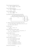
The resulting per-unit, per-phase equivalent circuit is shown below:
+
-
1∠0°
T
1
T
2
Line
L
1
L
2
0.010 j0.040 0.00723 j0.0482 0.040 j0.170
1.513
j1.134
-j3.36
(b) With the switch opened, the equivalent impedance of this circuit is
EQ
0.010 0.040 0.00723 0.0482 0.040 0.170 1.513 1.134Zj j j j=+ + + ++ ++
EQ
1.5702 1.3922 2.099 41.6Zj=+ =∠°
The resulting current is
10
0.4765 41.6
2.099 41.6
∠°
==∠−°
∠°
I
The load voltage under these conditions would be
()()
Load,pu Load
0.4765 41.6 1.513 1.134 0.901 4.7Zj== ∠−°+ =∠−°VI
()( )
Load Load,pu base3
0.901 480 V 432 VVVV== =
The power supplied to the load is
()()
2
2
Load,pu Load
0.4765 1.513 0.344PIR== =
()( )
Load Load,pu base
0.344 1000 kVA 344 kWPPS== =
The power supplied by the generator is
()( )
,pu
cos 1 0.4765 cos41.6 0.356
G
PVI
θ
== °=
()( )
,pu
sin 1 0.4765 sin 41.6 0.316
G
QVI
θ
== °=
()( )
,pu
1 0.4765 0.4765
G
SVI== =
()( )
,pu base
0.356 1000 kVA 356 kW
GG
PPS== =
()( )
,pu base
0.316 1000 kVA 316 kVAR
GG
QQS== =
()( )
,pu base
0.4765 1000 kVA 476.5 kVA
GG
SSS== =
The power factor of the generator is
62
PF cos 41.6 0.748 lagging=°=
(c) With the switch closed, the equivalent impedance of this circuit is
()()
()()
EQ
1.513 1.134 3.36
0.010 0.040 0.00723 0.0482 0.040 0.170
1.513 1.134 3.36
jj
Zj j j
jj
+−
=+ + + ++ +
++−
EQ
0.010 0.040 0.00788 0.0525 0.040 0.170 (2.358 0.109)Zj j j j=+++++++
EQ
2.415 0.367 2.443 8.65Zj=+ =∠°
The resulting current is
10
0.409 8.65
2.443 8.65
∠°
==∠−°
∠°
I
The load voltage under these conditions would be
()()
Load,pu Load
0.409 8.65 2.358 0.109 0.966 6.0Zj==∠−°+ =∠−°VI
()( )
Load Load,pu base3
0.966 480 V 464 VVVV== =
The power supplied to the two loads is the power supplied to the resistive component of the parallel
combination of the two loads: 2.358 pu.
()()
2
2
Load,pu Load
0.409 2.358 0.394PIR== =
()( )
Load Load,pu base
0.394 1000 kVA 394 kWPPS== =
The power supplied by the generator is
()( )
,pu
cos 1 0.409 cos6.0 0.407
G
PVI
θ
== °=
()( )
,pu
sin 1 0.409 sin 6.0 0.0428
G
QVI
θ
== °=
()( )
,pu
1 0.409 0.409
G
SVI== =
()( )
,pu base
0.407 1000 kVA 407 kW
GG
PPS== =
()( )
,pu base
0.0428 1000 kVA 42.8 kVAR
GG
QQS== =
()( )
,pu base
0.409 1000 kVA 409 kVA
GG
SSS== =
The power factor of the generator is
PF cos 6.0 0.995 lagging=°=
(d) The transmission losses with the switch open are:
()( )
2
2
line,pu line
0.4765 0.00723 0.00164PIR== =
()( )
line l ,pu base
0.00164 1000 kVA 1.64 kW
ine
PPS== =
The transmission losses with the switch closed are:
()( )
2
2
line,pu line
0.409 0.00723 0.00121PIR== =
()( )
line l ,pu base
0.00121 1000 kVA 1.21 kW
ine
PPS== =
Load 2 improved the power factor of the system, increasing the load voltage and the total power supplied to
the loads, while simultaneously decreasing the current in the transmission line and the transmission line
losses. This problem is a good example of the advantages of power factor correction in power systems.
63
Chapter 3:
Introduction to Power Electronics
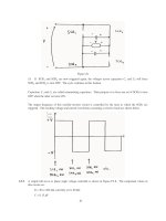
3-1. Calculate the ripple factor of a three-phase half-wave rectifier circuit, both analytically and using
MATLAB.
S
OLUTION
A three-phase half-wave rectifier and its output voltage are shown below
π
/6
5
π
/6
2
π
/3
()
sin
AM
vt V t
ω
=
() ( )
sin 2 / 3
BM
vt V t
ωπ
=−
() ( )
sin 2 /3
CM
vt V t
ωπ
=+
S
OLUTION
If we find the average and rms values over the interval from
π
/6 to 5
π
/6 (one period), these
values will be the same as the average and rms values of the entire waveform, and they can be used to
calculate the ripple factor. The average voltage is
()
5/6
/6
13
() sin
2
DC M
VvtdtVtdt
T
π
π
ωω
π
==
5
6
6
333333
cos 0.8270
22222
MM
DC MM
VV
Vt VV
π
π
ω
ππ π
=− =− − − = =
The rms voltage is
()
5/6
222
rms
/6
13
() sin
2
M
VvtdtVtdt
T
π
π
ωω
π
==
5/6
2
rms
/
6
311
sin 2
22 4
M
V
Vtt
π
π
ωω
π
=−
64
2
rms
315 15
sin sin
22664 3 3
M
V
V
ππ π π
π
=−−−
22
rms
315 3133
sin sin
234 3 3 23422
MM
VV
V
πππ π
ππ
=−−=−−−
22
rms
31333 3
0.8407
23422 234
MM
M
VV
VV
ππ
ππ
=−−−=+=
The resulting ripple factor is
22
rms
DC
0.8407
1 100% 1 100% 18.3%
0.8270
M
M
VV
r
VV
=−×= −×=
The ripple can be calculated with MATLAB using the
ripple
function developed in the text. We must
right a new function
halfwave3
to simulate the output of a three-phase half-wave rectifier. This output
is just the largest voltage of
()
tv
A
,
()
tv
B
, and
()
tv
C
at any particular time. The function is shown below:
function volts = halfwave3(wt)
% Function to simulate the output of a three-phase
% half-wave rectifier.
% wt = Phase in radians (=omega x time)
% Convert input to the range 0 <= wt < 2*pi
while wt >= 2*pi
wt = wt - 2*pi;
end
while wt < 0
wt = wt + 2*pi;
end
% Simulate the output of the rectifier.
a = sin(wt);
b = sin(wt - 2*pi/3);
c = sin(wt + 2*pi/3);
volts = max( [ a b c ] );
The function
ripple
is reproduced below. It is identical to the one in the textbook.
function r = ripple(waveform)
% Function to calculate the ripple on an input waveform.
% Calculate the average value of the waveform
nvals = size(waveform,2);
temp = 0;
for ii = 1:nvals
temp = temp + waveform(ii);
end
average = temp/nvals;
% Calculate rms value of waveform
65
temp = 0;
for ii = 1:nvals
temp = temp + waveform(ii)^2;
end
rms = sqrt(temp/nvals);
% Calculate ripple factor
r = sqrt((rms / average)^2 - 1) * 100;
Finally, the test driver program is shown below.
% M-file:
test_halfwave3.m
% M-file to calculate the ripple on the output of a
% three phase half-wave rectifier.
% First, generate the output of a three-phase half-wave
% rectifier
waveform = zeros(1,128);
for ii = 1:128
waveform(ii) = half wave3(ii*pi/64);
end
% Now calculate the ripple factor
r = ripple(waveform);
% Print out the result
string = ['The ripple is ' num2str(r) '%.'];
disp(string);
When this program is executed, the results are
»
test_halfwave3
The ripple is 18.2759%.
This answer agrees with the analytical solution above.
3-2. Calculate the ripple factor of a three-phase full-wave rectifier circuit, both analytically and using
MATLAB.
S
OLUTION
A three-phase half-wave rectifier and its output voltage are shown below
66
T
/12
()
sin
AM
vt V t
ω
=
() ( )
sin 2 / 3
BM
vt V t
ωπ
=−
() ( )
sin 2 /3
CM
vt V t
ωπ
=+
S
OLUTION
By symmetry, the rms voltage over the interval from 0 to T/12 will be the same as the rms
voltage over the whole interval. Over that interval, the output voltage is:
() () ()
22
sin sin
33
CB M M
vt vt vt V t V t
ππ
ωω
=−= +− −
()
22 22
sin cos cos sin sin cos cos sin
33 33
MM
vt V t t V t t
ππ ππ
ωω ωω
=+−−
()
2
2cos sin 3cos
3
M
vt V t t
π
ωω
==
Note that the period of the waveform is
2/T
πω
=
, so T/12 is
/
6
πω
. The average voltage over the
interval from 0 to T/12 is
/6
/
6
0
0
16 63
() 3 cos sin
DC M M
Vvtdt VtdtVt
T
πω
πω
ω
ωω
ππ
== =
33
1.6540
DC M M
VV V
π
==
The rms voltage is
/6
222
rms
0
16
() 3 cos
M
Vvtdt Vtdt
T
πω
ω
ω
π
==
67
/
6
2
rms
0
18 1 1
sin 2
24
M
VVt t
πω
ω
ω
πω
=+
rms
18 1 3 9 3
sin 1.6554
12 4 3 2 4
MMM
VV V V
ωπ π
πωω π
=+=+=
The resulting ripple factor is
2
2
rms
DC
1.6554
1 100% 1 100% 4.2%
1.6540
M
M
VV
r
VV
=−×= −×=
The ripple can be calculated with MATLAB using the
ripple function developed in the text. We must
right a new function
fullwave3
to simulate the output of a three-phase half-wave rectifier. This output
is just the largest voltage of
()
tv
A
,
()
tv
B
, and
()
tv
C
at any particular time. The function is shown below:
function volts = fullwave3(wt)
% Function to simulate the output of a three-phase
% full-wave rectifier.
% wt = Phase in radians (=omega x time)
% Convert input to the range 0 <= wt < 2*pi
while wt >= 2*pi
wt = wt - 2*pi;
end
while wt < 0
wt = wt + 2*pi;
end
% Simulate the output of the rectifier.
a = sin(wt);
b = sin(wt - 2*pi/3);
c = sin(wt + 2*pi/3);
volts = max( [ a b c ] ) - min( [ a b c ] );
The test driver program is shown below.
% M-file: test_fullwave3.m
% M-file to calculate the ripple on the output of a
% three phase full-wave rectifier.
% First, generate the output of a three-phase full-wave
% rectifier
waveform = zeros(1,128);
for ii = 1:128
waveform(ii) = fullwave3(ii*pi/64);
end
% Now calculate the ripple factor
r = ripple(waveform);
% Print out the result
string = ['The ripple is ' num2str(r) '%.'];
disp(string);
68
When this program is executed, the results are
» test_fullwave3
The ripple is 4.2017%.
This answer agrees with the analytical solution above.
3-3. Explain the operation of the circuit shown in Figure P3-1. What would happen in this circuit if switch S
1
were closed?
S
OLUTION
Diode D
1
and D
2
together with the transformer form a full-wave rectifier. Therefore, a voltage
oriented positive-to-negative as shown will be applied to the SCR and the control circuit on each half cycle.
(1) Initially, the SCR is an open circuit, since v
1
< V
BO
for the SCR. Therefore, no current flows to the
load and v
LOAD
= 0.
(2) Voltage v
1
is applied to the control circuit, charging capacitor C
1
with time constant RC
1
.
(3) When v
C
> V
BO
for the DIAC, it conducts, supplying a gate current to the SCR.
(4) The gate current in the SCR lowers its breakover voltage, and the SCR fires. When the SCR fires,
current flows through the SCR and the load.
(5) The current flow continues until i
D
falls below I
H
for the SCR (at the end of the half cycle). The
process starts over in the next half cycle.
69
If switch S
1
is shut, the charging time constant is increased, and the DIAC fires later in each half cycle.
Therefore, less power is supplied to the load.
3-4. What would the rms voltage on the load in the circuit in Figure P3-1 be if the firing angle of the SCR were
(a) 0°, (b) 30°, (c) 90°?
S
OLUTION
The input voltage to the circuit of Figure P3-1 is
()
ttv
ω
sin339
ac
=
, where
rad/s 377=
ω
Therefore, the voltage on the secondary of the transformer will be
()
ttv
ω
sin5.169
ac
=
(a) The average voltage applied to the load will be the integral over the conducting portion of the half
cycle divided by
π
/
ω
, the period of a half cycle. For a firing angle of 0°, the average voltage will be
/
/
ave
0
00
11
() sin cos
T
MM
VvtdtVtdtVt
T
πω
πω
ω
ωω
ππ
== =−
[]
()( )
ave
12
1 1 0.637 169.5 V 108 V
MM
VV V
ππ
=− − − = = =
(b) For a firing angle of 30°, the average voltage will be
/
/
ave
/
6
/6 /6
11
() sin cos
T
MM
VvtdtVtdtVt
T
πω
πω
π
ππ
ω
ωω
ππ
== =−
()( )
ave
1323
1 0.594 169.5 V 101 V
22
MM
VV V
ππ
+
=− − − = = =
(c) For a firing angle of 90°, the average voltage will be
/
/
ave
/
2
/2 /2
11
() sin cos
T
MM
VvtdtVtdtVt
T
πω
πω
π
ππ
ω
ωω
ππ
== =−
70
[]
()( )
ave
11
1 0.318 169.5 V 54 V
MM
VV V
ππ
=− − = = =
3-5. For the circuit in Figure P3-1, assume that
V
BO
for the DIAC is 30 V, C
1
is 1 µF, R is adjustable in the
range 1-20 kΩ, and that switch S
1
is open. What is the firing angle of the circuit when R is 10 kΩ? What
is the rms voltage on the load under these conditions?
Note:
Problem 3-5 is significantly harder for many students, since it involves solving
a differential equation with a forcing function. This problem should only be
assigned if the class has the mathematical sophistication to handle it.
S
OLUTION
At the beginning of each half cycle, the voltages across the DIAC and the SCR will both be
smaller then their respective breakover voltages, so no current will flow to the load (except for the very tiny
current charging capacitor C), and v
load
(t) will be 0 volts. However, capacitor C charges up through
resistor R, and when the voltage v
C
(t) builds up to the breakover voltage of D
1
, the DIAC will start to
conduct. This current flows through the gate of SCR
1
, turning the SCR ON. When it turns ON, the
voltage across the SCR will drop to 0, and the full source voltage v
S
(t) will be applied to the load,
producing a current flow through the load. The SCR continues to conduct until the current through it falls
below I
H
, which happens at the very end of the half cycle.
Note that after D
1
turns on, capacitor C discharges through it and the gate of the SCR. At the end of the
half cycle, the voltage on the capacitor is again essentially 0 volts, and the whole process is ready to start
over again at the beginning of the next half cycle.
To determine when the DIAC and the SCR fire in this circuit, we must determine when v
C
(t) exceeds V
BO
for D
1
. This calculation is much harder than in the examples in the book, because in the previous problems
the source was a simple DC voltage source, while here the voltage source is sinusoidal. However, the
principles are identical.
(a) To determine when the SCR will turn ON, we must calculate the voltage v
C
(t), and then solve for the time
at which v
C
(t) exceeds V
BO
for D
1
. At the beginning of the half cycle, D
1
and SCR
1
are OFF, and the
voltage across the load is essentially 0, so the entire source voltage v
S
(t) is applied to the series RC circuit.
To determine the voltage v
C
(t) on the capacitor, we can write a Kirchhoff's Current Law equation at the
node above the capacitor and solve the resulting equation for v
C
(t).
0
21
=+ ii
(since the DIAC is an open circuit at this time)
0
1
=+
−
C
C
v
dt
d
C
R
vv
71
1
11
v
RC
v
RC
v
dt
d
CC
=+
t
R
C
V
v
R
C
v
dt
d
M
CC
ω
sin
1
=+
The solution can be divided into two parts, a natural response and a forced response. The natural response
is the solution to the differential equation
1
0
CC
d
vv
dt RC
+=
The solution to the natural response differential equation is
()
,
e
t
RC
Cn
vtA
−
=
where the constant A must be determined from the initial conditions in the system. The forced response is
the steady-state solution to the equation
1
sin
M
CC
dV
vv t
dt RC RC
ω
+=
It must have a form similar to the forcing function, so the solution will be of the form
(
)
,1 2
sin cos
Cf
vtB tB t
ωω
=+
where the constants
1
B and
2
B must be determined by substitution into the original equation. Solving for
1
B and
2
B yields:
()()
12 12
1
sin cos sin cos sin
M
dV
BtBt BtBt t
dt RC RC
ωω ωω ω
++ +=
()()
12 12
1
cos in sin cos sin
M
V
BtBst B tB t t
RC RC
ωωω ω ω ω ω
−+ +=
cosine equation:
12
1
0
BB
RC
ω
+=
⇒
21
BRCB
ω
=−
sine equation:
21
1
M
V
BB
RC RC
ω
−+ =
2
11
1
M
V
RC B B
RC RC
ω
+=
2
1
1
M
V
RC B
RC RC
ω
+=
222
1
1
M
RC V
B
RC RC
ω
+
=
Finally,
72
1
222
1
M
V
B
RC
ω
=
+
and
2
222
1
M
RC V
B
RC
ω
ω
−
=
+
Therefore, the forced solution to the equation is
()
,
222 222
sin cos
11
MM
Cf
VRCV
vt t t
RC RC
ω
ωω
ωω
=−
++
and the total solution is
(
)
(
)
(
)
,,CCnCf
vt v t v t=+
()
222 222
sin cos
11
t
MM
RC
C
VRCV
vt Ae t t
RC RC
ω
ωω
ωω
−
=+ −
++
The initial condition for this problem is that the voltage on the capacitor is zero at the beginning of the half-
cycle:
()
0
222 222
0 sin 0 cos 00
11
MM
RC
C
VRCV
vAe
RC RC
ω
ωω
−
=+ − =
++
222
0
1
M
RC V
A
RC
ω
ω
−=
+
222
1
M
RC V
A
RC
ω
ω
=
+
Therefore, the voltage across the capacitor as a function of time before the DIAC fires is
()
222 222 222
sin cos
11 1
t
MM M
RC
C
RC V V RC V
vt e t t
RC RC RC
ωω
ωω
ωω ω
−
=+ −
++ +
If we substitute the known values for R, C,
ω
, and V
M
, this equation becomes
(
)
100
42 11.14 sin 42 cos
t
C
vt e t t
ωω
−
=+ −
This equation is plotted below:
It reaches a voltage of 30 V at a time of 3.50 ms. Since the frequency of the waveform is 60 Hz, the
waveform there are 360
°
in 1/60 s, and the firing angle
α
is
73
()
360
3.50 ms 75.6
1/60 s
α
°
==°
or 1.319 radians
Note: This problem could also have been solved using Laplace Transforms, if desired.
(b) The rms voltage applied to the load is
/
222
rms
1
() sin
M
VvtdtVtdt
T
πω
α
ω
ω
π
==
/
2
rms
11
sin 2
24
M
V
Vtt
πω
α
ωω
π
=−
()()
2
rms
11
sin 2 sin2
24
M
V
V
πα π α
π
=−−−
rms
0.3284 0.573 97.1 V
MM
VV V===
3-6. One problem with the circuit shown in Figure P3-1 is that it is very sensitive to variations in the input
voltage
vt
ac
(). For example, suppose the peak value of the input voltage were to decrease. Then the time
that it takes capacitor C
1
to charge up to the breakover voltage of the DIAC will increase, and the SCR will
be triggered later in each half cycle. Therefore, the rms voltage supplied to the load will be reduced both by
the lower peak voltage and by the later firing. This same effect happens in the opposite direction if
vt
ac
()
increases. How could this circuit be modified to reduce its sensitivity to variations in input voltage?
S
OLUTION
If the voltage charging the capacitor could be made constant or nearly so, then the feedback
effect would be stopped and the circuit would be less sensitive to voltage variations. A common way to do
this is to use a zener diode that fires at a voltage greater than
BO
V for the DIAC across the RC charging
circuit. This diode holds the voltage across the RC circuit constant, so that the capacitor charging time is
not much affected by changes in the power supply voltage.
v
C
R
74
3-7. Explain the operation of the circuit shown in Figure P3-2, and sketch the output voltage from the circuit.
S
OLUTION
This circuit is a single-phase voltage source inverter.
(1) Initially, suppose that both SCRs are OFF. Then the voltage on the transformer T
3
will be 0, and
voltage V
DC
will be dropped across SCR
1
and SCR
2
as shown.
(2) Now, apply a pulse to transformer T
1
that turns on SCR
1
. When that happens, the circuit looks like:
Since the top of the transformer is now grounded, a voltage V
DC
appears across the upper winding as
shown. This voltage induces a corresponding voltage on the lower half of the winding, charging capacitor
C
1
up to a voltage of 2V
DC
, as shown.
Now, suppose that a pulse is applied to transformer T
2
. When that occurs, SCR
2
becomes a short circuit,
and SCR
1
is turned OFF by the reverse voltage applied to it by capacitor C
1
(forced commutation). At that
time, the circuit looks like:
Now the voltages on the transformer are reversed, charging capacitor C
1
up to a voltage of 2V
DC
in the
opposite direction. When SCR
1
is triggered again, the voltage on C
1
will turn SCR
2
OFF.
The output voltage from this circuit would be roughly a square wave, except that capacitor C
2
filters it
somewhat.
75
(
Note: The above discussion assumes that transformer T
3
is never in either state long enough for it to
saturate.)
3-8. Figure P3-3 shows a relaxation oscillator with the following parameters:
R
1
= variable
Ω= 1500
2
R
1.0 FC
µ
=
V 100
DC
=V
BO
30 VV = 0.5 mA
H
I =
(a) Sketch the voltages
vt
C
(), vt
D
(), and vt
o
() for this circuit.
(b) If R
1
is currently set to 500 k
Ω
, calculate the period of this relaxation oscillator.
S
OLUTION
(a) The voltages v
C
(t), v
D
(t) and v
o
(t) are shown below. Note that v
C
(t) and v
D
(t) look the same during
the rising portion of the cycle. After the PNPN Diode triggers, the voltage across the capacitor decays with
time constant
τ
2
=
R
1
R
2
R
1
+ R
2
C, while the voltage across the diode drops immediately.
76
(b) When voltage is first applied to the circuit, the capacitor C charges with a time constant
τ
1
= R
1
C =
(500 kΩ)(1.00 µF) = 0.50 s. The equation for the voltage on the capacitor as a function of time during the
charging portion of the cycle is
()
1
t
RC
C
vt ABe
−
=+
where A and B are constants depending upon the initial conditions in the circuit. Since v
C
(0) = 0 V and
v
C
(
∞
) = 100 V, it is possible to solve for A and B.
A = v
C
(∞) = 100 V
A + B = v
C
(0) = 0 V
⇒
B = -100 V
Therefore,
()
0.50
100 100 V
t
C
vt e
−
=−
The time at which the capacitor will reach breakover voltage is found by setting v
C
(t) = V
BO
and solving for
time t
1
:
77
1
100 V 30 V
0.50 ln 178 ms
100 V
t
−
=− =
Once the PNPN Diode fires, the capacitor discharges through the parallel combination of R
1
and R
2
, so the
time constant for the discharge is
(
)
(
)
()
12
2
12
500 k 1.5 k
1.0 F 0.0015 s
500 k 1.5 k
RR
C
RR
τµ
ΩΩ
== =
+Ω+Ω
The equation for the voltage on the capacitor during the discharge portion of the cycle is
()
2
t
C
vt ABe
τ
−
=+
()
2
BO
t
C
vt V e
τ
−
=
The current through the PNPN diode is given by
()
2
BO
2
t
D
V
it e
R
τ
−
=
If we ignore the continuing trickle of current from R
1
, the time at which i
D
(t) reaches I
H
is
()
(
)
(
)
2
22
BO
0.0005 A 1500
ln 0.0015 ln 5.5 ms
30 V
H
IR
tRC
V
Ω
=− =− =
Therefore, the period of the relaxation oscillator is T = 178 ms + 5.5 ms = 183.5 ms, and the frequency of
the relaxation oscillator is f = 1/T = 5.45 Hz.
3-9. In the circuit in Figure P3-4, T
1
is an autotransformer with the tap exactly in the center of its winding.
Explain the operation of this circuit. Assuming that the load is inductive, sketch the voltage and current
applied to the load. What is the purpose of
SCR
2
? What is the purpose of D
2
? (This chopper circuit
arrangement is known as a Jones circuit.)
S
OLUTION
First, assume that SCR
1
is triggered. When that happens, current will flow from the power
supply through SCR
1
and the bottom portion of transformer T
1
to the load. At that time, a voltage will be
applied to the bottom part of the transformer which is positive at the top of the winding with respect to the
bottom of the winding. This voltage will induce an equal voltage in the upper part of the autotransformer
78
winding, forward biasing diode D
1
and causing the current to flow up through capacitor C. This current
causes C to be charged with a voltage that is positive at its bottom with respect to its top. (This condition
is shown in the figure above.)
Now, assume that SCR
2
is triggered. When SCR
2
turns ON, capacitor C applies a reverse-biased voltage
to SCR
1
, shutting it off. Current then flow through the capacitor, SCR
2
, and the load as shown below.
This current charges C with a voltage of the opposite polarity, as shown.
SCR
2
will cut off when the capacitor is fully charged. Alternately, it will be cut off by the voltage across
the capacitor if SCR
1
is triggered before it would otherwise cut off.
In this circuit, SCR
1
controls the power supplied to the load, while SCR
2
controls when SCR
1
will be
turned off. Diode D
2
in this circuit is a free-wheeling diode, which allows the current in the load to
continue flowing for a short time after SCR
1
turns off.
79
3-10. A series-capacitor forced commutation chopper circuit supplying a purely resistive load is shown in Figure
P3-5.
DC
120 VV = 20 kR =Ω
8 mA
H
I =
2
LOAD
250 R =Ω
BO
200 VV =
150 FC
µ
=
(a) When
SCR
1
is turned on, how long will it remain on? What causes it to turn off?
(b) When
SCR
1
turns off, how long will it be until the SCR can be turned on again? (Assume that three
time constants must pass before the capacitor is discharged.)
(c) What problem or problems do these calculations reveal about this simple series-capacitor forced
commutation chopper circuit?
(d) How can the problem(s) described in part (c) be eliminated?
Solution
(a) When the SCR is turned on, it will remain on until the current flowing through it drops below I
H
.
This happens when the capacitor charges up to a high enough voltage to decrease the current below I
H
. If
we ignore resistor R (because it is so much larger than R
LOAD
), the capacitor charges through resistor
R
LOAD
with a time constant
τ
LOAD
= R
LOAD
C = (250
Ω
)(150
µ
F) = 0.0375 s. The equation for the voltage
on the capacitor as a function of time during the charging portion of the cycle is
()
LOAD
t
RC
C
vt ABe
−
=+
where A and B are constants depending upon the initial conditions in the circuit. Since v
C
(0) = 0 V and
v
C
(
∞
) = V
DC
, it is possible to solve for A and B.
A = v
C
(∞) = V
DC
A + B = v
C
(0) = V
DC
⇒
B = -V
DC
Therefore,
2
The first printing of this book incorrectly stated that I
H
is 6 mA.
80
()
LOAD
DC DC
V
t
RC
C
vt V V e
−
=−
The current through the capacitor is
() ()
CC
d
it C vt
dt
=
()
LOAD
DC DC
t
RC
C
d
it C V V e
dt
−
=−
()
LOAD
DC
LOAD
A
t
RC
C
V
it e
R
−
=
Solving for time yields
(
)
(
)
22
LOAD
DC DC
ln 0.0375 ln
CC
itR itR
tRC
VV
=− =−
The current through the SCR consists of the current through resistor R plus the current through the
capacitor. The current through resistor R is 120 V / 20 k
Ω
= 6 mA, and the holding current of the SCR is
8 mA, so the SCR will turn off when the current through the capacitor drops to 2 mA. This occurs at time
(
)
(
)
2 mA 250
0.0375 ln 0.206 s
120 V
t
Ω
=− =
(b) The SCR can be turned on again once the capacitor has discharged. The capacitor discharges
through resistor R. It can be considered to be completely discharged after three time constants. Since
τ
=
RC = (20 k
Ω
)(150
µ
F) = 3 s, the SCR will be ready to fire again after 9 s.
(c) In this circuit, the ON time of the SCR is much shorter than the reset time for the SCR, so power can
flow to the load only a very small fraction of the time. (This effect would be less exaggerated if the ratio of
R to R
LOAD
were smaller.)
(d) This problem can be eliminated by using one of the more complex series commutation circuits
described in Section 3-5. These more complex circuits provide special paths to quickly discharge the
capacitor so that the circuit can be fired again soon.
3-11. A parallel-capacitor forced commutation chopper circuit supplying a purely resistive load is shown in
Figure P3-6.
DC
120 VV =
1
20 kR =Ω
5 mA
H
I =
load
250 R =Ω
81
BO
250 VV = 15 FC
µ
=
(a) When
SCR
1
is turned on, how long will it remain on? What causes it to turn off?
(b) What is the earliest time that
SCR
1
can be turned off after it is turned on? (Assume that three time
constants must pass before the capacitor is charged.)
(c) When
SCR
1
turns off, how long will it be until the SCR can be turned on again?
(d) What problem or problems do these calculations reveal about this simple parallel-capacitor forced
commutation chopper circuit?
(e) How can the problem(s) describe in part (d) be eliminated?
S
OLUTION
(a) When SCR
1
is turned on, it will remain on indefinitely until it is forced to turn off. When SCR
1
is turned
on, capacitor C charges up to V
DC
volts with the polarity shown in the figure above. Once it is charged,
SCR
1
can be turned off at any time by triggering SCR
2
. When SCR
2
is triggered, the voltage across it
drops instantaneously to about 0 V, which forces the voltage at the anode of SCR
1
to be -V
DC
volts, turning
SCR
1
off. (Note that SCR2 will spontaneously turn off after the capacitor discharges, since V
DC
/ R
1
< I
H
for SCR
2
.)
(b) If we assume that the capacitor must be fully charged before SCR
1
can be forced to turn off, then the time
required would be the time to charge the capacitor. The capacitor charges through resistor R
1
, and the time
constant for the charging is
τ
= R
1
C = (20 k
Ω
)(15
µ
F) = 0.3 s. If we assume that it takes 3 time constants
to fully charge the capacitor, then the time until SCR
1
can be turned off is 0.9 s.
(Note that this is not a very realistic assumption. In real life, it is possible to turn off SCR
1
with less than a
full V
DC
volts across the capacitor.)
(c) SCR
1
can be turned on again after the capacitor charges up and SCR
2
turns off. The capacitor charges
through R
LOAD
, so the time constant for charging is
τ
= R
LOAD
C = (250
Ω
)(15
µ
F) = 0.00375 s
and SCR
2
will turn off in a few milliseconds.
(d) In this circuit, once SCR
1
fires, a substantial period of time must pass before the power to the load can be
turned off. If the power to the load must be turned on and off rapidly, this circuit could not do the job.
82
(e) This problem can be eliminated by using one of the more complex parallel commutation circuits described
in Section 3-5. These more complex circuits provide special paths to quickly charge the capacitor so that
the circuit can be turned off quickly after it is turned on.
3-12. Figure P3-7 shows a single-phase rectifier-inverter circuit. Explain how this circuit functions. What are
the purposes of C
1
and C
2
? What controls the output frequency of the inverter?
S
OLUTION
The last element in the filter of this rectifier circuit is an inductor, which keeps the current flow
out of the rectifier almost constant. Therefore, this circuit is a current source inverter. The rectifier and
filter together produce an approximately constant dc voltage and current across the two SCRs and diodes at
the right of the figure. The applied voltage is positive at the top of the figure with respect to the bottom of
the figure. To understand the behavior of the inverter portion of this circuit, we will step through its
operation.
(1) First, assume that SCR
1
and SCR
4
are triggered. Then the voltage V will appear across the load
positive-to-negative as shown in Figure (a). At the same time, capacitor C
1
will charge to V volts through
diode D
3
, and capacitor C
2
will charge to V volts through diode D
2
.
(a)
(2) Now, assume that SCR
2
and SCR
3
are triggered. At the instant they are triggered, the voltage across
capacitors C
1
and C
2
will reverse bias SCR
1
and SCR
4
, turning them OFF. Then a voltage of V volts will
appear across the load positive-to-negative as shown in Figure (b). At the same time, capacitor C
1
will
charge to V volts with the opposite polarity from before, and capacitor C
2
will charge to V volts with the
opposite polarity from before.