RECENT ADVANCES IN NANOFABRICATION TECHNIQUES AND APPLICATIONS_2 pot
Bạn đang xem bản rút gọn của tài liệu. Xem và tải ngay bản đầy đủ của tài liệu tại đây (23.96 MB, 264 trang )
Part 4
EUV Lithography and Resolution
Enhancement Techniques
18
Laser-Plasma Extreme Ultraviolet Source
Incorporating a Cryogenic Xe Target
Sho Amano
University of Hyogo
Laboratory of Advanced Science and Technology for Industry (LASTI)
Japan
1. Introduction
Optical lithography is a core technique used in the industrial mass production of
semiconductor memory chips. To increase the memory size per chip, shorter wavelength
light is required for the light source. ArF excimer laser light (193 nm) is used at present and
extreme ultraviolet (EUV) light (13.5 nm) is proposed in next-generation optical lithography.
There is currently worldwide research and development for lithography using EUV light
(Bakshi, 2005). EUV lithography (EUVL) was first demonstrated by Kinoshita et al. in 1984
at NTT, Japan (Kinoshita et al., 1989). He joined our laboratory in 1995 and has since been
actively developing EUVL technology using our synchrotron facility NewSUBARU. Today,
EUVL is one of the major themes studied at our laboratory.
To use EUVL in industry, however, a small and strong light source instead of a synchrotron
is required. Our group began developing laser-produced plasma (LPP) sources for EUVL in
the mid-1990s (Amano et al., 1997). LPP radiation from high-density, high-temperature
plasma, which is achieved by illuminating a target with high-peak-power laser irradiation,
constitutes an attractive, high-brightness point source for producing radiation from EUV
light to x-rays.
Light at a wavelength of 13.5 nm with 2% bandwidth is required for the EUV light source,
which is limited by the reflectivity of Mo/Si mirrors in a projection lithography system. Xe
and Sn are known well as plasma targets with strong emission around 13.5 nm. Xe was
mainly studied initially because of the debris problem, in which debris emitted from plasma
with EUV light damages mirrors near the plasma, quickly degrading their reflectivity. This
problem was of particular concern in the case of a metal target such as Sn because the metal
would deposit and remain on the mirrors. On the other hand, Xe is an inert gas and does not
deposit on mirrors, and thus has been studied as a deposition-free target. Because of this
advantage, researchers initially studied Xe. To provide a continuous supply of Xe at the
laser focal point, several possible approaches have been investigated: employing a Xe gas
puff target (Fiedrowicz et al., 1999), Xe cluster jet (Kubiak et al., 1996), Xe liquid jet
(Anderson et al., 2004; Hansson et al., 2004), Xe capillary jet (Inoue et al., 2007), stream of
liquid Xe droplets (Soumagne et al., 2005), and solid Xe pellets (Kubiak et al., 1995). Here,
there are solid and liquid states, and their cryogenic Xe targets were expected to provide
higher laser-to-EUV power conversion efficiency (CE) owing to their higher density
compared with the gas state. In addition, a smaller gas load to be evacuated by the exhaust
pump system was expected.
Recent Advances in Nanofabrication Techniques and Applications
354
We have also studied a cryogenic Xe solid target. In that study, we measured the EUV
emission spectrum in detail, and we found and first reported that the emission peak of Xe
was at 10.8 nm, not 13 nm (Shimoura et al., 1998). This meant we could only use the tail of
the Xe plasma emission spectrum, not its peak, as the radiation at 13.5 nm wavelength with
2% bandwidth. From this, improvements in the CE at 13.5 nm with 2% bandwidth became a
most critical issue for the Xe plasma source; such improvements were necessary to reduce
the pumped laser power and cost of the whole EUV light source. On the other hand, the
emission peak of a Sn target is at 13.5 nm; therefore, Sn intrinsically has a high CE at 13.5 nm
with 2% bandwidth. The CE for Sn is thus higher than that for Xe at present, in spite of our
efforts to improve the CE for Xe. This resulted in a trend of using Sn rather than Xe in spite
of the debris problem. Today, Cymer (Brandt et al., 2010) and Gigaphoton (Mizoguti et al.,
2010), the world’s leading manufacturers of LPP-EUV sources, are developing sources using
Sn targets pumped with CO
2
lasers while making efforts to mitigate the effects of debris.
In the historical background mentioned above, we developed an LPP-EUV source composed
of 1) a fast-rotating cryogenic drum system that can continuously supply a solid Xe target
and 2) a high-repetition-rate pulse Nd:YAG slab laser. We have developed the source in
terms of its engineering and investigated potential improvements in the CE at 13.5 nm with
2% bandwidth. The CE depends on spatial and temporal Xe plasma conditions (e.g., density,
temperature, and size). To achieve a high CE, we controlled the condition parameters and
attempted to optimize them by changing the pumping laser conditions. We initially focused
on parameters at the wavelength of 13.5 nm with 2% bandwidth required for an EUV
lithography source, but the original emission from the Xe plasma has a broad spectrum at 5–
17 nm. We noted that this broad source would be highly efficient and very useful for many
other applications, if not limiting for EUVL. Therefore, we estimated our source in the
wavelength of 5–17 nm. Though Xe is a deposition-free target, there may be sputtering due
to the plasma debris. We therefore investigated the plasma debris emitted from our LPP
source, which consists of fast ions, fast neutrals, and ice fragments. To mitigate the
sputtering, we are investigating the use of Ar buffer gas. In this chapter, we report on the
status of our LPP-EUV source and discuss its possibilities.
2. Target system – Rotating cryogenic drum
We considered using a cryogenic solid state Xe target and developed a rotating drum
system to supply it continuously, as shown in Fig. 1
(Fukugaki et al., 2006). A cylindrical
drum is filled with liquid nitrogen, and the copper surface is thereby cooled to the
temperature of liquid nitrogen. Xe gas blown onto the surface condenses to form a solid Xe
layer. The drum coated with a solid Xe layer rotates around the vertical z-axis and moves up
and down along the z-axis during rotation, moving spirally so that a fresh target surface is
supplied continuously for every laser shot. A container wall surrounds the drum surface,
except for an area around the laser focus point. This maintains a relatively high-density Xe
gas in the gap between the container wall and the drum surface so as to achieve a high
growth rate of the layer and fast recovery of the laser craters during rotation. The container
wall also suppresses Xe gas leakage to the vacuum chamber to less than 5%, and the
vacuum pressure inside the chamber is kept at less than 0.5 Pa. The diameter of the drum is
10 cm. Its mechanical rotation and up–down speed are tunable at 0–1200 rpm and 0–10
mm/s in a range of 3 cm respectively.
Laser-Plasma Extreme Ultraviolet Source Incorporating a Cryogenic Xe Target
355
Fig. 1. Illustration of (a) the top view of the rotating cryogenic drum, (b) the side view, and
(c) the wiper.
First, we formed a solid Xe layer with thickness of 300–500 m on the drum surface and
measured the size of the laser crater, which depends on the laser pulse energy. The crater
diameter was measured directly from a microscope image, and its depth was roughly
estimated from the number of shots needed to burn through the known thickness of the
layer. A Q-switched 1064 nm Nd:YAG laser was focused on the Xe target surface with a spot
diameter of 90 m. Measured crater diameters D
c
and crater depths
c
are plotted in Fig. 2
for a laser energy range of 0.04–0.7 J. From the results in Fig. 2, a thickness of more than 200
m was found to be sufficient for a laser shot of 1 J not to damage the drum surface. We
then decided the target thickness to be 500 m.
Two wipers are mounted on the container wall as shown in Fig.1 (a) to adjust the thickness
of the solid Xe layer to 500 m. As shown in Fig. 1 (c), the V-figure wipers also collect the Xe
target powder on the craters produced by laser irradiation, thereby increasing the recovery
Recent Advances in Nanofabrication Techniques and Applications
356
speed. The wipers demonstrated a recovery speed of 150 m/s up to a rotation speed of
1000 rpm, at a Xe flow rate of 400 mL/min.
Fig. 2. Measured diameter and depth of a crater as a function of the irradiating laser
energy.
Next, operational parameters of the drum are discussed to achieve high-repetition-rate laser
pulse irradiation. In Fig. 1(b), R is the rotation speed, r is the radius of the drum, and L is the
range of motion (scanning width of the target) along the rotational axis (z-axis). When the
laser pulses are irradiated with frequency f, craters form on the target with separation length
d between adjacent craters. The recovery time of a crater is T. Under the condition that
craters do not overlap, f and T can be written as
2 rR
f
d
(1)
2
2 rL
T
fd
(2)
For example, if we assume laser energy of E
L
= 1 J, a formed crater has a diameter of D
c
=
300 m and a depth of
c
= 160 m, and d must be at least 300 m for the craters not to
overlap. At r = 5 cm and R = 1000 rpm, we obtain f = 17 kHz from Eq. (1). When f = 10 kHz
and L = 3 cm, T is calculated to be 10 s using Eq. (2), and we know that a recovery speed of
the crater (V
c
=
c
/T) of 16 m/s is required. Here, we have already obtained V
c
= 150 m/s
via the wiper effect and the required speed has been achieved.
Laser-Plasma Extreme Ultraviolet Source Incorporating a Cryogenic Xe Target
357
Although flaking of the target layer due to superimposition of shock and/or thermal waves
produced by continuous laser pulses was a concern for high-repetition pulse operation,
model experiments and calculations show that there is no problem up to 1 J per pulse and 10
kHz (Inoue et al., 2006).
From the above results, we conclude that the rotating drum system we developed can
supply the target continuously, achieving the required laser irradiation of 10 kHz and 1 J,
and thus realizing a high-average-power EUV light source.
3. Drive laser – Nd:YAG slab laser
High peak power and high focusability (i.e., high beam quality) are required for a driving
laser to produce plasma. In addition, high average power is required for high throughput in
industrial use such as EUVL. We express such a laser as a high average and high peak
brightness laser, for which the average brightness and peak brightness are defined as average
power/(·M
2
)
2
and peak power/(·M
2
)
2
, respectively; we began studying such lasers in the
1990s (Amano et al, 1997,1999).
We attempted to realize a high average and high peak brightness laser using a solid-state
Nd:YAG laser (Amano et al., 2001). The thermal-lens effect and thermally induced
birefringence in an active medium are serious for such a laser; thus, thermal management of
the amplifier head is more critical, and the design of the amplifier system must more
efficiently extract energy and more accurately correct the remaining thermally induced
wavefront aberrations in the pumping head. To meet these requirements, we developed a
phase-conjugated master-oscillator-power-amplifier (PC-MOPA) Nd:YAG laser system
consisting of a diode-pumped master oscillator and flash-lamp-pumped angular-
multiplexing slab power-amplifier geometry incorporating a stimulated-Brillouin-scattering
phase-conjugate mirror (SBS-PCM) and image relays (IR). The system design and a
photograph are shown in Fig. 3. This laser demonstrated simultaneous maximum average
power of 235 W and maximum peak power of 30 MW with M
2
= 1.5. The maximum pulse
energy was 0.73 J with pulse duration of 24 ns at a pulse repetition rate of 320 pps. We
therefore obtained, simultaneously, both high average brightness of 7 × 10
9
W/cm
2
·sr and
high peak brightness of 1 × 10
15
W/cm
2
·sr.
This peak brightness is enough to produce plasma but the average brightness needs to be
higher for EUVL applications. The maximum average power is mainly limited by the
thermal load caused by flash-lamp-pumping in amplifiers. The system design rules that we
confirmed predicted that average output power at the kilowatt level can be achieved by
replacing lamp pumping in the amplifier with laser-diode pumping. Since our work, it
seems that there has been no major progress in laser engineering for such high average and
high peak brightness lasers. Average power of more than 10 kW has been achieved in
continuous-wave solid-state lasers using configurations of fibers (ex. IPG Photonics Corp.)
or thin discs (ex. TRUMPF GmbH). On the other hand, for the short-pulse lasers mentioned
above, the maximum average power remains around 1 kW (Soumagne et al., 2005), which is
more than an order of magnitude less than the ~30 kW required for an industrial EUVL
source. This is one of the reasons why CO
2
lasers have been preferred over Nd:YAG lasers
as the driving laser. To further the industrial use of solid-state lasers, there needs to be a
breakthrough to increase the average power.
Recent Advances in Nanofabrication Techniques and Applications
358
Fig. 3. Experimental setup and photograph of the PC-MOPA laser system.
4. EUV source
Figure 4 is an illustration and a photograph of the LPP-EUV source composed of a rotating
cryogenic drum and Nd:YAG slab laser. The drum, detectors, and irradiating samples are
installed in a vacuum chamber because EUV light cannot transmit through air. Driving laser
pulses passing through the window are focused perpendicularly on the target by the lens so
that Xe plasma is produced and EUV radiation is emitted. At a repetition rate of 320 Hz and
average power of 110 W, the laser pulses irradiate the Xe solid target on the rotating drum
with laser intensity of ~10
10
W/cm
2
. The rotation speed is 130 rpm and the vertical speed 3
Laser-Plasma Extreme Ultraviolet Source Incorporating a Cryogenic Xe Target
359
mm/s. The Xe target gas is continuously supplied at a flow rate of 400 mL/min. Under
these operation conditions, we obtain continuous EUV generation with average power of 1
W at 13.5 nm and 2% bandwidth.
The driving pulse energy was determined to be 0.3 J under the optimal condition that higher
CE and lower debris are simultaneously achieved, as detailed below. At present, the
maximum achieved CE is 0.9% at 13.5 nm with 2% bandwidth for the optimal condition.
Under drum-rotating operation, we found the good characteristics of increased CE and less
fast ions compared with the case with the drum at rest. We next detail the EUV and debris
characteristics of the EUV source.
Fig. 4. Experimental setup and photograph of the laser plasma EUV source.
5. Conversion efficiency for EUVL
In this section, we report our studies carried out to improve the CE at 13.5 nm with 2%
bandwidth required for the EUVL source (Amano et al., 2008, 2010a). To achieve the
highest CE, we attempted to control the plasma parameter by changing the driving laser
conditions. We investigated dependences of the CE on the drum rotation speed, laser
energy, and laser wavelength. We also carried out double-pulse irradiation experiments
to improve the CE.
To obtain data of EUV emission, a conventional Q-switched Nd:YAG rod laser (Spectra-
Physics, PRO-230) was used in single-shot operation. By changing the position of the
focusing lens to change the laser spot, the laser intensity on the target was adjusted to find
the optimum intensity. We note that the lens position (LP) is zero at best focus, negative for
in-focus (the laser spot in the target before the focus) and positive for out-of-focus (beyond
the focus).
Recent Advances in Nanofabrication Techniques and Applications
360
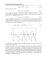
Figure 5(a) shows the CE per solid angle as a function of LP (laser intensity), which was
measured by an EUV energy detector calibrated absolutely—Flying Circus (SCIENTEC
Engineering)—located 45 degrees from the laser incident axis. The laser pulse energy was
0.8 J. We see that the CE was higher under the rotating-drum condition than under the rest
condition. Here, the rest condition is as follows. Xe gas flow is stopped (0 mL/min) after the
target layer has formed, and the drum rests (0 rpm) during a laser shot and stepwise rotates
after every shot so that a fresh target is supplied to the point irradiated by the laser. The
rotation condition is as follows. Laser pulses irradiate quasi-continuously the target on the
rotating drum (>3 rpm), supplying Xe gas (>40 mL/min) and forming the target layer. The
EUV intensity increased immediately with slow rotation (>3 rpm) and appeared to be
almost independent of the rotation speed. In Fig. 5(a), we see that the maximum CE per
solid angle was for an optimized laser intensity of 1 × 10
10
W/cm
2
(LP = –10 mm) during
rotation. The EUV angular distribution could be expressed by a fitting curve of (cos)
0.38
,
and taking into account this distribution, we obtained the maximum spatially integrated CE
of 0.9% at 13.5 nm with 2% bandwidth. EUV spectra at laser intensity of 1 × 10
10
W/cm
2
are
shown in Fig. 5(b). It is obvious that the emission of the 13.5 nm band was greater in the case
of rotation than it was in the case of rest.
Fig. 5. (a) CE at the wavelength of 13.5 nm with 2% bandwidth as a function of LP under the
rotation (130 rpm) and at-rest (0 rpm) conditions. The laser energy was 0.8 J. Insets show the
laser beam focusing on the target. (b) Spectra of EUV radiation from the cryogenic Xe drum
targets under the rotation (bold line) and at-rest (narrow line) conditions with laser intensity
of 1 × 10
10
W/cm
2
for LP of –10 mm.
We considered the mechanism for the increase in EUV intensity with rotation of the target.
Figure 6 shows photographs of the visible emission from the Xe target observed from a
transverse direction. It shows an obvious expansion of the emitting area with longer
(optically thicker) plasma in the rotating case compared with the at-rest case. These images
indicate the existence of any gas on the target surface. Under the rotation condition, Xe gas
is supplied continuously to grow the target layer and the wipers form the layer. However,
the wipers are not chilled especially, and the temperature of the target surface might
increase owing to contact with the wipers in the rotating case so that the vapor pressure
Laser-Plasma Extreme Ultraviolet Source Incorporating a Cryogenic Xe Target
361
increases. Therefore, the vaporized Xe gas from the target surface was considered as the gas
on the target. Although additional Xe gas was added from outside the vacuum chamber, the
EUV intensity did not increase and in fact decreased owing to gas absorption. Therefore, it is
supposed that Xe gas with adequate pressure localizes only near the target surface. From
these results, we conclude that Xe gas on the target surface in the rotating drum produces
optically thick plasma that has optimized density and temperature for emitting EUV
radiation, and satellite lines of the plasma contribute effectively to increasing the EUV
intensity (Sasaki et al., 2004).
Fig. 6. Images of visible emissions from the plasma on the resting (a) and rotating (b) targets.
Next, the dependence of the laser pulse energy was investigated. We measured the CE as a
function of laser energy at different LPs in the rotating drum. For laser energies exceeding
0.3 J, a CE of nearly 0.9% was achieved by tuning the LP with the laser intensity optimized
as ~10
10
W/cm
2
. In the energy range, the maximum CE did not depend on the laser energy.
At the LP in this experiment, the spot size on the target was larger than 500 m and plasma
energy loss at the edges could be ignored for this large spot. Therefore, the same CE was
achieved at the same laser intensity. However, in the lower energy region, the spot size must
be small to achieve optimal laser intensity, and edge loss due to three-dimensional
expansion in plasma cannot then be ignored and a decrease in the CE was observed.
Therefore, it is concluded that laser energy must exceed 0.3 J to achieve a high CE.
The dependence of the laser wavelength was also investigated. Additionally, we carried out 1
double-pulse irradiation experiments in which a pre-pulse produces plasma with optimal
density and temperature, and after a time delay, a main laser pulse effectively injects emission
energy into the expanded plasma to increase the CE. Under the rest condition, there were
increases in CE for the shorter laser or the double pulse irradiation (Miyamoto et al., 2005,
2006). In both cases, the long-scale plasmas and their emission spectra were observed to be
similar to those under the rotation condition for 1 single-pulse irradiation. Therefore, we
supposed that in the both cases, the CE was increased by the same mechanism described
above. However, when the shorter pulses or the double pulses were emitted under the
rotating condition, the CE did not increase but decreased. It is considered that the opacity of
the plasma was too great in these experiments and the best condition was not achieved.
In conclusion, the maximum CE was found to be 0.9% at 13.5 nm with 2% bandwidth for the
optimal condition.
Recent Advances in Nanofabrication Techniques and Applications
362
6. Xe plasma debris
In this section, we report the characteristics of the plasma debris that damages mirrors
(Amano et al., 2010b). First, we investigated fast ions, fast neutrals and ice fragments, which
constitute the debris.
When we found that EUV radiation was greater for a rotating drum than for a drum at rest,
we also found that the number of fast ions decreased simultaneously. Figure 7(a) shows ion
signals from a charge collector (CC) with laser pulse energy of 0.5 J and optimal intensity of
10
10
W/cm
2
, for different drum rotation speeds. The ion signal reduces rapidly after the
drum starts to rotate (> 4 rpm), after which the signal is almost independent of rotation
speed. Ion energy spectra were obtained as shown in Fig. 7(b) using the time-of-flight
signals shown in Fig. 7(a). Here, we assume that all ions were doubly charged because we
measured the principle charge state of Xe ions to be two with an electrostatic energy
analyzer (Inoue et al., 2005). Under the rotation condition, the maximum ion energy
decreases to 6 keV and the number of high-energy ions (with energy of a few dozen kilo-
electron-volts) also decreases. These are favorable characteristics for the debris problem. The
decrease in the ion count under the rotation condition can be explained by a gas curtain effect
that originates from the Xe gas localized at the target surface. The pressure of this localized
Xe gas can be roughly estimated from the peak attenuation () in Fig. 7(a); we estimated the
product of pressure and thickness to be about 10 Pa·mm.
Fig. 7. (a) CC signals of ions and (b) their energy spectra at rotation speeds of 0, 4, 10, 60 and
130 rpm.
in (a) is the loss rate of ions due to the drum rotating. The ion number in (b) was
calculated assuming the charge state was two.
Fast neutral particles were measured by the microchannel plate (MCP) detector when the
number of fast ions decreased under the rotation condition. The MCP is sensitive to both
ions and neutrals, making the use an electric field obligatory to repel ions so that the MCP
detects only neutral particles. From the measurement, we found the number of neutrals to
be approximately an order of magnitude less than the number of ions.
In the case of solid Xe targets, ice fragments might be produced by shock waves of laser
irradiation, whereas this is not the case for gas or liquid targets. In early experiments using a
solid Xe pellet, ice fragments were observed and mirror damage due to these fragments was
Laser-Plasma Extreme Ultraviolet Source Incorporating a Cryogenic Xe Target
363
indicated (Kubiak et al., 1995). Since these reports, liquid Xe targets have been preferred
over solid Xe targets, with the exception of our group. It is therefore necessary to clarify
characteristics of fragment debris from a solid Xe target on a rotating cryogenic drum. After
exposing a Si sample to the Xe plasmas pumped by 100 laser pulses, we observed fragment
impact damage on its surface using a scanning electron microscope. We observed damage
spots on the samples at laser energy of 0.8 J irrespective of whether the drum rotates.
Conversely, we did not observe spots at laser energy of 0.3 J. To explain these results, we
consider that the fragment speed (kinetic energy) might drop below a damage threshold
upon reducing the laser pulse energy because the fragment speed is a function of incident
laser energy (Mochizuki et al., 2001). Observing the damage spots, we know that the
fragment size was larger than a few microns, and the gas curtain might not be effective for
such large fragments. This would explain why the fragment impact damage was
independent of the state of drum rotation. From these results, we conclude that fragment
impact damage, which occurs especially for the solid Xe target, can be avoided simply by
reducing the incident laser pulse energy to less than 0.3 J.
The laser pulse energy was set to 0.3 J to avoid fragment impact damage and the laser
repetition rate was 320 pps, giving an average power of 100 W. Next, we investigated
damage to a Mo/Si mirror, which was the result of total plasma debris (mainly fast ions)
from the laser multi-shots experiments. After 10 min plasma exposure, the sputtered depth
was measured to be 50 nm on the surface of a Mo/Si mirror placed 100 mm from the plasma
at a 22.5-degree angle to the incident laser beam. Because a typical Mo/Si mirror has 40
layer pairs and the thickness of one pair is approximately 6.6 nm, all layers will be removed
within an hour by the sputtering. Although Xe is a deposition-free target, sputtering by
debris needs to be mitigated. However, the major plasma debris component is ions, and we
believe their mitigation to be simple compared with the case of a metal target such as Sn,
using magnetic/electric fields and/or gas. We are now studying debris mitigation by Ar
buffer gas. Ar gas was chosen because of its higher stopping power for Xe ions and lower
absorption of EUV light, and its easy handling and low cost. After the vacuum chamber was
filled with Ar gas, total erosion rates were measured using a gold-coated quartz crystal
microbalance sensor placed 77 mm from the plasma at a 45-degree angle, and
simultaneously, EUV losses were monitored by an EUV detector placed 200 mm from the
plasma at a 22.5-degree angle. Figure 8 shows the erosion rates as a function of Ar gas
pressure. The rates were normalized by the erosion N
0
at a pressure of 0 Pa. When the Ar
pressure was 8 Pa, we found the erosion rate was 1/18 of that without the gas, but the
absorption loss for EUV light was only 8%. The erosion rates (N/N
0
) in Fig. 8 can be fitted to
an exponential curve:
exp
0
P
Ar
NP N l
Ar
kT
(3)
where P
Ar
is the Ar pressure, k is the Boltzmann constant, T is the gas temperature,
is the
cross section and l is the debris flight length. From this fitting, we obtain
= 2.0 × 10
–20
m
2
.
The Ar buffer gas successfully mitigated the effect of plasma debris with little EUV
attenuation. Increasing the Ar pressure, mirror erosion decreases but EUV attenuation
increases. Compromising the erosion and EUV attenuation, an optimized pressure is
achieved. We should localize the higher density Ar gas to only the debris path so that EUV
attenuation is as small as possible. We can design the optimized pressure condition using
Recent Advances in Nanofabrication Techniques and Applications
364
the
value obtained and we consider the use of an Ar gas jet. Through this mitigation, we
expect that erosion will be reduced by more than two orders of magnitude and the lifetime
of the mirror will be extended. We believe the debris problem for Xe plasma will thus be
solved.
Fig. 8. Normalized erosion rate as a function of Ar pressure. The laser energy was 0.3 J and
the rotation speed was 130 rpm.
7. EUV emission at 5-17nm
We began developing the LPP source for EUVL and characterized it at 13.5 nm with 2%
bandwidth, but Xe plasma emission has originally a broad continuous spectrum as shown in
Fig. 9. If the broad emission is used, our source will be very efficient, not limiting its
applications to EUVL. We characterized the source again in the wavelength range of 5–17
nm. Figure 10 shows the CE at 5–17 nm as a function of LP (laser intensity) with laser energy
of 0.8 J. The maximum spatially integrated CE at 5–17 nm was 30% for optimal laser
intensity of 1 × 10
10
W/cm
2
. The maximum CE depended on the laser energy and was 21%
at 0.3 J. Therefore, high average power of 20 W at 5–17 nm has been achieved for pumping
by the slab laser with 100 W (0.3 J at 320 pps). We consider this a powerful and useful
source.
Recently, new lithography using La/B
4
C mirrors having a reflectivity peak at 6.7 nm was
proposed as a next-generation candidate following EUVL using Mo/Si mirrors having a
reflectivity peak at 13.5 nm (Benschop, 2009). This means that a light source emitting around
6 nm will be required in a future lithograph for industrial mass production of
semiconductors. Because our source emits broadly at 5–17 nm as mentioned above, it can
obviously be such a 6 nm light source. We thus next characterized it as a source emitting at
6.7 nm. Here we did not carry out new experiments to optimize the plasma for emitting at
6.7 nm but looked for indications of strong emission at 6.7 nm from the spectrum data
Laser-Plasma Extreme Ultraviolet Source Incorporating a Cryogenic Xe Target
365
already acquired. When making efforts to improve the CE at 13.5 nm, we noticed that
emissions around 6 nm became strong at higher laser intensity. When laser energy is 0.8 J
and LP = 0 mm (i.e., laser intensity is 4 10
12
W/cm
2
under the rotation condition), there is a
hump around 6 nm as shown in Fig. 9. The spatially integrated CE at 6.7 nm with 0.6%
bandwidth is estimated to be 0.1% from this spectrum. Because the bandwidth of 0.6% for
the La/B
4
C mirror reflectivity is narrower than the 2% for the Mo/Si mirror, the available
reflected power is intrinsically small. The CE of 0.1% was not obtained under optimized
conditions and higher CE may be achieved in the future. In any event, our source is only one
LPP source at present that can generate continuously an emission at 6.7 nm.
Fig. 9. Spectra of EUV radiation under the rotation (bold line) and at-rest (narrow line)
conditions with laser intensity of 4 10
12
W/cm
2
for best focus (LP = 0 mm). The laser
energy was 0.8 J.
Fig. 10. CE for a wavelength of 5–17 nm as a function of LP under the rotation (130 rpm)
condition. The laser energy was 0.8 J.
Recent Advances in Nanofabrication Techniques and Applications
366
8. Conclusion
This chapter briefly reviewed our LPP-EUV source. First, we characterized the source at a
wavelength of 13.5 nm with 2% bandwidth as an EUVL source and achieved a maximum CE
of 0.9%. When the driving laser power is 110 W at 320 pps, the average power of 1 W is
obtained at the wavelength and this is thought to be sufficient for the source to be used in
various studies. However, the EUV power required for industrial semiconductor products is
more than 100 W at present; our power is two orders of magnitude less. To approach the
requirements of an industrial EUV source, the remaining tasks are considered. The majority
of Xe plasma debris is fast ions, which can be mitigated using gas and/or a
magnetic/electric field relatively easily. The drum system can supply the Xe target for laser
pulses with energy up to 1 J at 10 kHz. Therefore, a remaining task is powering up the
driving laser. A short pulse laser with average power of the order of 10 kW (i.e., high average
and high peak brightness laser) must be developed and such a breakthrough is much hoped
for.
Not limiting the wavelength to 13.5 nm with 2% bandwidth and using the broad emission at
5–17 nm, a maximum CE of 30% is achieved. Pumping with laser power of 100 W, high
average power of 20 W is already obtained and the source is useful for applications other
than industrial EUVL using Mo/Si mirrors. We are now applying our source to
microprocessing and/or material surface modification. Our source also emits around the
wavelength of 6 nm considered desirable for the next lithography source. In conclusion, our
LPP source is a practicable continuous EUV source having possibilities for various
applications.
9. Acknowledgment
Part of this work was performed under the auspices of MEXT (Ministry of Education,
Culture, Sports, Science and Technology, Japan) under the contract subject "Leading Project
for EUV lithography source development".
10. References
Amano, S., Shimoura, A., Miyamoto, S. & Mochizuki, T. (1997). High-repetition-rate pulse
Nd:YAG slab laser for x-ray source by cryogenic target, 1997 OSA Technical Digest
Series, Vol.11, Conference Edition, CLEO97, p.523, Baltimore, USA, May 18-23, 1997
Amano, S., Shimoura, A., Miyamoto, S. & Mochizuki, T. (1999). Development of a high
repetition rate Nd:YAG slab laser and soft X-ray generation by X-ray cryogenic
target. Fusion Eng. and Design 44, pp.423-426
Amano, S. & Mochizuki, T. (2001). High average and high peak brightness slab laser. IEEE J.
Quantum Electron. 37(2), pp.296-303
Amano, S., Nagano, A.: Inoue, T., Miyamoto, S. & Mochizuki, T. (2008). EUV light sources
by laser-produced plasmas using cryogenic Xe and Li targets. Rev. Laser. Eng.
36(11), pp.715-720 (in Japanese)
Amano, S., Masuda, K., Shimoura, A., Miyamoto, S. & Mochizuki, T. (2010a).
Characterization of a laser-plasma extreme ultraviolet source using a rotating
cryogenic Xe target. Appl. Phys.B 101, pp.213-219
Laser-Plasma Extreme Ultraviolet Source Incorporating a Cryogenic Xe Target
367
Amano, S., Inaoka, Y., Hiraishi, H., Miyamoto, S. & Mochizuki, T. (2010b). Laser-plasma
debris from a rotating cryogenic-solid-Xe target. Rev. Sci. Instrum. 81, pp. 023104-1-
023104-6
Anderson, R.J., Buchenauer, D.A., Klebanoff, L., Wood II, O.R. & Edwards, N.V. (2004). The
erosion of materials exposed to a laser-pulsed plasma (LPP) extreme ultraviolet
(EUV) illumination source, Proceedings of SPIE, Emerging Lithographic Technologies
VIII, vol.5374, pp.710-719, Santa Clara, USA, February 2004
Bakshi,V.(Ed). (2005) EUV Sources for Lithography, SPIE, ISBN:0819458457, Bellingham, WA
Benschop, J. (2009). EUV: past, present and prospects, Keynote I, 2009 International
Symposium on Extreme Ultraviolet Lithography, Prague Czech, October 2009,
International Sematech, Available from: <
/archives/litho/index.htm>
Brandt, D.C., Fomenkov, I.V., Partlo, W.N., Myers, D.W., Kwestens, P., Ershov, A.I.,
Bowering, N.R., Baumgart, P., Bykanov, A.N., Vaschenko, G.O., Khodykin, O.V.,
Srivastava, S., Hou, R., Dea, S.D., Ahmad, I. & Rajyuguru, C. (2010). LPP EUV
source production for HVM, SO-01, 2010 International Symposium on Extreme
Ultraviolet Lithography, Kobe Japan, October 2010, International Sematech, Available
from: <
Fiedorowicz, H., Bartnik, A., Szczurek, M., Daido, H., Sakaya. N., Kmetik, V., Kato, Y.,
Suzuki, M., Matsumura, M., Yajima, J., Nakayma, T. & Wilhein, T. (1999).
Investigation of soft X-ray emission from a gas puff target irradiated with a
Nd:YAG laser, Opt.Comm.,163(1-3), pp.103-114
Fukugaki, K., Amano, S., Shimoura, A., Inoue, T., Miyamoto, S. & Mochizuki, T. (2006).
Rotating cryogenic drum supplying Xe target to generate extreme ultraviolet
radiation. Rev. Sci. Instrum. 77, pp.063114-1-063114-4
Hansson, B.A.M., Hemberg, O., Hertz, M.H., Berglund, M., Choi, H. J., Jacobsson, B., Janin,
E., Mosesson, S., Rymell, L., Thoresen, J. & Wilner, M. (2004). Characterization of a
liquid-xenon-jet laser-plasma extreme-ultraviolet source. Rev.Sci.Instrum. 75(6),
pp.2122-2129
Inoue, T., Kaku, K., Shimoura, A., Nica, P.E., Sekioka, T., Amano, S., Miyamoto, S. &
Mochizuki, T. (2005). Studies on laser-produced plasma EUV generation by using
fast-supplyunig cryogenic Xe targets, 1-SO-10, 2005 International Symposium on
Extreme Ultraviolet Lithography, San Diego, USA, November 2005, International
Sematech, Available from: <
index.htm>
Inoue, T., Amano, S., Miyamoto, S. & Mochizuki, T. (2006). The stability of a rotating-drum
solid-Xe target subjected to high-repetition rate laser irradiation for laser-plasma
EUV generation. Rev. Laser. Eng. 34(8), pp.570-574 (in Japanese)
Inoue, T., Okino, H., Nica, P.E., Amano, S., Miyamoto, S. & Mochizuki, T. (2007). Xe
capillary target for laser-plasma extreme ultraviolet source. Rev. Sci. Instrum. 78,
pp.105105-1-105105-5
Kinoshita, H., Kurihara, K., Ishii,Y. & Torii, Y. (1989). Soft x-ray reduction lithography using
multilayer mirrors. J. Vac. Sci. Technol.B, 7(6), pp.1648-1651
Kubiak, G., Krentz. K., Berger, K., Trucano, T., Fisher, P. & Gouge, M. (1995). Cryogenic
pellet laser plasma source targets, OSA Proceedings on Soft X-ray Projection
Lithography, vol.23, pp.248-254, Monterey, USA, September 1994
Recent Advances in Nanofabrication Techniques and Applications
368
Kubiak, G., Bernardez, L.J., Krenz, K.D., O’Connell, D.J., Gutowski, R. & Todd, A.M., (1996).
Debris-free EUVL sources based on gas jets, OSA TOPS on Extreme Ultraviolet
Lithography, vol.4, pp.66-71
Miyamoto, S., Shimoura, A., Amano, S., Fukugaki, K., Kinugasa, H., Inoue, T. & Mochizuki,
T. (2005). Laser wavelength and spot diameter dependence of extreme ultraviolet
conversion efficiency in , 2, and 3 Nd:YAG laser-produced plasmas. Appl. Phys.
Lett. 86(26), pp.261502-1-261502-3
Miyamoto, S., Amano, S.: Inoue, T., Nica, P. E., Shimoura, A., Kaku, K., Sekioka, T. &
Mochizuki, T. (2006). EUV source developments on laser-produced plasmas using
cryogenic Xe and Lithium new scheme target, Proceedings of SPIE, Emerging
Lithographic Technologies X, vol.6151, pp.61513S-1-61513S-10, San Jose, USA,
February 2006
Mizoguti, H., Abe, T., Watanabe, Y., Ishihara, T., Ohta, T., Hori, T., Kurosu, A., Komori, H.,
Kakizaki, K., Sumitani, A., Wakabayashi, O., Nakarai, H., Fujimoto, J. & Endo, A.
(2010). 1
st
generation laser-produced plasma 100W source system for HVM EUV
lithography, SO-03, 2010 International Symposium on Extreme Ultraviolet Lithography,
Kobe Japan, October 2010, International Sematech, Available from: <http://www.
sematech.org/meetings/archives/litho/index.htm>
Mochizuki, T., Shimoura, A., Amano, S. & Miyamoto, S. (2001). Compact high-average-
power X-ray source by cryogenic target, Proceedings of SPIE, Applications of X Rays
Generated from Lasers and Other Bright Sources II, vol.4504, pp.87-96, San Diego, USA,
July 2001
Sasaki, A., Nishihara, K., Murakami, M., Koike, F., Kagawa, T., Nishikawa, T., Fujima, K.,
Kawamura, T. & Furukawa, H. (2004). Effect of the satellite lines and opacity on the
extreme ultraviolet emission from high-density Xe plasmas. Appl. Phys. Lett. 85(24),
pp.5857-5859
Shimoura, A., Amano, S., Miyamoto, S. & Mochizuki, T. (1998). X-ray generation in
cryogenic targets irradiated by 1 m pulse laser. Appl. Phys. Lett. 72(2), pp.164-166
Soumagne, G.: Abe, T., Suganuma,T. , Imai, Y., Someya, H., Hoshino, H., Nakano, M.,
Komori, H., Takabayashi, Y., Ariga, T., Ueno, Y., Wada, Y., Endo, A & Toyoda,
K.(2005). Laser-produced-plasma light source for EUV lithography, Proceedings of
SPIE, Emerging Lithographic Technologies IX, vol.5751, pp.822-828, San Jose, USA,
March 2005
19
Irradiation Effects on EUV Nanolithography
Collector Mirrors
J.P. Allain
Purdue University
United States of America
1. Introduction
Exposure of collector mirrors facing the hot, dense pinch plasma in plasma-based EUV light
sources to debris (fast ions, neutrals, off-band radiation, droplets) remains one of the highest
critical issues of source component lifetime and commercial feasibility of nanolithography at
13.5-nm. Typical radiators used at 13.5-nm include Xe, Li and Sn. Fast particles emerging
from the pinch region of the lamp are known to induce serious damage to nearby collector
mirrors. Candidate collector configurations include either multi-layer mirrors (MLM) or
single-layer mirrors (SLM) used at grazing incidence. Due to the strong absorbance of 13.5-
nm light only reflective optics rather than refractive optics can work in addition to the need
for ultra-high vaccum conditions for its transport.
This chapter presents an overview of particle-induced damage and elucidates the
underlying mechanisms that hinder collector mirror performance at 13.5-nm facing high-
density pinch plasma. Results include recent work in a state-of-the-art in-situ EUV
reflectometry system that measures real time relative EUV reflectivity (15-degree incidence
and 13.5-nm) variation during exposure to simulated debris sources such as fast ions,
thermal atoms, and UV radiation (Allain et al., 2008, 2010). Intense EUV light and off-band
radiation is also known to contribute to mirror damage. For example off-band radiation can
couple to the mirror and induce heating affecting the mirror’s surface properties. In
addition, intense EUV light can partially photoionize background gas used for mitigation in
the source device. This can lead to local weakly ionized plasma creating a sheath and
accelerating charged gas particles to the mirror surface inducing sputtering. In this overview
we will also summarize studies of thermal and energetic particle exposure on collector
mirrors as a function of temperature simulating the effects induced by intense off-band and
EUV radiation found in EUVL sources. Measurements include variation of EUV reflectivity
with mirror damage and in-situ surface chemistry evolution.
In this chapter the details from the EUV radiation source to the collector mirror are linked in
the context of mirror damage and performance (as illustrated in Figure 1). The first section
summarizes EUV radiation sources and their performance requirements for high-volume
manufacturing. The section compares differences between conventional discharge plasma
produced (DPP) versus laser plasma produced (LPP) EUV light sources and their possible
combinations. The section covers the important subject of high-density transient plasmas
and their interaction with material components. The different types of EUV radiators, debris
Recent Advances in Nanofabrication Techniques and Applications
370
distribution, and mitigation sources are outlined. The second section summarizes the
various optical collector mirror geometries used for EUV lithography. A brief discussion on
the intrinsic damage mechanisms linked to their geometry is included. The third section
summarizes in general irradiation-driven mechanisms as background for the reader and its
relation to the “quiescent” plasma collector mirrors are exposed in EUV sources. This
includes irradiation-driven nanostructures, sputtering, ion mixing, surface diffusion, and
ion-induced surface chemistry. The fourth section briefly discusses EUV radiation-driven
plasmas as another source of damage to the mirror. These plasmas are a result of using
gases for debris mitigation. The fifth section is a thorough coverage of the key irradiation-
driven damage to optical collector mirrors and their performance limitations as illustrated in
part by Figure 1.
2. EUV radiation sources
There are numerous sources designed to generate light at the extreme ultraviolet line of
13.5-nm. Historically advanced lithography has considered wavelength ranges from hard X-
rays up to 157 nm [Bakshi, 2009]. Radiators of 13.5-nm light rely on high-density plasma
generation typically based on discharge-produced configurations with magnetically
confined high-density plasmas or laser-produced plasmas. Recently, some sources have
combined both techniques (Banine 2011). Generation of high-density plasmas to yield
temperatures of the order of 10-50 eV require advanced materials for plasma-facing
components in these extreme environments in particular discharge-produced plasma (DPP)
configurations. This is due to the need of metallic anode/cathode components operating
under high-heat flux conditions. Laser-produced plasmas (LPP) benefits from the fact that
no nearby electrodes are necessary to induce the plasma discharge. Further details will be
described in section 5.1. One challenge in operating EUV lamps at high power is the
collected efficiency of photons at the desired exposure wavelength of 13.5-nm. This
particular line has a number of radiators with properties that have consequences on EUV
source operation. For example radiators at 13.5-nm include xenon, tin and lithium. The latter
two are metals and thus their operation complicated by contamination issues on nearby
material components such as electrodes and collector mirrors. Further discussion follows in
section 2.2 and 2.3. To contend with the various types of debris that are generated in the
plasma-producing volume a variety of novel debris mitigation systems (DMS) have been
designed and developed for both DPP and LPP configurations.
2.1 Function and material components
The transient nature of the high-density plasma environment in DPP and LPP systems
results in exposure of plasma-facing components to extreme conditions (e.g. high plasma
density (~ 10
19
cm
-3
) and temperature (~ 20-40 eV). However, in LPP systems since the
configuration is mostly limited by the mass of the radiator and the laser energy supplied to
it to generate highly ionized plasma with the desired 13.5-nm light. Both configurations rely
on efficient radiators of 13.5-nm light, which include: Li, Sn and Xe. In DPP designs a variety
of configurations have been used that include: dense plasma focus, capillary Z-pinch, star
pinch, theta pinch and hollow cathode among others. For a more formal description of these
high-density plasma sources for 13.5-nm light generation the author refers to the recent
publications by V. Bakshi in 2006 and 2009 (Bakshi, 2006; Bakshi, 2009).
Irradiation Effects on EUV Nanolithography Collector Mirrors
371
The in-band and off-band radiation generated in these sources is also a critical limitation in
operation of these lamps since on average the off-band radiation is converted into heat on
nearby plasma-facing components. There are additional challenges in the design of 13.5-nm
light sources that include: high-frequency operation limits driven by the need to extract high
EUV power at the intermediate focus (IF) and limited by the available high-throughput
power of the plasma device (e.g. laser system or discharge electrode system). Additionally,
the scaling of debris with EUV power extraction and the limitation of conversion efficiency
(CE) with source plasma size also translate into significant engineering challenges to the
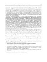
design of 13.5-nm lithography source design. Figure 1 illustrates, for the case of the DPP
configuration, the primary debris-generating sources that compromise 13.5-nm collector
mirrors. The first region depicted on the left is defined here as the “transient plasma
region”. This is the region described earlier with high-density and high-temperature plasma
interacting with the electrode surfaces.
Fig. 1. Illustration of the various components of EUV 13.5-nm radiation source configuration
consisting primarily of three major components: 1) plasma radiator section, 2) debris
mitigation system and 3) optical collector mirror.
In DPP discharge sources material components that make up the electrode system consist of
high-temperature, high-toughness materials. Although DPP source design has traditionally
used high-strength materials such as tungsten and molybdenum alloys, the extreme
conditions in these systems limit the operational lifetime of the electrode. Significant
plasma-induced damage is found in the electrode surfaces, which induce degradation and
abrasion over time. Figure 2, for example, shows a scanning electron micrograph of a
tungsten electrode exposed to a dense plasma focus high-intensity plasma discharge. The
key feature in the SEM image is the existence of plasma-induced damage domains that
effectively have induced melting in certain sections of the electrode surface.
Recent Advances in Nanofabrication Techniques and Applications
372
The second region depicted in Figure 1 is defined as the debris mitigation zone (DMZ). In
this region a variety of debris mitigation strategies can be used to contend with the large
debris that exists in operation of the DPP source. For example the use of inert gas to slow-
down energetic particles that are generated in the pinch plasma region and/or debris
mitigation shields that collect macro-scale particulates when using Sn-based radiators in
DPP devices. Radiation-induced mechanisms on the surfaces of the DMZ elements also can
lead to ion-induced sputtering of DM shield material that eventually is deposited in the
nearby 13.5-nm collector mirror. Therefore care is taken to select sputter-resistant materials
for the DM shields used such as refractory metal alloys and certain stainless steels. Design of
DM shields also involve computational modeling that can aid in identifying appropriate
materials depending on the source operation and generation of a variety of debris types
such as clusters, ions, atoms, X-rays, electrons and macroscopic dust particles.
Fig. 2. SEM micrographs of a tungsten electrode exposed to high-intensity plasma during
the generation of EUV 13.5-m light.
The third region in Fig. 1 consists of the 13.5-nm light collector mirror. The collector mirror
has a configuration to optimally collect as much of the 13.5-nm light as possible. Its function
is to deliver EUV power in a specified etendue at the intermediate focus (IF) or the opening
of the illuminator. This power is in turn dictated by the specification on EUV exposure of
the EUV lithography scanner that must be able to operate with 150-200 wafers per hour
(wph) at nominal power for periods of 1-2 years without maintenance (so-called high-
volume manufacturing, HVM, conditions). This ultra-stringent requirement is one of the
primary challenges to EUV lithography today. Since powers of order 200-300 W at the IF
need to be sustained for a year or more, materials at the DPP source and those used for
collector mirrors will necessarily require revolutionary advances in materials performance.
The third region in Figure 1 also depicts what debris the collector mirror is exposed to
during the discharge. A distribution of debris energies (i.e. ions), fluxes and masses will
effectively affect the mirror surface performance. The third region is also known as the
“condenser or collector optics region”.
2.2 Selection of electrode materials in DPP EUV devices
Selection of materials for DPP electrodes depends on the microstructure desired to minimize
erosion and maximize thermal conductivity. Figure 3 shows an example of SEM
micrographs of materials identified to have promising EUV source electrode properties. The
powder composite materials inherited the structural characteristics of the initial powders,
determined by the processes of combined restoration of tungsten and nickel oxides (WO
3
Irradiation Effects on EUV Nanolithography Collector Mirrors
373
and NiO from NiCO
3
, for instance) and copper molybdate (MoCuO
4
). Dry hydrogen (the
dew point temperature is above 20
0
C) facilitates the formation of the heterogeneous
conglomerates in W-Ni-powders, which do not collapse at sintering or saturate the material
(Figure 3a), and spheroidizing of molybdenum particles and re-crystallization through the
liquid phase in the conditions of sintering the composite consisting of molybdenum and
copper (Figure 3b). For comparison, the structure is shown in Figure 3c obtained from tested
W-Ni powders. The structure of the materials was studied by means of scanning electron
microscopy (SEM) of the secondary electrons. A variety of materials characterization
including surface spectroscopy and X-ray based diffraction is used to assess the condition of
the materials after processing with sintering-based techniques. The powder composite
materials are so-called pseudo alloys, which provide promising high thermal conductivity
properties, while displaying sub-unity sputter yields (see Section 4).
Fig. 3. From left to right, (a) the structure of the W-Cu-Ni-LaB6 pseudo alloy (x540), (b) the
structure of the Cu-44%Mo – 1%LaB6 pseudo alloy (x2000), and (c) the structure of
“irradiated” W-Cu-Ni pseudo alloy produced by class W-Ni powder (x400).
Observations made with secondary mass ion spectrometry (SIMS) on these materials found
evidence of hydrogen and beryllium in anode components. Based on these results one can
speculate that the hydrogen observed by SIMS after exposing the samples may be caused by
that environment, in which the powders are manufactured, sintered, and additionally
annealed. In regards to the beryllium observed on the anode surface after exposure to the
xenon plasma, one may suppose two possible explanations, each of which requires
additional verification. The construction may contain beryllium bronze; or the construction
may contain Al
2
0
3
or BeO based ceramics. Both cases may be the reason for enrichment of
the surface samples by these elements during the heating phases.
For systems with the absence of the component interactions, the arc xenon plasma impact
to the electrode materials does not cause a noticeable change of durability: for MoCuLaB
6:
HV = 1600-1690 MPa; and for Cu- Al
2
O
3
: HV = 660 MPa through the whole height of the
anode. In the tungsten and copper based composites, when presence of nickel exists, the
mutual dissolution of the elements is increased (W is dissolved in Cu-Ni melt, for
instance). At cooling, it may be accompanied by either forming non-equilibrium solid
solution, or solidification; which is conformed by the increasing the firmness of the upper
part of the anode (3380 MPa compared to 3020 MPa in its lower part). To provide more
careful analysis, one should investigate the dependence of electro-conductive composites
on heat resistance subject to arc discharges of powerful heat fluxes (up to 10
7
W/m
2
).
Additional analyses typically conducted include the propagation of cracks, observed on
the surface layer of the anode material and deep into the bulk. For that, the precise
method of manufacturing is required for further insight on crack development and
Recent Advances in Nanofabrication Techniques and Applications
374
propagation. These analyses along with erosion material modeling (discussed in Section
4) are mainly used to dictate materials selection for electrode materials in EUV DPP
sources.
2.3 EUV radiators, debris generation and debris mitigation systems
One particularly important “coupling” effect between the debris mitigation zone region and
the collector optics region is the use of inert mitigation gases (e.g. Ar or He) that in turn are
ionized by the expanding radiation field and thus generate low-temperature plasma near
the collector mirror surface. This phenomenon is briefly discussed in Section 3. Each
candidate radiator (e.g. Li, Sn or Xe or any combination) will result in a variety of
irradiation-induced mechanisms at the collector mirror surface. For example, if one
optimizes the EUV 13.5-nm light source for Li radiators, the energy, flux and mass
distributions will be different compared to Sn. Both of these in turn are also different from
the standpoint of contamination given that both are metallic impurities and Xe is an inert
gas. The former will lead to deposition of material on the mirror surface. In the case of Xe,
thermal deposition would be absent however the energetic Xe implantation on the mirror
surface could lead to inert gas damage such as surface blistering and gas bubble production
for large doses. Debris mitigation systems would have to be designed according to the
radiator used.
3. EUV radiation-driven plasmas
As discussed earlier, Figure 1 shows the general configuration of a DPP system for EUV
13.5-nm light generation. Another “coupling” effect of the DMZ in the source system (e.g.
from the electrode materials of the source through the DMZ to the collector mirror) is the
fact that the intense EUV and UV radiation generated from the 13.5-nm radiators (e.g. Xe or
Sn) can induce a secondary low-temperature plasma at the surface of the collector mirror by
ionizing the protective gas used for debris mitigation such as argon or helium [Van der
Velden et al, 2006, Van der Velden & Lorenz, 2008]. The characteristic plasma in this region
is found to be of low temperature (e.g. 5-10 eV) and moderate densities (e.g. ~ 10
16
cm
-3
). The
photoionization process can lead to fast electrons that induce a voltage difference the order
of 70 V. In addition, due to the sheath region at the plasma-material interface between the
plasma and the mirror the ionized gas particles (e.g. Ar
+
or He
+
) can be accelerated up to
about 50-60 eV. This energy in the case of Ar ions is relatively low and in the so-called
sputter threshold regime for bombardment on candidate collector mirror material
candidates. In addition, carbon contamination could also be accompanied by this plasma
exposure. These candidate materials are typically thin (~20-60 nm) single layers of Ru, Rh or
Pd, all of which reflect 13.5-nm light very efficiently. Only few studies have been conducted
to elucidate how these low-energy ions may induce changes that can degrade the optical
properties of the 13.5-nm collector mirrors. Van der Velden and Allain studied this effect in
detail in the in-situ experimental facility known as IMPACT to determine the sputter
threshold levels at similar energies [Allain et al, 2007]. In the work by van der Velden et al.
the threshold sputtering of ruthenium mirror surface films were found to be in close
agreement with theoretical models by Sigmund and Bohdansky. The sputter yields varied
between 0.01-0.05 atoms/ion for energies about 50-100 eV and models were found to be
within 10-15% of these values.
Irradiation Effects on EUV Nanolithography Collector Mirrors
375
4. Irradiation-driven mechanisms on material surfaces
Before discussion of collector mirror geometry and configuration a brief background on
irradiation-driven mechanism on material surfaces is in order. In DPP EUV devices
electrodes at the source are exposed to short (10-20 nsec) high-intensity plasmas leading
to a variety of erosion mechanisms. Erosion of the electrodes is dictated by the dynamics
of the plasma pinch for configurations such as: dense plasma focus, Z-pinch and capillary.
The transient discharge deposits 1-2 J/cm
2
per pulse on electrode surfaces. Large heat flux
is deposited at corners and edges leading to enhanced erosion. Understanding of how
particular materials respond to these conditions is part of rigorous design of DPP
electrode systems. Erosion mechanisms can include: physical sputtering, current-induced
macroscopic erosion, melt formation, droplet, and particulate ejection [Hassanein et al,
2008]. Erosion at the surface is also governed by the dynamics of how plasma can generate
a vapor cloud leading to a self-shielding effect, which results in ultimate protection of the
surface bombarded. Determining whether microscopic erosion mechanisms such as:
physical sputtering or macroscopic mechanisms such as melt formation and droplet
ejection the dominant material loss mechanism remains an open question in DPP
electrode design. This is because such mechanisms are inherently dependent on the pinch
dynamics and operation of the source. One important consequence of the extreme
conditions electrode and collector optics surfaces are exposed is the existence of several
irradiation-driven mechanisms that can lead to substantial materials mixing at the
plasma-material interface. Bombarment-induced modification of materials can in
principle lead to phase transition mechanisms that can substantially change the
mechanical properties of the material accelerating degradation.
Conceptually, the phenomenon of bombardment-induced compositional changes is simplest
when only athermal processes exist such as: preferential sputtering (PS) and collisional
mixing (CM). Preferential sputtering occurs in most multi-component surfaces due to
differences in binding energy and kinematic energy transfer to component atoms near the
surface. Collisional mixing of elements in multi-component materials is induced by
displacement cascades generated in the multi-component surface by bombarding
particles/clusters and is described by diffusion-modified models accounting for irradiation
damage. Irradiation can accelerate thermodynamic mechanisms such as Gibbsian
adsorption or segregation (GA) leading to substantial changes near the surface with spatial
scales of the order of the sputter depth (few monolayers). GA occurs due to thermally
activated segregation of alloying elements to surfaces and interfaces reducing the free
energy of the alloy system. Typically, GA will compete with PS and thus, in the absence of
other mechanisms, the surface reaches a steady-state concentration approaching that of the
bulk. However when other mechanisms are active, synergistic effects can once again alter
the near-surface layer and complex compositions are achieved. These additional
mechanisms include: radiation-enhanced diffusion (RED) due to the thermal motion of non-
equilibrium point defects produced by bombarding particles near the surface, radiation-
induced segregation (RIS), a result of point-defect fluxes, which at sufficiently high
temperatures couples defects with a particular alloying element leading to compositional
redistribution in irradiated alloys both in the bulk and near-surface regions. Figure 4 shows
the temperature regime where these mechanisms are dominant. All of these mechanisms
must be taken under account in the design of proposed advanced materials for the
electrodes and the collector optics in addition to considering other bombardment-induced