Sequential Verulog Topics part 9 ppsx
Bạn đang xem bản rút gọn của tài liệu. Xem và tải ngay bản đầy đủ của tài liệu tại đây (43.09 KB, 5 trang )
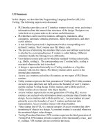
13.5 Summary
In this chapter, we described the Programming Language Interface (PLI) for
Verilog. The following aspects were discussed:
• PLI Interface provides a set of C interface routines to read, write, and extract
information about the internal data structures of the design. Designers can
write their own system tasks to do various useful functions.
• PLI Interface can be used for monitors, debuggers, translators, delay
calculators, automatic stimulus generators, dump file generators, and other
useful utilities.
• A user-defined system task is implemented with a corresponding user-
defined C routine. The C routine uses PLI library calls.
• The process of informing the simulator that a new user-defined system task
is attached to a corresponding user C routine is called linking. Different
simulators handle the linking process differently.
• User-defined system tasks are invoked like standard Verilog system tasks,
e.g., $hello_verilog(); . The corresponding user C routine hello_verilog is
executed whenever the task is invoked.
• A design is represented internally in a Verilog simulator as a big data
structure with sets for objects. PLI library routines allow access to the
internal data structures.
• Access (acc) routines and utility (tf) routines are two types of PLI library
routines.
• Utility routines represent the first generation of Verilog PLI. Utility routines
are used to pass data back and forth across the boundary of user C routines
and the original Verilog design. Utility routines start with the prefix tf_.
Utility routines do not interact with object handles.
• Access routines represent the second generation of Verilog PLI. Access
routines can read and write information about a particular object from/to the
design. Access routines start with the prefix acc_. Access routines are used
primarily across the boundary of user C routines and internal data
representation. Access routines interact with object handles.
• Value change link (VCL) is a special category of access routines that allow
monitoring of objects in a design. A consumer routine is executed whenever
the monitored object value changes.
• Verilog Procedural Interface (VPI) routines represent the third generation of
Verilog PLI. VPI routines provide a superset of the functionality of acc_ and
tf_ routines. VPI routines are not covered in this book.
Programming Language Interface is a very broad area of study. Thus, only the
basics of Verilog PLI are covered in this chapter. Designers should consult the
IEEE Standard Verilog Hardware Description Language document for details of
PLI.
[ Team LiB ]
[ Team LiB ]
13.6 Exercises
Refer to Appendix B
, List of PLI Routines and IEEE Standard Verilog Hardware
Description Language document, for a list of PLI access and utility routines, their
function, and usage. You will need to use some PLI library calls that were not
discussed in this chapter.
1:
Write a user-defined system task, $get_in_ports, that gets full hierarchical
names of only the input ports of a module instance. Hierarchical module
instance name is the input to the task (Hint: Use the C routine in Example
13-2 as a reference). Link the task into the Verilog simulator. Find the
input ports of the 1-bit full adder defined in Example 5-7
on page 75.
2:
Write a user-defined system task, $count_and_gates, which counts the
number of and gate primitives in a module instance. Hierarchical module
instance name is the input to the task. Use this task to count the number of
and gates in the 4-to-1 multiplexer in Example 5-5
.
3:
Create a user-defined system task, $monitor_mod_output, that finds out all
the output signals of a module instance and adds them to a monitoring list.
The line "Output signal has changed" should appear whenever any output
signal of the module changes value. (Hint: Use VCL routines.) Use the 2-
to-1 multiplexer in Example 13-1
. Add output signals to the monitoring
list by using $monitor_mod_output. Check results by applying stimulus.
[ Team LiB ]
[ Team LiB ]
14.1 What Is Logic Synthesis?
Simply speaking, logic synthesis is the process of converting a high-level
description of the design into an optimized gate-level representation, given a
standard cell library and certain design constraints. A standard cell library can have
simple cells, such as basic logic gates like and, or, and nor, or macro cells, such as
adders, muxes, and special flip-flops. A standard cell library is also known as the
technology library. It is discussed in detail later in this chapter.
Logic synthesis always existed even in the days of schematic gate-level design, but
it was always done inside the designer's mind. The designer would first understand
the architectural description. Then he would consider design constraints such as
timing, area, testability, and power. The designer would partition the design into
high-level blocks, draw them on a piece of paper or a computer terminal, and
describe the functionality of the circuit. This was the high-level description.
Finally, each block would be implemented on a hand-drawn schematic, using the
cells available in the standard cell library. The last step was the most complex
p
rocess in the design flow and required several time-consuming design iterations
before an optimized gate-level representation that met all design constraints was
obtained. Thus, the designer's mind was used as the logic synthesis tool, as
illustrated in Figure 14-1
.
Figure 14-1. Designer's Mind as the Logic Synthesis Tool
The advent of computer-aided logic synthesis tools has automated the process of
converting the high-level description to logic gates. Instead of trying to perform
logic synthesis in their minds, designers can now concentrate on the architectural
trade-offs, high-level description of the design, accurate design constraints, and
optimization of cells in the standard cell library. These are fed to the computer-
aided logic synthesis tool, which performs several iterations internally and
generates the optimized gate-level description. Also, instead of drawing the high-
level description on a screen or a piece of paper, designers describe the high-level
design in terms of HDLs. Verilog HDL has become one of the popular HDLs for
the writing of high-level descriptions. Figure 14-2
illustrates the process.
Figure 14-2. Basic Computer-Aided Logic Synthesis Process
Automated logic synthesis has significantly reduced time for conversion from
high-level design representation to gates. This has allowed designers to spend more
time on designing at a higher level of representation, because less time is required
for converting the design to gates.
[ Team LiB ]
[ Team LiB ]
14.2 Impact of Logic Synthesis
Logic synthesis has revolutionized the digital design industry by significantly
improving productivity and by reducing design cycle time. Before the days of
automated logic synthesis, when designs were converted to gates manually, the
design process had the following limitations:
• For large designs, manual conversion was prone to human error. A small
gate missed somewhere could mean redesign of entire blocks.
• The designer could never be sure that the design constraints were going to be
met until the gate-level implementation was completed and tested.
• A significant portion of the design cycle was dominated by the time taken to
convert a high-level design into gates.
• If the gate-level design did not meet requirements, the turnaround time for
redesign of blocks was very high.
• What-if scenarios were hard to verify. For example, the designer designed a
block in gates that could run at a cycle time of 20 ns. If the designer wanted
to find out whether the circuit could be optimized to run faster at 15 ns, the
entire block had to be redesigned. Thus, redesign was needed to verify what-
if scenarios.
• Each designer would implement design blocks differently. There was little
consistency in design styles. For large designs, this could mean that smaller
blocks were optimized, but the overall design was not optimal.
• If a bug was found in the final, gate-level design, this would sometimes
require redesign of thousands of gates.
• Timing, area, and power dissipation in library cells are fabrication-
technology specific. Thus if the company changed the IC fabrication vendor
after the gate-level design was complete, this would mean redesign of the
entire circuit and a possible change in design methodology.
• Design reuse was not possible. Designs were technology-specific, hard to
port, and very difficult to reuse.
Automated logic synthesis tools addressed these problems as follows:
• High-level design is less prone to human error because designs are described
at a higher level of abstraction.
• High-level design is done without significant concern about design
constraints. Logic synthesis will convert a high-level design to a gate-level
netlist and ensure that all constraints have been met. If not, the designer goes
back, modifies the high-level design and repeats the process until a gate-
level netlist that satisfies timing, area, and power constraints is obtained.
• Conversion from high-level design to gates is fast. With this improvement,
design cycle times are shortened considerably. What took months before can
now be done in hours or days.
• Turnaround time for redesign of blocks is shorter because changes are
required only at the register-transfer level; then, the design is simply
resynthesized to obtain the gate-level netlist.
• What-if scenarios are easy to verify. The high-level description does not
change. The designer has merely to change the timing constraint from 20 ns
to 15 ns and resynthesize the design to get the new gate-level netlist that is
optimized to achieve a cycle time of 15 ns.
• Logic synthesis tools optimize the design as a whole. This removes the
problem with varied designer styles for the different blocks in the design and
suboptimal designs.
• If a bug is found in the gate-level design, the designer goes back and
changes the high-level description to eliminate the bug. Then, the high-level
description is again read into the logic synthesis tool to automatically
generate a new gate-level description.
• Logic synthesis tools allow technology-independent design. A high-level
description may be written without the IC fabrication technology in mind.
Logic synthesis tools convert the design to gates, using cells in the standard
cell library provided by an IC fabrication vendor. If the technology changes
or the IC fabrication vendor changes, designers simply use logic synthesis to
retarget the design to gates, using the standard cell library for the new
technology.
• Design reuse is possible for technology-independent descriptions. For
example, if the functionality of the I/O block in a microprocessor does not
change, the RTL description of the I/O block can be reused in the design of
derivative microprocessors. If the technology changes, the synthesis tool
simply maps to the desired technology.