Electric Circuits, 9th Edition P24 potx
Bạn đang xem bản rút gọn của tài liệu. Xem và tải ngay bản đầy đủ của tài liệu tại đây (957.8 KB, 10 trang )
206 Inductance, Capacitance, and
Mutual
Inductance
t = 0 the inductor was switched instantaneously to
position b where it remained for 1.6
s
before returning
instantaneously to position a. The d'Arsonval volt-
meter has a full-scale reading of
20
V and a sensitivity
of 1000 ft/V. What will the reading of the voltmeter
be at the instant the switch returns to position a if the
inertia of the d'Arsonval movement is negligible?
Figure P6.13
3mV
+)
Voltmeter
PSPICE
HULTISIH
Section 6.2
6.14 The current shown in Fig. P6.14 is applied to a
0.25 /xF capacitor. The initial voltage on the capaci-
tor is zero.
a) Find the charge on the capacitor at t = 15 /xs.
b) Find the voltage on the capacitor at t = 30 /xs.
c) How much energy is stored in the capacitor by
this current?
Figure P6.14
i (mA)
t (fis)
6.15 The initial voltage on the 0.5 /xF capacitor shown in
PSPICE
Fig. P6.15(a) is -20 V. The capacitor current has
mnsm
the waveform shown in Fig. P6.15(b).
a) How much energy, in microjoules, is stored in
the capacitor at t = 500 /xs?
b) Repeat (a) for t = oo.
6.16 The rectangular-shaped current pulse shown in
PSPICE pig. P6.16 is applied to a 0.1 fxF capacitor. The ini-
' tial voltage on the capacitor is a 15 V drop in the
reference direction of the current. Derive the
expression for the capacitor voltage for the time
intervals in (a)-(d).
a) 0 < t <
10
/xs;
b) 10/AS < t =5 20/xs;
c) 20
/xs
< t < 40 /xs
d) 40 /xs < t < oo
c) Sketch v{t) over the interval -10 /xs ^ t ^ 50 ju.s.
Figure P6.16
i (mA)
160
PSPICE
MULTISIM
100
0
50
10
20 30 40
t(fJLS)
6.17 A 20 fxF capacitor is subjected to a voltage pulse
having a duration of 1 s. The pulse is described by
the following equations:
30t
2
V,
<30(f-
1)
2
V,
0
0 < t < 0.5 s;
0.5 s < t < 1 s;
elsewhere.
Sketch the current pulse that exists in the capacitor
during the
1
s interval.
6.18 The voltage across the terminals of a 0.2 /xF capaci-
tor is
v =
150 V, t < 0;
(Ate**** +
A*T
saiDt
)V,
t>0.
Figure P6.15
0.5
/xF
-20 V
v
(a)
i
(n
50
25
0
lA)
I
100
50e-
20()()
'mA,/>0
1 1 1 l
200
300 400 500
f(jiS)
(b)
Problems 207
6.19
PSPICE
MULTISIM
V =
The initial current in the capacitor is 250 mA.
Assume the passive sign convention.
a) What is the initial energy stored in the capacitor?
b) Evaluate the coefficients A
{
and A
2
.
c) What is the expression for the capacitor current?
The voltage at the terminals of the capacitor in
Fig. 6.10 is known to be
-20 V, / < 0;
100 - 40^
200()
'(3 cos 1000? + sin 1000/) V t > 0.
Assume C = 4 /xF.
a) Find the current in the capacitor for t < 0.
b) Find the current in the capacitor for t > 0.
c) Is there an instantaneous change in the voltage
across the capacitor at t = 0?
d) Is there an instantaneous change in the current
in the capacitor at t = 0?
e) How much energy (in millijoules) is stored in
the capacitor at t = oo?
Section 6.3
6.20 Assume that the initial energy stored in the induc-
PSPICE tors of Fig. P6.20 is zero. Find the equivalent induc-
tance with respect to the terminals a,b.
Figure P6.20
30FH20H
10
H 8H
6.21 Assume that the initial energy stored in the induc-
tors of Fig. P6.21 is zero. Find the equivalent induc-
tance with respect to the terminals a,b.
Figure P6.21
3H
8H
6.22 Use realistic inductor values from Appendix H to con-
struct series and parallel combinations of inductors to
yield the equivalent inductances specified below. Try
to minimize the number of inductors used. Assume
that no initial energy is stored in any of the inductors.
a) 3mH
b) 250/xH
c) 6QfxH
6.23 The three inductors in the circuit in Fig. P6.23 are con-
PSPICE nected across the terminals of a black box at t = 0.
The resulting voltage for t > 0 is known to be
v
a
= 2000e"
100
' V.
If /,(0) = -6Aand/
2
(0) = 1 A, find
a) U0);
b) U0, t > 0;
c) ii(f)»*
s
0;
d)
/
2
(/),
t > 0:
e) the initial energy stored in the three inductors;
f) the total energy delivered to the black box; and
g) the energy trapped in the ideal inductors.
Figure P6.23
6.24 For the circuit shown in Fig.
P6.23,
how many milli-
seconds after the switch is opened is the energy
delivered to the black box 80% of the total energy
delivered?
6.25 The two parallel inductors in Fig. P6.25 are con-
nected across the terminals of a black box at t = 0.
The resulting voltage v for t > 0 is known to be
64e
-4
'
V. It is also known that /,(0) = -10 A and
/
2
(0) = 5 A.
a) Replace the original inductors with an equiva-
lent inductor and find /(f) for f > 0.
b) Find *',(*) for t > 0.
c) Find i
2
(t) for t > 0.
d) How much energy is delivered to the black box
in the time interval 0 < f < oo?
e) How much energy was initially stored in the par-
allel inductors?
f) How much energy is trapped in the ideal inductors?
g) Show that your solutions for /, and /
2
agree with
the answer obtained in (f).
Figure P6.25
208 Inductance, Capacitance, and
Mutual
Inductance
6.26 Find the equivalent capacitance with respect to the
terminals a,b for the circuit shown in Fig. P6.26.
30 V + - OV +
6.27 Find the equivalent capacitance with respect to the
terminals a,b for the circuit shown in Fig. P6.27.
Figure P6.27
5
V
6.28 Use realistic capacitor values from Appendix H to
construct series and parallel combinations of capac-
itors to yield the equivalent capacitances specified
below. Try to minimize the number of capacitors
used. Assume that no initial energy is stored in any
of the capacitors.
a) 330/AF
b) 750 nF
c) 150 pF
6.29 The four capacitors in the circuit in
Fig.
P6.29 are con-
nected across the terminals of a black box at t — 0.
The resulting current i
b
for t > 0 is known to be
•-
50
' mA.
h
-5e
If v
u
(0) = -20 V, v
c
(0) = -30 V, and
v
(
,(0) = 250 V, find the following for / ^ 0: (a) v
h
(t),
(b) vM (<0 »<#). (d) *X0. (e) h(t\ and (f) i
2
(t).
Figure P6.29
200 nF:
6.30 For the circuit in Fig. P6.29, calculate
a) the initial energy stored in the capacitors;
b) the final energy stored in the capacitors;
c) the total energy delivered to the black box;
d) the percentage of the initial energy stored that is
delivered to the black box; and
e) the time, in milliseconds, it takes to deliver
7.5 mJ to the black box.
6.31 The two series-connected capacitors in Fig. P6.31
are connected to the terminals of a black box at
t = 0. The resulting current i(t) for t > 0 is known
to be 800<T
25
' (xA.
a) Replace the original capacitors with an equiva-
lent capacitor and find v
a
(t) for t > 0.
b) Find »!(0 for/ > 0.
c) Find v
2
(t) for / > 0.
d) How much energy is delivered to the black box
in the time interval 0 < t < oo?
e) How much energy was initially stored in the
series capacitors?
f) How much energy is trapped in the ideal capacitors?
g) Show that the solutions for V\ and v
2
agree with
the answer obtained in (f).
Figure P6.31
5V-
+
+
25 V^
-
—»-
^2fxF »i
+
^8/xF v
2
+
>
\
/ = 0
-
*\,
1
Black
box
1.25/tF
6.32 Derive the equivalent circuit for a series connection
of ideal capacitors. Assume that each capacitor has
its own initial voltage. Denote these initial voltages
as
V\(t[)),
^2(/0)1 and so on. (Hint: Sum the voltages
across the string of capacitors, recognizing that the
series connection forces the current in each capaci-
tor to be the same.)
6.33 Derive the equivalent circuit for a parallel connec-
tion of ideal capacitors. Assume that the initial volt-
age across the paralleled capacitors is
v(t
{)
).
(Hint:
Sum the currents into the string of capacitors, rec-
ognizing that the parallel connection forces the
voltage across each capacitor to be the same.)
Sections 6.1-6.3
6.34 The current in the circuit in Fig. P6.34 is known to be
i
o
= 5<r
2()0,)f
(2 cos 4000/ + sin 4000/) A
for t > 0
+
. Find z;
t
(0
+
) and v
2
(0
+
).
Problems 209
Figure P6.34
40 ft
v
2
<
10
mH
6.35 At t = 0, a series-connected capacitor and induc-
tor are placed across the terminals of a black box,
as shown in Fig. P6.35. For t > 0, it is known that
L=1.5
e
-
]6
'
000
'-0.5e-
4000
'A.
If v
c
(0) = -50 V find v
()
for t
Figure P6.35
0.
+
25 mH
~625nF
Section 6.4
X
/-0
>,>
+
Black
box
6.36 a) Show that the differential equations derived in
(a) of Example 6.6 can be rearranged as follows:
4-^- + 25/T - 8- - 20/
2
= 5i
g
- 8-^;
dt dt
dt
dL dii dig
-8—-
- 20/, + 16—^ + 80/2 = 16-r-
dt dt dt
b) Show that the solutions for i
h
and i
2
given in
(b) of Example 6.6 satisfy the differential
equations given in part (a) of this problem.
6.37 Let v
a
represent the voltage across the 16 H
inductor in the circuit in Fig. 6.25. Assume v
0
is
positive at the dot. As in Example 6.6,
i
g
= 16- 16e
_5
'A.
a) Can you find v„ without having to differenti-
ate the expressions for the currents? Explain.
b) Derive the expression for v
0
.
c) Check your answer in (b) using the appropri-
ate current derivatives and inductances.
6.38 Let v
R
represent the voltage across the current
source in the circuit in Fig.
6.25.
The reference for
v
g
is positive at the upper terminal of the current
source.
a) Find v
g
as a function of time when
i
K
= 16 - 16<T
5
' A.
b) What is the initial value of vj
c) Find the expression for the power developed by
the current source.
d) How much power is the current source develop-
ing when t is infinite?
e) Calculate the power dissipated in each resistor
when t is infinite.
6.39 There is no energy stored in the circuit in Fig. P6.39
at the time the switch is opened.
a) Derive the differential equation that governs
the behavior of /
2
if Lj = 4 H, L
2
= 16 H,
M = 2 H, and R
0
= 32 H.
b) Show that when i
g
= 8 - 8e"'A, t > 0, the
dif-
ferential equation derived in (a) is satisfied
when i
2
= e~
l
- e~
2t
A, t > 0.
c) Find the expression for the voltage V\ across the
current source.
d) What is the initial value of v{t Does this make
sense in terms of known circuit behavior?
Figure P6.39
6.40 a) Show that the two coupled coils in Fig. P6.40 can
be replaced by a single coil having an inductance
of L
ab
= L\ + L
2
+ 2M, (Hint: Express v
a
^ as a
function of /
ab
.)
b) Show that if the connections to the terminals
of the coil labeled L
2
are reversed,
L
ab
= L
x
+ L
2
- 2M.
Figure P6.40
6.41 a) Show that the two magnetically coupled coils in
Fig. P6.41 (see page 210) can be replaced by a
single coil having an inductance of
^ab -
L
X
L
2
M
l
L
{
+ U
2M
(Hint: Let i\ and i
2
be clockwise mesh currents in
the left and right "windows" of Fig.
P6.41,
respec-
tively. Sum the voltages around the two meshes.
In mesh 1 let v
ah
be the unspecified applied volt-
age.
Solve for dijdt as a function of v
ab
.)
b) Show that if the magnetic polarity of coil 2 is
reversed, then
•^ab —
L
{
L
2
- M
2
L
x
+ L
2
+ 2M'
210 Inductance, Capacitance, and Mutual Inductance
Figure P6.41
a«
M
6.42 The polarity markings on two coils are to be deter-
mined experimentally. The experimental setup is
shown in Fig. P6.42. Assume that the terminal con-
nected to the negative terminal of the battery has
been given a polarity mark as shown. When the
switch is
opened,
the dc voltmeter kicks upscale.
Where should the polarity mark be placed on the
coil connected to the voltmeter?
Figure P6.42
/ = 0
r-^ >\
VBK-
voltmeter
6.43 The physical construction of four pairs of magneti-
cally coupled coils is shown in Fig.
P6.43.
(See
page 211.) Assume that the magnetic flux is confined
to the core material in each structure. Show two possi-
ble locations for the dot markings on each pair of
coils.
Section 6.5
6.44 The self-inductances of the coils in Fig. 6.30 are
L\
= 18 mH and L
2
= 32 mH. If the coefficient of
coupling is 0.85, calculate the energy stored in the
system in millijoules when (a) i
x
= 6 A, i
2
= 9 A;
(b) i
{
= -6 A, i
2
= -9 A; (c) i
}
= -6 A, i
2
= 9 A;
and (d) 2, = 6 A, i
2
= -9A.
6.45 The coefficient of coupling in Problem 6.44 is
increased to 1.0.
a) If /j equals 6 A, what value of i
2
results in zero
stored energy?
b) Is there any physically realizable value of i
2
that
can make the stored energy negative?
6.46 Two magnetically coupled coils have self-inductances
of
60
mH and 9.6 mH, respectively.The mutual induc-
tance between the coils is 22.8 mH.
a) What is the coefficient of coupling?
b) For these two coils, what is the largest value that
M can have?
c) Assume that the physical structure of these cou-
pled coils is such that
2?*j
=
9>
2
-
What is the turns
ratio N\/N
2
if N\ is the number of turns on the
60 mH coil?
6.47 The self-inductances of two magnetically coupled
coils are 72 mH and 40.5 mH, respectively. The 72 mH
coil has 250 turns, and the coefficient of coupling
between the coils is %.The coupling medium is non-
magnetic. When coil 1 is excited with coil
2 open, the flux linking only coil 1 is 0.2 as large as the
flux linking coil 2.
a) How many turns does coil 2 have?
b) What is the value of
<&
2
in nanowebers per
ampere?
c) What is the value of S^n in nanowebers per
ampere?
d) What is the ratio (^22/^12)?
6.48 Two magnetically coupled coils are wound on a
nonmagnetic core. The self-inductance of coil 1 is
288 mH, the mutual inductance is 90 mH, the coeffi-
cient of coupling is 0.75, and the physical structure
of the coils is such that SP
n
= 9^2-
a) Find L
2
and the turns ratio
Ni/N
2
.
b) If N
{
= 1200, what is the value of S^ and 2P
2
?
6.49 The self-inductances of two magnetically coupled coils
are L
{
= 180/xH and L
2
= 500 /xH. The coupling
medium is nonmagnetic. If coil 1 has 300 turns and
coil 2 has 500 turns, find
<?fi
n
and 5P
2
i (in nanowebers
per ampere) when the coefficient of coupling is 0.6.
6.50 a) Starting with Eq. 6.59, show that the coefficient
of coupling can also be expressed as
¢1
¢12
02
b) On the basis of the fractions
4>
2
\f4>\
and
<f>\
2
/(f>
2
,
explain why k is less than 1.0.
Sections 6.1-6.5
6.51 Rework the Practical Perspective example, except
PERSSE
tnat
this time, put the button on the bottom of the
divider circuit, as shown in Fig.
P6.51.
Calculate the
output voltage v(t) when a finger is present.
Figure P6.51
>M&)
Fixed
capacitor'
25
pF
Button
+
(A)»(0
6.52 Some lamps are made to turn on or off when the
PERSPECTIVEb
ase
*
s
touched. These use a one-terminal variation
of the capacitive switch circuit discussed in the
Practical Perspective. Figure P6.52 shows a circuit
model of such a lamp. Calculate the change in the
voltage v(t) when a person touches the lamp.
Assume all capacitors are initially discharged.
Problems 211
Figure P6.43
Figure P6.52
Figure P6.53
10
pF
Lamp Person
10
pF
«*>©
10
pF!
t •
+
tt
loo pF;
6.53 In the Practical Perspective example, we calculated
PRACTICAL the output voltage when the elevator button is the
PERSPECTIVE
r
°
upper capacitor in a voltage divider. In
Problem 6.51, we calculated the voltage when the
button is the bottom capacitor in the divider, and we
got the same result! You may wonder if this will be
true for all such voltage dividers. Calculate the volt-
age difference (finger versus no finger) for the cir-
cuits in Figs. P6.53 (a) and (b), which use two
identical voltage sources.
— ' Fixed
Button
25 pF
capacitor
25
pF +
"•* v{t) No finger
(a)
25 pF 25 pF
Button
25 pF
Fixcd
-" capacitor
25
pF +
"* v(t) Finger
(b)
7.1 The Natural Response of an
RL
Circuit p. 214
7.2 The Natural Response of an RCCircuit p. 220
7.3 The Step Response of
RL
and
RC
Circuits p. 224
7.4 A General Solution for Step and Natural
Responses p. 231
7.5 Sequential Switching p. 235
7.6 Unbounded Response p. 240
7.7 The Integrating Amplifier p. 242
1 Be able to determine the natural response of
both
RL
and
RC
circuits.
2 Be able to determine the step response of both
RL
and
RC
circuits.
3 Know how to analyze circuits with sequential
switching.
4 Be able to analyze op amp circuits containing
resistors and a single capacitor.
212
Response of First-Order
RL
and
RC
Circuits
In Chapter 6, we noted that an important attribute of inductors
and capacitors is their ability to store energy. We are now in a
position to determine the currents and voltages that arise when
energy is either released or acquired by an inductor or capacitor
in response to an abrupt change in a dc voltage or current source.
In this chapter, we will focus on circuits that consist only of
sources, resistors, and either (but not both) inductors or capaci-
tors.
For brevity, such configurations are called RL (resistor-
inductor) and RC (resistor-capacitor) circuits.
Our analysis of RL and RC circuits will be divided into three
phases. In the first phase, we consider the currents and voltages
that arise when stored energy in an inductor or capacitor is sud-
denly released to a resistive network. This happens when the
inductor or capacitor is abruptly disconnected from its dc source.
Thus we can reduce the circuit to one of the two equivalent forms
shown in
Fig.
7.1
on page
214.
The
currents and voltages that arise
in this configuration are referred to as the natural response of the
circuit, to emphasize that the nature of the circuit
itself,
not exter-
nal sources of excitation, determines its behavior.
In the second phase of our analysis, we consider the currents
and voltages that arise when energy is being acquired by an induc-
tor or capacitor due to the sudden application of a dc voltage or
current source. This response is referred to as the step response.
The process for finding both the natural and step responses is the
same;
thus,
in the third phase of our
analysis,
we
develop a general
method that can be used to find the response of RL and RC cir-
cuits to any abrupt change in a dc voltage or current source.
Figure 7.2 on page 214 shows the four possibilities for the gen-
eral configuration of RL and RC circuits. Note that when there
are no independent sources in the circuit, the Thevenin voltage or
Norton current is zero, and the circuit reduces to one of those
shown in
Fig.
7.1;
that
is,
we have a natural-response problem.
RL and RC circuits are also known as first-order circuits,
because their voltages and currents are described by first-order
differential equations. No matter how complex a circuit may
Practical Perspective
A Flashing Light Circuit
You can probably think of many different applications that
require a flashing light. A still camera used to take pictures in
low light conditions employs a bright flash of light to illumi-
nate the scene for just long enough to record the image on
film.
Generally, the camera cannot take another picture until
the circuit that creates the flash of light has "re-charged."
Other applications use flashing lights as warning for haz-
ards,
such as tall antenna towers, construction sites, and
secure areas. In designing circuits to produce a flash of light
the engineer must know the requirements of the application.
For example, the design engineer has to know whether the
flash is controlled manually by operating a switch (as in the
case of a camera) or if the flash is to repeat itself automati-
cally at a predetermined rate. The engineer also has to know if
the flashing light is a permanent fixture (as on an antenna) or
+
V
s
1
i
K
C*-^
k^i
,
c
1
<
+
^^ ""^p
v
=s
%
5H
rt%
p\
Lamp
a temporary installation (as at a construction site). Another
question that has to be answered is whether a power source is
readily available.
Many of the circuits that are used today to control flashing
lights are based on electronic circuits that are beyond the
scope of this text. Nevertheless we can get a feel for the
thought process involved in designing a flashing light circuit
by analyzing a circuit consisting of a dc voltage source, a resis-
tor, a capacitor, and a lamp that is designed to discharge a
flash of light at a critical voltage. Such a circuit is shown in the
figure.
We shall discuss this circuit at the end of the chapter.
213
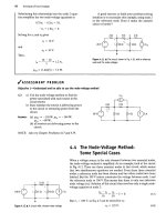
214 Response
of
First-Order
RL
and
RC
Circuits
R
eq
C,
eq.
(a)
(b)
Figure 7.1 • The two forms of the circuits for natural
response, (a)
RL
circuit, (b)
RC
circuit.
R
rii
L i v
(b)
(d)
Figure 7.2 A Four possible first-order circuits.
(a) An inductor connected to a Thevem'n equivalent.
(b) An inductor connected
to a
Norton equivalent.
(c) A capacitor connected to a Thevem'n equivalent.
(d) A capacitor connected to a Norton equivalent.
^V
r
= ()
Ro
Rkv
Figure 7.3 • An
RL
circuit.
/(0) = I \
L RZv
appear, if it can be reduced to a Thevenin or Norton equivalent connected
to the terminals of an equivalent inductor or capacitor, it is a first-order
circuit. (Note that if multiple inductors or capacitors exist in the original
circuit, they must be interconnected so that they can be replaced by a sin-
gle equivalent element.)
After introducing the techniques for analyzing the natural and step
responses of first-order circuits, we discuss some special cases of interest.
The first is that of sequential switching, involving circuits in which switching
can take place at two or more instants in time. Next is the unbounded
response. Finally, we analyze a useful circuit called the integrating amplifier.
7.1 The Natural Response
of an RL Circuit
The natural response of an RL circuit can best be described in terms of the
circuit shown in Fig. 7.3. We assume that the independent current source
generates a constant current of I
s
A, and that the switch has been in a
closed position for a long time. We define the phrase a long time more
accurately later in this section. For now it means that all currents and volt-
ages have reached a constant
value.
Thus only constant, or dc, currents can
exist in the circuit just prior to the switch's being opened, and therefore
the inductor appears as a short circuit (Ldi/dt = 0) prior to the release of
the stored energy.
Because the inductor appears as a short circuit, the voltage across the
inductive branch is zero, and there can be no current in either R
()
or R.
Therefore, all the source current /
s
appears in the inductive branch.
Finding the natural response requires finding the voltage and current at
the terminals of the resistor after the switch has been opened, that
is,
after
the source has been disconnected and the inductor begins releasing
energy. If we let t = 0 denote the instant when the switch is opened, the
problem becomes one of finding v(t) and i(t) for f>0. For t S 0, the cir-
cuit shown in Fig. 7.3 reduces to the one shown in Fig. 7.4.
Deriving the Expression for the Current
To find i(i), we use Kirchhoff s voltage law to obtain an expression involv-
ing i, R, and L. Summing the voltages around the closed loop gives
r dl
L—
+ Ri
dt
0,
(7.1)
where we use the passive sign convention. Equation 7.1 is known as a first-
order ordinary differential equation, because it contains terms involving
the ordinary derivative of the unknown, that is, di/dt. The highest order
derivative appearing in the equation is
1;
hence the term first-order.
We can go one step further in describing this equation. The coeffi-
cients in the equation, R and L, are constants; that is, they are not func-
tions of either the dependent variable i or the independent variable f.Thus
the equation can also be described as an ordinary differential equation
with constant coefficients.
To solve Eq.
7.1,
we divide by L, transpose the term involving i to the
right-hand side, and then multiply both sides by a differential time dt. The
result is
Figure 7.4 A The circuit shown in Fig. 7.3, for t s 0.
—dt= —-idt.
dt L
(7.2)
7.1 The Natural Response of
an RL
Circuit 215
Next, we recognize the left-hand side of Eq. 7.2 as a differential change in
the current /, that is, di. We now divide through by i, getting
di R
J
— =
—rdt.
i L
(7.3)
We obtain an explicit expression for i as a function of
f
by integrating both
sides of Eq.
7.3.
Using x and y as variables of integration yields
*(0
dx R
i(/„)
X U
<
(7.4)
in which /(f
0
) is the current corresponding to time fg, and /(f) is the current
corresponding to time f. Here, f
()
= 0. Therefore, carrying out the indi-
cated integration gives
/(f)
In
/(0)
R
=
~1
L
Based on the definition of the natural logarithm,
/(f) = i(0)e~
ls/L
K
(7.5)
(7.6)
Recall from Chapter 6 that an instantaneous change of current cannot
occur in an inductor. Therefore, in the first instant after the switch has
been opened, the current in the inductor remains unchanged. If we use 0~
to denote the time just prior to switching, and 0
+
for the time immediately
following switching, then
,(0-) = /(0
+
) = /
0
,
-4 Initial inductor current
where, as in Fig.
7.1,
/
()
denotes the initial current in the inductor. The initial
current in the inductor is oriented in the same direction as the reference
direction of
/.
Hence Eq. 7.6 becomes
/(f) = /
0
<T
WL)
', f ^ 0,
(7.7) -4 Natural response of an RL circuit
which shows that the current starts from an initial value I
()
and decreases
exponentially toward zero as f increases. Figure 7.5 shows this response.
We derive the voltage across the resistor in
Fig.
7.4 from a direct appli-
cation of Ohm's law:
v = iR = I
0
Re-
WL)t
, t > 0
+
. (7.8)
Note that in contrast to the expression for the current shown in Eq. 7.7,
the voltage is defined only for t > 0, not at f = 0. The reason is that a step
change occurs in the voltage at zero. Note that for t < 0, the derivative of
the current is zero, so the voltage is also zero. (This result follows from
v = Ldi/dt = 0.) Thus
?;(CT) = 0,
v(0
+
) = I
0
R,
(7.9)
(7.10)
where v(0
+
) is obtained from Eq. 7.8 with f =
0"
1
".
1
With this step change at
an instant in time, the value of the voltage at f = 0 is unknown. Thus we
use f > 0
+
in defining the region of validity for these solutions.
Figure 7.5 A
The
current response for the circuit shown
in
Fig.
7.4.
1
We can define the expressions
()""
and u
+
more formally. The expression x(0~) refers to the
limit of the variable x as / —»0 from the left, or from negative time. The expression .v(O')
refers to the limit of the variable x as /
—*•
0 from the right, or from positive time.