Electric Circuits, 9th Edition P27 potx
Bạn đang xem bản rút gọn của tài liệu. Xem và tải ngay bản đầy đủ của tài liệu tại đây (304.07 KB, 10 trang )
236 Response of First-Order
RL
and
RC
Circuits
no energy is stored in the circuit at the instant
the switch is closed.
Next we observe v
o
(0
+
) = 120 V, which is
consistent with the fact that i
o
(0) = 0.
Now we observe the solutions for ^ and
i
2
are consistent with the solution for v
0
by
observing
dii di
2
v
a
= 3— + 6—
dt dt
= 360*T
5
' - 240<T
5
'
= 120«?-* V, t > 0
+
,
or
dt dt
= 720e~
5
' - 600e
_5/
= 120e"
5
' V, t > 0
+
.
The final values of i\ and /
2
can be checked
using flux linkages. The flux linking the 3 H coil
(Aj) must be equal to the flux linking the 15 H
coil (A
2
), because
v„ =
Now
and
rfAj
~dt
dki
dt'
A, = 3ij + 6/
2
Wb-turns
A
2
= 6i] + 15/
2
Wb-turns.
Regardless of which expression we use, we
obtain
A, = A
2
= 24 - 24<T
5
' Wb-turns.
Note the solution for A
t
or A
2
is consistent with
the solution for v
D
.
The final value of the flux linking either
coil 1 or coil 2 is 24 Wb-turns, that is,
A
t
(oo) = A
2
(oo) = 24 Wb-turns.
The final value of
iy
is
^(oo) = 24 A
and the final value of i
2
is
/
2
(oo) = -8 A.
The consistency between these final values
for jj and i
2
and the final value of the flux link-
age can be seen from the expressions:
A^oo) = 3/2(00) + 6/
2
(oo)
= 3(24) + 6(-8) = 24 Wb-turns,
A
2
(oo) = 6^(00) + 15/
2
(oo)
= 6(24) + 15(-8) = 24 Wb-turns.
It is worth noting that the final values of ij
and /
2
can only be checked via flux linkage
because at t — 00 the two coils are ideal short
circuits. The division of current between ideal
short circuits cannot be found from Ohm's law.
NOTE: Assess your understanding of this material by using the general solution method to solve Chapter
Problems 7.68 and 7.69.
7.5 Sequential Switching
Whenever switching occurs more than once in a circuit, we have sequential
switching. For example, a single, two-position switch may be switched back
and forth, or multiple switches may be opened or closed in sequence. The
time reference for all switchings cannot be f = 0. We determine the volt-
ages and currents generated by a switching sequence by using the tech-
niques described previously in this chapter. We derive the expressions for
v(t) and i(t) for a given position of the switch or switches and then use
these solutions to determine the initial conditions for the next position of
the switch or switches.
With sequential switching problems, a premium is placed on obtaining
the initial value
x(t
0
).
Recall that anything but inductive currents and
capacitive voltages can change instantaneously at the time of switching.
Thus solving first for inductive currents and capacitive voltages is even
more pertinent in sequential switching problems. Drawing the circuit that
pertains to each time interval in such a problem is often helpful in the
solution process.
7.5 Sequential Switching 237
Examples 7.11 and 7.12 illustrate the analysis techniques for circuits
with sequential switching. The first is a natural response problem with two
switching times, and the second is a step response problem.
Example 7.11 Analyzing an
RL
Circuit that has Sequential Switching
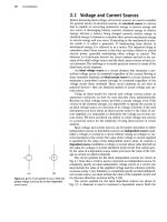
The two switches in the circuit shown in Fig. 7.31
have been closed for a long time. At t - 0, switch 1
is opened. Then, 35 ms later, switch 2 is opened.
a) Find i
L
{t) for 0 < t < 35 ms.
b) Find i
L
for t a 35 ms.
c) What percentage of the initial energy stored in
the 150 mH inductor is dissipated in the 18 ft
resistor?
d) Repeat (c) for the 3 17 resistor.
e) Repeat (c) for the 6
D,
resistor.
t = 0
t
=
35 ms
4H
KVr^fr^—
60 V
£12
(1
£6(1 <M
150
mH $18(1
Figure 7.31 •
The
circuit for Example 7.11.
Solution
a) For t < 0 both switches are closed, causing the
150 mH inductor to short-circuit the 18
D,
resis-
tor. The equivalent circuit is shown in
Fig.
7.32. We
determine the initial current in the inductor by
solving for ii£0~) in the circuit shown in Fig. 7.32.
After making several source transformations, we
find
i
L
(0~)
to be
6
A. For 0 < t < 35 ms, switch 1
is open (switch 2 is closed), which disconnects the
60 V voltage source and the 4 H and 12 £l resis-
tors from the circuit. The inductor is no longer
behaving as a short circuit (because the dc source
is no longer in the circuit), so the 18 O resistor is
no longer short-circuited. The equivalent circuit is
shown in Fig.
7.33.
Note that the equivalent resist-
ance across the terminals of the inductor is the
parallel combination of 9 O and 18 0, or 6 i\.
The time constant of the circuit is (150/6) X 10~
3
,
or 25
ms.
Therefore the expression for i
L
is
i
L
= 6e-
A{]l
A, 0 < t < 35 ms.
4(1
3(1
60
V
two")
Figure 7.32 • The circuit shown in Fig. 7.31, for t < 0.
Figure 7.33 • The circuit shown in Fig.
7.31,
for 0 < t ^35 ms.
b) When t = 35 ms, the value of the inductor
current is
i
L
= 6e~
u
= 1.48 A.
Thus,
when switch 2 is opened, the circuit
reduces to the one shown in Fig. 7.34, and the
time constant changes to (150/9) x 10
_
\ or
16.67 ms.The expression for i
L
becomes
i,=
1.486>-
6(,(
'-
a()35
>A,
t >35
ms.
Note that the exponential function is shifted in
time by 35 ms.
3(.
*'/.
6(1
v
L
] 150
mH
_? |i
L
{0.035)s 1.48 A
Figure 7.34 • The circuit shown in Fig. 7.31, for t > 35 ms.
c) The 18 n resistor is in the circuit only during the
first 35 ms of the switching sequence. During this
interval, the voltage across the resistor is
v, = 0.154(6<?"
40
')
dt
= -36e~
40
' V, 0 < t < 35 ms.
238 Response of First-Order
RL
and
RC
Circuits
The power dissipated in the 18 ft resistor is
p = -^ = 72<r
80
' W, 0 < t < 35 ms.
18
Hence the energy dissipated is
/.().035
W =
72<T
hl
V/
80/
.7(1
72
-SO/
0.035
0
-80
= 0.9(1 - ef
2
-
8
)
= 845.27 rnJ.
Tlie initial energy stored in the 150 mH inductor is
Wi = j(0.15)(36) = 2.7 J = 2700 mj.
Therefore (845.27/2700) x 100, or
31.31%
of
the initial energy stored in the 150 mH inductor
is dissipated in the 18 ft resistor.
d) For 0 < i < 35 ms, the voltage across the 3 ft
resistor is
*>m
»L
(3)
=
r
L
40/
Therefore the energy dissipated in the 3 ft resis-
tor in the first 35 ms is
.().035
WMl
"I44e
-SO/
dt
Jo 3
= 0.6(1 - e'
2
*)
= 563.51 mJ.
For t > 35 ms, the current in the 3 O resistor is
ha =
<L
=
(6e-^)e~W-^
A.
Hence the energy dissipated in the 3 ft resistor for
t > 35 ms is
t%i = I iiti X3dt
/().035
f 3(36)e-
2
*e-
ia
*-
tt,B5
>A
.7().035
108e
-
-
8
x
,-120(/-0.035)
120
0.035
108 _•)
o
_ . __,
—,»-
54.73mJ.
The total energy dissipated in the 3
("1
resistor is
w
3(l
(total) = 563.51 + 54.73
= 618.24 mJ.
The percentage of the initial energy stored is
618.24
2700
X 100 = 22.90%.
e) Because the 6 ft resistor is in series with the 3 12
resistor, the energy dissipated and the percent-
age of the initial energy stored will be twice that
of the 3 ft resistor:
w
6n
(total) = 1236.48 mJ,
and the percentage of the initial energy stored is
45.80%.
We check these calculations by observ-
ing that
1236.48 4- 618.24 + 845.27 = 2699.99 mJ
and
31.31 + 22.90 + 45.80 =
100.01%.
The small discrepancies in the summations are
the result of roundoff errors.
7.5 Sequential Switching
239
Example 7.12 Analyzing an
RC
Circuit that has Sequential Switching
The uncharged capacitor
in the
circuit shown
in
Fig. 7.35
is
initially switched
to
terminal
a of the
three-position switch. At
t
— 0, the switch is moved
to position b, where
it
remains for 15 ms. After the
15 ms delay, the switch is moved to position
c,
where
it remains indefinitely.
a) Derive the numerical expression for the voltage
across the capacitor.
b) Plot the capacitor voltage versus time.
c) When will
the
voltage
on the
capacitor equal
200 V?
Solution
a) At the instant the switch is moved to position b,
the initial voltage on the capacitor is zero.
If
the
switch were to remain in position b, the capacitor
would eventually charge to 400
V.
The time con-
stant of the circuit when the switch is in position
b
is
10
ms. Therefore
we can use
Eq. 7.59 with
t
()
= 0 to
write the expression
for
the capacitor
voltage:
v
=
400
+ (0 -
400)e
-100/
= (400 - 400e"
m
") V, 0 =s t < 15 ms.
Note that, because the switch remains
in
posi-
tion b for only 15 ms, this expression is valid only
for the time interval from
0 to
15 ms. After the
switch has been
in
this position
for
15 ms, the
voltage on the capacitor will be
y(15ms)
=
400
-
400e~
15
=
310.75 V.
Therefore, when the switch is moved to position c,
the initial voltage
on
the capacitor
is
310.75 V.
With the switch
in
position c, the final value of
the capacitor voltage
is
zero, and the time con-
stant is 5
ms.
Again, we use Eq. 7.59 to write the
expression for the capacitor voltage:
v
= 0 +
(310.75
-
())
e
-200(/-o.oi5)
= 310.75e-
20t)
('-
0()15
>V, 15ms
si/.
400 V(
) L v(t)^:0AfjLF
Figure 7.35
A
The circuit for Example 7.12.
In writing the expression
for
?;, we recognized
that
r<)
=
15 ms and that this expression
is
valid
only for
t ^
15 ms.
b) Figure 7.36 shows the plot of
v
versus
t.
c) The plot
in
Fig. 7.36 reveals that
the
capacitor
voltage will equal 200 V
at
two different times:
once
in the
interval between
0
and 15
ms
and
once after 15
ms.
We find the first time by solving
the expression
200
=
400
-
400<T
10,,
\
which yields
t\ =
6.93 ms. We find
the
second
time by solving the expression
200
=
310.756>-
2(,0(
';-°-
,),5)
.
In this case,
u =
17.20 ms.
v
= 4()0-4()0t'"
,m/
v =
3U).75e
2m
'
{m5)
t (ms)
Figure 7.36
•
The capacitor voltage for Example 7.12.
240 Response
of
First-Order
RL
and
RC
Circuits
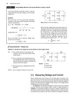
^ASSESSMENT PROBLEMS
Objective 3—Know how to analyze circuits with sequential switching
7.7
In the circuit shown, switch
1
has been closed
and switch 2 has been open for a long time. At
t = 0, switch
1
is opened. Then 10 ms later,
switch 2 is closed. Find
a) v
c
(t) for 0 < f < 0.01 s,
b) v
c
(t) for t > 0.01 s,
c) the total energy dissipated in the 25 kft
resistor, and
d) the total energy dissipated in the 100 kO
resistor.
(U
60kn
r=10m
" )10mAf40kft 25kft£lAtF
Answer: (a) 80e~
40/
V;
(b) 53.63e-
5
°('-
a01
W;
(c) 2.91 mJ;
(d) 0.29 mJ.
NOTE: Also try Chapter Problems 7.71 and 7.78.
7.8 Switch a in the circuit shown has been open for
a long time, and switch b has been closed for a
long time. Switch a is closed at t = 0 and, after
remaining closed for 1 s, is opened again.
Switch b is opened simultaneously, and both
switches remain open indefinitely. Determine
the expression for the inductor current i that is
valid when (a)0sf<h and (b) t > 1 s.
Answer: (a) (3 - 3e
_a5
') A, 0 < f < 1 s;
(b) (-4.8 + 5.98tf~
l
-
25(
'~
1>
) A, t > 1 s.
7.6 Unbounded Response
A circuit response may grow, rather than decay, exponentially with time.
This type of response, called an unbounded response, is possible if the cir-
cuit contains dependent sources. In that case, the Thevenin equivalent
resistance with respect to the terminals of either an inductor or a capacitor
may be negative. This negative resistance generates a negative time con-
stant, and the resulting currents and voltages increase without limit. In an
actual circuit, the response eventually reaches a limiting value when a
component breaks down or goes into a saturation state, prohibiting fur-
ther increases in voltage or current.
When we consider unbounded responses, the concept of a final value
is confusing. Hence, rather than using the step response solution given in
Eq. 7.59, we derive the differential equation that describes the circuit con-
taining the negative resistance and then solve it using the separation of
variables technique. Example 7.13 presents an exponentially growing
response in terms of the voltage across a capacitor.
7.7 The Integrating Amplifier 241
Example 7.13
Finding the Unbounded Response in an
RC
Circuit
a) When the switch is closed in the circuit shown in
Fig. 7.37, the voltage on the capacitor is 10 V.
Find the expression for v
a
for t > 0.
b) Assume that the capacitor short-circuits when
its terminal voltage reaches 150 V. How many
milliseconds elapse before the capacitor short-
circuits?
20 kn
Figure 7.37 • The circuit for Example 7.13.
Solution
a) To find the Thevenin equivalent resistance with
respect to the capacitor terminals, we use the test-
source method described in Chapter
4.
Figure 7.38
shows the resulting circuit, where v
r
is the test
voltage and i
T
is the test current. For Vj expressed
in
volts,
we obtain
ir = TT: ~ 7( ) +
—-
mA.
' 10 W 20
Solving for the ratio Vj/ir yields the Thevenin
resistance:
Km = — = -5 kn.
i
T
With this Thevenin resistance, we can simplify
the circuit shown in Fig. 7.37 to the one shown in
Fig. 7.39.
'T
Figure 7.38 • The test-source method used to find
i?
Th
.
-5kO
Figure 7.39 A A simplification of the circuit shown in
Fig.
7.37.
For t S: 0, the differential equation describing
the circuit shown in Fig. 7.39 is
(5 X 10
-6
)—^ - -r X 1()-
J
= 0.
dt 5
Dividing by the coefficient of the first derivative
yields
dv
0
dt
4(h>„ = 0.
We now use the separation of variables technique
to find v
(
,(t):
v
()
(t) = lOe
40
' V, t>0.
b) v
a
= 150 V when e
m
=
15.
Therefore, 40r = In 15,
and t = 67.70 ms.
NOTE: Assess your understanding of this material by trying Chapter Problems 7.85 and 7.87.
The fact that interconnected circuit elements may lead to ever-
increasing currents and voltages is important to engineers. If such inter-
connections are unintended, the resulting circuit may experience
unexpected, and potentially dangerous, component failures.
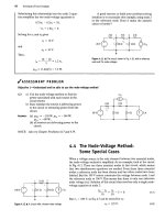
7.7 The Integrating Amplifier
Recall from the introduction to Chapter
5
that one reason for our interest in
the operational amplifier is its use as an integrating amplifier. We are now
ready to analyze an integrating-amplifier circuit, which is shown in
Fig.
7.40.
The purpose of such a circuit is to generate an output voltage proportional
to the integral of the input voltage. In Fig. 7.40, we added the branch cur-
rents if and /
v
, along with the node voltages v
n
and v
p
, to aid our analysis.
Figure 7.40 • An integrating amplifier.
242 Response of First-Order
RL
and
RC
Circuits
»i
K„ -
2f,
Figure 7.41 •
An
input voltage signal.
Figure 7.42 •
The
output voltage of
an
integrating
amplifier.
We assume that the operational amplifier is ideal. Thus we take
advantage of the constraints
Because v„ = 0,
if + i
s
= 0,
v
n
= v
p
.
i =^-
l
^^~dt
Hence, from Eqs. 7.61,7.63, and 7.64,
dv
a
_ 1
dt ~ R
s
C
f
v
s
.
(7.61)
(7.62)
(7.63)
(7.64)
(7.65)
Multiplying both sides of Eq. 7.65 by a differential time dt and then inte-
grating from f
()
to t generates the equation
Vo(0
\
R<C
v
s
dy + v
0
(t
()
). (7.66)
/•/A,
In Eq. 7.66,
t
()
represents the instant in time when we begin the integration.
Thus u„(?o) is the value of the output voltage at that time. Also, because
v
n
= v
p
=
0, v
o
(t
0
) is identical to the initial voltage on the feedback
capacitor C/.
Equation 7.66 states that the output voltage of an integrating ampli-
fier equals the initial value of the voltage on the capacitor plus an inverted
(minus sign), scaled (l/R
s
Cf) replica of the integral of the input voltage. If
no energy is stored in the capacitor when integration commences, Eq. 7.66
reduces to
vM = -
i
R
S
C
V
s
dy.
(7.67)
f A,
If v
s
is a step change in a dc voltage level, the output voltage will vary lin-
early with time. For example, assume that the input voltage is the rectan-
gular voltage pulse shown in Fig.
7.41.
Assume also that the initial value of
v
a
(t) is zero at the instant v
s
steps from 0 to V
m
. A direct application of
Eq. 7.66 yields
v„ =
1
V
m
t + 0, 0 < t < t
h
(7.68)
When t lies between t\ and 2t
u
1
v,
t
= -
#sQ Jt
{-V,
n
)dy
-
R
S
C,
V
m
h
RcCi
2V
m
R
x
c
t
t
h
t
L
< t < 2t
v
(7.69)
Figure 7.42 shows a sketch of v
(
,(t) versus t. Clearly, the output voltage is
an inverted, scaled replica of the integral of the input voltage.
The output voltage is proportional to the integral of the input voltage
only if the op amp operates within its linear range, that
is,
if it doesn't sat-
urate. Examples 7.14 and 7.15 further illustrate the analysis of the inte-
grating amplifier.
7.7 The Integrating Amplifier 243
Example 7.14
Analyzing an Integrating Amplifier
Assume that the numerical values for the signal
voltage shown in Fig. 7.41 are V
m
= 50 mV and
t\ = 1 s. This signal voltage is applied to the
integrating-amplifier circuit shown in Fig. 7.40. The
circuit parameters of the amplifier are R
s
= 100 kfl,
Cf = 0.1 ^iF, and Vcc = 6 V. The initial voltage on
the capacitor is zero.
a) Calculate v
a
(t).
b) Plot v
()
(t) versus t.
Solution
a) For 0 < t < 1 s,
-1
" (100 X 10
3
)(0.1 x 10"
6
)
= St V, 0 < f <
1
s.
50 X 10~
3
f + 0
For
1
< t < 2 s,
v
<t
= (5r - 10) V.
b) Figure 7.43 shows a plot of v„(t) versus r.
»„(0(V)*
2 t{t)
Figure 7.43 • The output voltage for Example 7.14.
Example 7.15
Analyzing an Integrating Amplifier that has Sequential Switching
At the instant the switch makes contact with termi-
nal a in the circuit shown in Fig. 7.44, the voltage on
the 0.1
/AF
capacitor is 5 V. The switch remains at
terminal a for 9 ms and then moves instantaneously
to terminal b. How many milliseconds after making
contact with terminal b does the operational ampli-
fier saturate?
Figure 7.44 • The circuit for Example 7.15.
Solution
The expression for the output voltage during the
time the switch is at terminal a is
1
io-
2
7o
= (-5 + 10000
v
(-10)^
Thus,
9 ms after the switch makes contact with ter-
minal a, the output voltage is -5 + 9, or 4 V.
The expression for the output voltage after the
switch moves to terminal b is
&dy
10"
2
9X
1()-
= 4 - 800(t - 9 X 10"
3
)
= (11.2 - 8000 V.
During this time interval, the voltage is decreas-
ing, and the operational amplifier eventually satu-
rates at
—6
V. Therefore we set the expression for v
a
equal to —6 V to obtain the saturation time t
s
:
11.2 - 800/, = -6,
or
t
s
= 21.5 ms.
Thus the integrating amplifier saturates 21.5 ms
after making contact with terminal b.
244 Response
of
First-Order
RL
and
RC
Circuits
From the examples, we see that the integrating amplifier can perform
the integration function very well, but only within specified limits that
avoid saturating the op amp. The op amp saturates due to the accumula-
tion of charge on the feedback capacitor. We can prevent it from saturat-
ing by placing a resistor in parallel with the feedback capacitor. We
examine such a circuit in Chapter 8.
Note that we can convert the integrating amplifier to a differentiating
amplifier by interchanging the input resistance R
s
and the feedback capac-
itor Cf. Then
v
a
= -R
S
C,
~dt
(7.70)
We leave the derivation of Eq. 7.70 as an exercise for you. The differentiat-
ing amplifier is seldom used because in practice it is a source of unwanted
or noisy signals.
Finally, we can design both integrating- and differentiating-amplifier
circuits by using an inductor instead of a capacitor. However, fabricating
capacitors for integrated-circuit devices is much easier, so inductors are
rarely used in integrating amplifiers.
^ASSESSMENT PROBLEMS
Objective 4—Be able to analyze op amp circuits containing resistors and a single capacitor
7.9 There is no energy stored in the capacitor at
the time the switch in the circuit makes contact
with terminal a. The switch remains at position
a for 32 ms and then moves instantaneously to
position b. How many milliseconds after mak-
ing contact with terminal a does the op amp
saturate?
7.10 a) When the switch closes in the circuit
shown, there is no energy stored in the
capacitor. How long does it take to saturate
the op amp?
b) Repeat (a) with an initial voltage on the
capacitor of
1 V,
positive at the upper
terminal.
40
m
10
kO
-AW
40 kn
/VW
v„
£ 6.8
kO,
Answer: 262 ms.
NOTE: Also try Chapter Problems 7.95 and 7.96.
Answer: (a) 1.11 ms;
(b) 1.76 ms.
Practical Perspective 245
Practical Perspective
A Flashing Light Circuit
We are now ready to analyze the flashing light circuit introduced at the
start of this chapter and shown in Fig. 7.45. The lamp in this circuit
starts to conduct whenever the lamp voltage reaches a value
V
max
.
During
the time the lamp conducts, it can be modeled as a resistor whose resist-
ance is R
L
. The lamp will continue to conduct until the lamp voltage
drops to the value V^
lin
. When the lamp is not conducting, it behaves as
an open circuit.
Before we develop the analytical expressions that describe the behav-
ior of the circuit, let us develop a feel for how the circuit works by noting
the following. First, when the lamp behaves as an open circuit, the dc
voltage source will charge the capacitor via the resistor R toward a value
of V
s
volts. However, once the lamp voltage reaches
V
max
,
it starts
con-
ducting and the capacitor will start to discharge toward the Thevenin
voltage seen from the terminals of the capacitor. But once the capacitor
voltage reaches the cutoff voltage of the lamp (V
min
), the lamp will act as
an open circuit and the capacitor will start to recharge. This cycle of
charging and discharging the capacitor is summarized in the sketch shown
in Fig. 7.46.
In drawing Fig. 7.46 we have chosen t = 0 at the instant the capacitor
starts to charge. The time t
0
represents the instant the lamp starts to
con-
duct, and t
c
is the end of a complete cycle. We should also mention that in
constructing Fig. 7.46 we have assumed the circuit has reached the repeti-
tive stage of its operation. Our design of the flashing light circuit requires
we develop the equation for Vjjj) as a function of V^ax, Vj^^, V
s
, R, C, and
R
L
for the intervals 0 to t
0
and t
Q
to f
c
.
To begin the analysis, we assume that the circuit has been in operation
for a long time. Let t = 0 at the instant when the lamp stops conducting.
Thus,
at t = 0, the lamp is modeled as an open circuit, and the voltage drop
across the lamp is V^
in
, as shown in Fig. 7.47.
From the circuit, we find
vd°°)
=
V
s
,
t>i,(0) =
v
min
,
T = RC.
R
->VvV
V.
c:
v
L
Lamp
Figure 7.45 A
A
flashing light circuit.
V
L{t)
y
v
max
V •
etc.
Figure 7.46 • Lamp voltage versus time for the
circuit in Fig. 7.45.
+
R
4-
v
L
Figure 7.47 A
The
flashing light circuit at t = 0,
when the lamp is not conducting.
Thus,
when the lamp is not conducting,
V
L
(t) = Vs + (Knin ~
V
s
)e-'S
RC
.
How long does it take before the lamp is ready to conduct? We can find this
time by setting the expression for v
L
(t) equal to
V
max
and solving for t. If
we call this value t
0
, then
t
n
= RC In
V • - V
y
min
v
s
V
—
V
K
max
y
s
When the lamp begins conducting, it can be modeled as a resistance R
L
,
as seen in Fig. 7.48. In order to find the expression for the voltage drop
+
T
R
C^
+
^v
L
1
R,
Figure 7.48 •
The
flashing light circuit at t = t
0
when the lamp is conducting.