Electric Circuits, 9th Edition P51 docx
Bạn đang xem bản rút gọn của tài liệu. Xem và tải ngay bản đầy đủ của tài liệu tại đây (278.47 KB, 10 trang )
476 The Laplace Transform in Circuit Analysis
where
co
= 40,000, a = 32,000, and
(3
= 24,000.
We can't test the final value of i
L
with the final-value theorem because
l
L
has a pair of poles on the imaginary axis; that is, poles at ±/4 X 10
4
.
Thus we must first find i
L
and then check the validity of the expression
from known circuit behavior.
When we expand Eq. 13.36 into a sum of partial fractions, we generate
the equation
/, =
K:
+
Kl
+
K,
s -/40,000 s + /40,000 s + 32,000 - /24,000
+
K\
s + 32,000 + /24,000
The numerical values of the coefficients K\ and K
2
are
384 X 10
5
(/40,000)
(13.37)
*1 = 7T
(/80,000)(32,000 + /16,000)(32,000 + /64,000)
= 7.5 X 10~
3
/-90°, (13.38)
K, =
384 X 10
5
( -32,000 + /24,000)
(-32,000 - /16,000)(-32,000 + /64,000)(/48,000)
12.5 X 10~
3
/90°. (13.39)
Substituting the numerical values from Eqs. 13.38 and 13.39 into
Eq. 13.37 and inverse-transforming the resulting expression yields
i
L
= [15 cos (40,000r - 90°)
+ 25e
-32.000?
cos(24,000r + 90°)] mA,
= (15 sin 40,000r - 2Se~
nmt
sin 24,000/)tt(0 mA. (13.40)
We now test Eq. 13.40 to see whether it makes sense in terms of the
given initial conditions and the known circuit behavior after the switch has
been open for a long time. For t = 0, Eq. 13.40 predicts zero initial current,
which agrees with the initial energy of zero in the circuit. Equation 13.40
also predicts a steady-state current of
i
La
= 15sin40,000rmA,
which can be verified by the phasor method (Chapter 9).
(13.41)
Figure 13.15 • A multiple-mesh
RL
circuit.
The Step Response of a Multiple Mesh Circuit
Until now, we avoided circuits that required two or more node-voltage or
48 ft mesh-current equations, because the techniques for solving simultaneous
differential equations are beyond the scope of this text. However, using
Laplace techniques, we can solve a problem like the one posed by the
multiple-mesh circuit in Fig. 13.15.
13.3 Applications 477
Here we want to find the branch currents /j and i
2
that arise when the
336 V dc voltage source is applied suddenly to the circuit. The initial
energy stored in the circuit is zero. Figure 13.16 shows the .v-domain equiv-
alent circuit of Fig.
13.15.
The two mesh-current equations are
336
= (42 +
8.45)/]
- 42/
2
,
0 = -42/j + (90 +
10s)I
2
.
Using Cramer's method to solve for l
x
and I
2
, we obtain
A =
42 + 8.4s - 42
- 42 90 + 10s
(13.42)
(13.43)
48 a
Figure 13.16 •
The
s-domain
equivalent circuit for the
circuit
shown
in Fig. 13.15.
=
84(5
2
+ 14.9 + 24)
= 84( s + 2)(5 + 12), (13.44)
A',
336/5 - 42
0 90 + 105
3360(5 + 9)
(13.45)
No =
42 + 8.45 336/5
- 42 0
14,112
(13.46)
Based on Eqs. 13.44-13.46,
/>
=
/Vi _ 40(5 + 9)
A " s(s + 2)(5 + 12)'
(13.47)
A =
N;
168
A 5(5 + 2)(5 + 12)'
Expanding I] and /
2
into a sum of partial fractions gives
14
1
15
5 5 + 2 5 + 12'
(13.48)
(13.49)
8.4 1.4
+
5 5 + 2 5+12
(13.50)
478 The Laplace Transform in Circuit Analysis
We obtain the expressions tor i
{
and i
2
by inverse-transforming Eqs. 13.49
and 13.50, respectively:
I, = (15 - Ue~
2t
- e~
]2t
)u(t) A, (13.51)
/
2
= (7 - 8.4e"
z
' + \Ae~
l
*)u(t) A.
(13.52)
Next we test the solutions to see whether they make sense in terms of the
circuit. Because no energy is stored in the circuit at the instant the switch is
closed, both /'i(0~) and /2(0
-
) must be zero. The solutions agree with these
initial
values.
After the switch has been closed for a long
time,
the two induc-
tors appear as short
circuits.
Therefore, the final values of i
{
and i
2
are
,
x
336(90)
/(00) = *—'- = 15 A,
1V )
42(48)
(13.53)
15(42)
/
2
(oo)=^ = 7A. (13.54)
One final test involves the numerical values of the exponents and calcu-
lating the voltage drop across the 42 11 resistor by three different methods.
From the circuit, the voltage across the 42 Q resistor (positive at the top) is
dii d'h
v = 42(/, - h) = 336 - 8.4—- = 48/, + 10-
2
dt dt
(13.55)
/'ASSESSMENT
PROBLEM
You should verify that regardless of which form of Eq. 13.55 is used, the
voltage is
v = (336 - 235.2e~
2r
- 100.80e"
12r
)«(0 V.
We are thus confident that the solutions for i
x
and i
2
are correct.
Objective
2—Know
how to analyze a circuit in the s domain and be able to transform an s domain solution to the
time domain
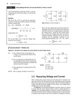
13.5 The dc current and voltage sources are
applied simultaneously to the circuit shown.
No energy is stored in the circuit at the instant
of application.
a) Derive the 5-domain expressions for V\
and V
2
.
b) For t > 0, derive the time-domain expres-
sions for
V\
and v
2
.
c) Calculate ^(0+) and v
2
(0
+
).
d) Compute the steady-state values of V\
and Vi.
Answer: (a) V
l
= [5(s + 3)]/[s(s + 0.5)(5 + 2)],
V
2
= [2.5(s
2
+ 6)]/[s(s + 0.5)(5 + 2)];
(b) v, = (15
50 -0.5/
+ f<r
2
>(0 v,
v
2
= 05 -
l
-fe-°-
51
+ ?e*)«(0 V;
(c) u,(0
+
) = 0, v
2
(0
+
) = 2.5 V;
(d) vi = v
2
= 15 V.
f>A <Z IF:
1H
_/-WY-\_
+
v\ 3 n f
v-
15a
15VI
NOTE: Also try Chapter Problems 13.22 and 13.29.
13.3 Applications 479
The Use of Thevenin's Equivalent
In this section we show how to use Thevenin's equivalent in the s domain.
Figure 13.17 shows the circuit to be analyzed. The problem is to find the
capacitor current that results from closing the switch.The energy stored in
the circuit prior to closing is zero.
To find i
c
, we first construct the 5-domain equivalent circuit and then
find the Thevenin equivalent of this circuit with respect to the terminals of
the capacitor. Figure 13.18 shows the 5-domain circuit.
The Thevenin voltage is the open-circuit voltage across terminals a, b.
Under open-circuit conditions, there is no voltage across the 60 Q resis-
tor. Hence
VTI,=
{480/s)(0.002s)
20 + 0.002*
480
5 + 10
4
'
(13.56)
The Thevenin impedance seen from terminals a and b equals the 60 ft
resistor in series with the parallel combination of the 20 fl resistor and the
2 mH inductor. Thus
Z
Th
= 60 +
0.0025(20) 80(5 + 7500)
20 + 0.0025
.v + KV
(13.57)
Using the Thevenin equivalent, we reduce the circuit shown in Fig. 13.18
to the one shown in Fig. 13.19. It indicates that the capacitor current I
c
equals the Thevenin voltage divided by the total series impedance. Thus,
Ir =
480/(5 + 10
4
)
[80(5 + 7500)/(5 + 10
4
)] + [(2 X 10
5
)/5]
We simplify Eq. 13.58 to
/c =
65
6.v
5
2
+ 10,0005 + 25 X 10
6
(s + 5000)
2
A partial fraction expansion of Eq. 13.59 generates
Ir =
-30,000
+
(5 + 5000)'
the inverse transform of which is
5 + 5000'
i
c
= (-30,000f«T
50,M)
' + 6e-
5m
')u(t) A.
(13.58)
(13.59)
(13.60)
(13.61)
We now test Eq. 13.61 to see whether it makes sense in terms of
known circuit behavior. From Eq.
13.61,
/
c
(0) = 6 A.
(13.62)
This result agrees with the initial current in the capacitor, as calculated from
the circuit in Fig. 13.17. The initial inductor current is zero and the initial
capacitor voltage is zero, so the initial capacitor current is 480/80, or 6 A.
The final value of the current is zero, which also agrees with Eq.
13.61.
Note
also from this equation that the current reverses sign when t exceeds
6/30.000, or 200
/AS.
The fact that ic reverses sign makes sense because,
when the switch first closes, the capacitor begins to charge. Eventually this
charge is reduced to zero because the inductor is a short circuit at t = co.
The sign reversal of i
c
reflects the charging and discharging of the capacitor.
Let's assume that the voltage drop across the capacitor v
c
is also of inter-
est. Once we know i
c
. we find v
c
by integration in the time domain; that is,
v
c
= 2 x 10
5
/(6- 30,
-5(K«h
0Q0x)e~^
m,x
dx.
(13.63)
20 fi
60
a
a
'VW-
Figure 13.17 A A circuit to be analyzed using
Thevenin's equivalent in the s domain.
20 O
60
0 a
-^vw •-
N4
|^
10.002
s V
c
/c
t
-±z2x 10
5
Figure 13.18 • The 5-domain model of the circuit
shown in Fig. 13.17.
v
c
i
c
;^2xio
5
Figure 13.19 • A simplified version of the circuit
shown in Fig. 13.18, using a Thevenin equivalent.
480 The Laplace Transform in Circuit Analysis
Although the integration called for in Eq. 13.63 is not difficult, we may
avoid it altogether by first finding the s-domain expression for V
c
and then
finding v
c
by an inverse transform. Thus
V
c
= -pic
sC
2 X 10
5
6.v
s (s + 5000)
2
from which
12 X 10
5
(s + 5000)^
v
c
= 12 x
io
5
rtr
50f)0
'u(0-
(13.64)
(13.65)
You should verify that Eq. 13.65 is consistent with Eq. 13.63 and that it
also supports the observations made with regard to the behavior of i
c
(see
Problem 13.33).
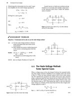
Objective 2—Know how to analyze a circuit in the s domain and be able to transform an s-domain solution to the
time domain
13.6 The initial charge on the capacitor in the circuit
shown is zero.
a) Find the 5-domain Thevenin equivalent cir-
cuit with respect to terminals a and b.
b) Find the s-domain expression for the current
that the circuit delivers to a load consisting of
a
1
H inductor in series with a 2 ft resistor.
Answer: (a) V
Th
= V
&h
= [20(5 + 2A))/[s(s + 2)),
Z
Ttl
= 5(5 + 2.8)/(s + 2);
NOTE: Also try Chapter Problem 13.34.
(b) J
ab
= [20(5 + 2A)]/[s(s + 3)(5 + 6)].
0.5 F
A Circuit with Mutual Inductance
The next example illustrates how to use the Laplace transform to analyze
the transient response of a circuit that contains mutual inductance.
Figure 13.20 shows the circuit. The make-before-break switch has been in
position a for a long time. At t = 0, the switch moves instantaneously to
position
b.
The problem is to derive the time-domain expression for i
2
.
We begin by redrawing the circuit in Fig. 13.20, with the switch in
position b and the magnetically coupled coils replaced with a T-equivalent
circuit.
1
Figure 13.21 shows the new circuit.
9fi
©
3
a
-'VW-
/ = 0
2H
2D,
^vw-
60 V
2H
8H
Figure 13.20 •
A
circuit containing magnetically coupled coils.
h ion
Sec Appendix C.
13.3 Applications 481
We now transform this circuit to the s domain. In so doing, we note that
fl(
°"
)=
f
= 5A
'
WO = 0.
(13.66)
(13.67)
Because we plan to use mesh analysis in the s domain, we use the series
equivalent circuit for an inductor carrying an initial current. Figure 13.22
shows the s-domain circuit. Note that there is only one independent volt-
age source. This source appears in the vertical leg of the tee to account for
the initial value of the current in the 2 H inductor of /,(0
-
) +
/
2
(0~),
or
5
A.
The branch carrying /, has no voltage source because L
t
- M = 0.
The two i'-domain mesh equations that describe the circuit in
Fig. 13.22 are
(3 + 2s)I
}
+ 2sl
2
= 10
2sT
t
+ (12 + 85)/
2
= 10.
Solving for /
2
yields
/2 =
2.5
(s + l)(j + 3)
Expanding Eq. 13.70 into a sum of partial fractions generates
1.25 1.25
/7 =
s + 1 s + 3
Then,
i
2
= (1.25e"' -
1.25e"
3/
)w(0
A.
(13.68)
(13.69)
(13.70)
(13.71)
(13.72)
Equation 13.72 reveals that i
2
increases from zero to a peak value of
481.13 mA in 549.31 ms after the switch is moved to position
b.
Thereafter,
/
2
decreases exponentially toward zero. Figure 13.23 shows a plot of i
2
ver-
sus
t.
This response makes sense in terms of the known physical behavior
of the magnetically coupled coils. A current can exist in the L
2
inductor
only if there is a time-varying current in the L, inductor. As i\ decreases
from its initial value of 5 A, /
2
increases from zero and then approaches
zero as i, approaches zero.
(L,
- M) (L
2
- M)
3H OH 6H 2ti
(MH2H
10
a
Figure 13.21 A The circuit shown in Fig. 13.20, with
the magnetically coupled coils replaced by
a
T-equivalent
circuit.
Figure 13.22 A The s-domain equivalent circuit for the
circuit shown in Fig.
13.21.
i
2
(mA)
481.13
549.31
/(ms)
Figure 13.23 A The plot of i
2
versus t for the circuit
shown in Fig. 13.20.
/ASSESSMENT PROBLEM
Objective 2—Know how to analyze a circuit in the s domain and be able to transform an s-domain solution to the
time domain
13.7 a) Verify from Eq. 13.72 that /
2
reaches a peak
value of 481.13 mA at t = 549.31 ms.
b) Find i
h
for t > 0, for the circuit shown in
Fig. 13.20.
c) Compute di
x
fdt when i
2
is at its peak value.
d) Express i
2
as a function of dii/dt when i
2
is
at its peak value.
e) Use the results obtained in (c) and (d) to
calculate the peak value of i
2
.
Answer: (a) di
2
/dt = 0 when t = |ln3 (s);
(b) /, = 2.5(6'"' + e"
3
>(0 A;
(c) -2.89 A/s;
(d) /
2
= -{MdiJdt)/\2\
(e) 481.13 mA.
NOTE: Also try Chapter Problems 13.39 and 13.40.
482
The
Laplace Transform
in
Circuit Analysis
+
y
Vj
< Ri
Figure
13.24 • A
circuit showing
the
use
of
super-
position
in
s-domain analysis.
Figure
13.25 •
The s-domain equivalent
for the
circuit
of
Fig.
13.24.
Figure
13.26 •
The circuit shown
in Fig. 13.25
with
V^
acting alone.
The
Use of
Superposition
Because
we are
analyzing linear lumped-parameter circuits,
we can use
superposition
to
divide
the
response into components that
can be
identi-
fied with particular sources
and
initial conditions. Distinguishing these
components
is
critical
to
being able
to use the
transfer function, which
we
introduce
in the
next section.
Figure
13.24
shows
our
illustrative circuit.
We
assume that
at the
instant when
the two
sources
are
applied
to the
circuit,
the
inductor
is
car-
rying
an
initial current
of p
amperes
and
that
the
capacitor
is
carrying
an
initial voltage
of y
volts. The desired response
of the
circuit
is the
voltage
across
the
resistor
R
2
,
labeled
v
2
.
Figure 13.25 shows
the
s-domain equivalent circuit. We opted
for the
parallel equivalents
for L and C
because
we
anticipated solving
for V
2
using
the
node-voltage method.
To find
V
2
by
superposition,
we
calculate
the
component
of V
2
result-
ing from each source acting alone,
and
then
we sum the
components.
We
begin with
V
g
acting alone. Opening each
of the
three current sources
deactivates them. Figure
13.26
shows
the
resulting circuit. We added
the
node voltage
V{ to aid the
analysis. The primes
on V
t
and V
2
indicate that
they
are the
components
of
Vj
and V
2
attributable
to V
g
acting alone.
The
two equations that describe
the
circuit
in
Fig. 13.26
are
J_
Ri
l
sL
V*
+
— + sC \V\ - sCV'
2
= -P-,
fli
\-jf
+ sC
(13.73)
(13.74)
For convenience,
we
introduce
the
notation
Y
»
=
i
+
i
+
sC
(13.75)
Y
l2
= sC;
(13.76)
K
22
= 4- + ^.
K
2
(13.77)
Substituting Eqs. 13.75-13.77 into Eqs. 13.73
and
13.74 gives
Y
n
V\ +
Y
n
V
2
= V
g
/R
h
(13.78)
Y„V\
+
YnV'r,
= 0.
12"
1
(13.79)
Solving Eqs. 13.78
and
13.79
for
V'
2
gives
V'o
^11¾
_
*12
(13.80)
With
the
current source
I
g
acting alone,
the
circuit shown
in
Fig.
13.25
reduces
to the one
shown
in Fig.
13.27. Here,
V'{ and V
2
are the
compo-
nents
of
V
x
and V
2
resulting from
L. If we use the
notation introduced
in
13.3 Applications
483
Eqs.
13.75-13.77,
the two
node-voltage equations that describe
the
circuit
in Fig. 13.27
are
Y
u
V"i
+
YnV'i
= 0
(13.81)
and
1/sC
-1(-
sLAV'[
V'^R,
Y
l2
Vl
+
Y
22
V'i
= I
r
Solving Eqs. 13.81
and
13.82
for V'i
yields
V'i
= ^-j-/
Ml'22
—
'12
Figure 13.27
•
The circuit shown
in
Fig. 13.25, with
(13.82)
j
g
acting alone.
(13.83)
To find the component
of V
2
resulting from the initial energy stored
in
the inductor {V%), we must solve
the
circuit shown
in
Fig. 13.28, where
Fi
9U"-e 13.28
•
The
circuit shown in Fig. 13.25, with
the energized inductor acting alone.
YnV'{'
+
Y
l2
V
2
"
= -p/s,
(13.84)
Y
12
Vf
+
Y
22
V'{
= 0.
Til us
V'i'
=
Yjs
Ml*22
-yl
V-
* 12
(13.85)
(13.86)
From
the
circuit shown
in Fig.
13.29,
we
find
the
component
of
V
2
iy'i') resulting from
the
initial energy stored
in the
capacitor.
The
node-voltage equations describing this circuit
are
YuVT
+
Y
l2
V?
= yC,
K„Vr
+
Yy>V7
= -yC.
22^
2
Solving
for
Vf
yields
Y\\Y
2
2
Yyi
The expression
for V
2
is
V
2
=V'
2
+ V'i + V'i' +
V'i"
(13.87)
(13.88)
(13.89)
Figure 13.29
A
The circuit shown
in
Fig. 13.25, with
the energized capacitor acting alone.
-(Yn/Ri)
Y\\Y
22
- Y\\
*i +
—
—
7
.?
Y\]Y
22
- Yyi
+
Y
]2
/s
Y]\Y
22
Y\
2
-C(Y
U
+ Y
n
)
p
^ T~
y-
Y\\Y
22
— Y i2
(13.90)
We
can
find
V
2
without using superposition
by
solving
the
two node-
voltage equations that describe the circuit shown
in
Fig.
13.25.
Thus
484 The Laplace Transform
in
Circuit Analysis
(13.91)
Y
X2
V
X
+ Y
22
V
2
= I - yC.
(13.92)
You should verify
in
Problem 13.43 that
the
solution
of
Eqs. 13.91
and
13.92 for V
2
gives the same result as Eq. 13.90.
•ASSESSMENT PROBLEM
Objective 2—Know how to analyze
a
circuit in the s domain and be able to transform an s-domain solution
to
the
time domain
13.8 The energy stored in the circuit shown is zero
at the instant the two sources are turned on.
a) Find the component
of v
for
t > 0
owing
to
the voltage source.
b) Find the component
of v
for
t > 0
owing
to
the current source.
c) Find the expression for
v
when
t > 0.
NOTE: Also try Chapter Problem 13.42.
Answer:
(a)
[(100/3)e"
2
'
-
(100/3)<T
8r
jw(0
V;
(b) [(50/3)<T
2
'
-
(50/3)e-*')u(t)
V;
(c) [50<T
2
'
-
50e"
8
']«(0
V.
2fl
20u(t)f +
1.25IH
»
:50mF(t ^
5u{t)
13.4 The Transfer Function
The transfer function is defined as the s-domain ratio of the Laplace trans-
form
of the
output (response)
to the
Laplace transform
of the
input
(source).
In
computing the transfer function, we restrict
our
attention
to
circuits where all initial conditions are zero.
If a
circuit has multiple inde-
pendent sources, we can find the transfer function for each source and use
superposition to find the response to all sources.
The transfer function
is
Definition
of
a transfer function
•
H(s)
=
Y(s)
X(s)'
(13.93)
sL
\/sC
Figure 13.30
•
A series
RLC
circuit.
where
Y(s) is
the Laplace transform
of
the output signal, and
X(s) is the
Laplace transform
of the
input signal. Note that
the
transfer function
depends
on
what
is
defined
as the
output signal. Consider,
for
example,
the series circuit shown
in
Fig. 13.30.
If the
current
is
defined
as the
response signal
of
the circuit,
H(s)
=
1
sC
]_
__
V~R
+ sL+ 1/sC ~
S
2
LC
+ RCs + 1
(13.94)
In deriving Eq. 13.94, we recognized that /corresponds to the output
Y(s)
and V
g
corresponds
to
the input
X(s).
13.4 The Transfer Function
485
If the voltage across the capacitor is defined as the output signal of the
circuit shown in Fig. 13.30, the transfer function is
H(s) =
V
1/sC
1
R + sL + 1/sC s
2
LC + RCs + 1
(13.95)
Thus,
because circuits may have multiple sources and because the definition
of the output signal of interest can vary, a single circuit can generate many
transfer functions. Remember that when multiple sources are involved, no
single transfer function can represent the total output—transfer functions
associated with each source must be combined using superposition to yield
the total response. Example 13.1 illustrates the computation of a transfer
function for known numerical values of R, L, and C.
Example 13.1
Deriving the Transfer Function of a Circuit
The voltage source v„ drives the circuit shown in
Fig.
13.31.
The response signal is the voltage across
the capacitor,
v
(>
.
a) Calculate the numerical expression for the trans-
fer function.
b) Calculate the numerical values for the poles and
zeros of the transfer function.
1000
a
AM,
250fi
50 mH
+
1 ju.F
v
t>
Figure 13.31 A
The
circuit for Example 13.1.
Solution
a) The first step in finding the transfer function is to
construct the 5-domain equivalent circuit, as
shown in Fig. 13.32. By definition, the transfer
function is the ratio of
V
0
/V
s
,
which can be com-
puted from a single node-voltage equation.
Summing the currents away from the upper
node generates
V - V
<>
.?
1000
+
V'
V„s
250 + 0.055 10
6
= 0.
ooo
n
AM-—
s
Figure 13.32 •
The
s-domain equivalent circuit for the circuit
shown in Fig.
13.31.
Solving for
V
()
yields
1000(5 + 5()00)¾
Vo =
5
2
+ 60005 + 25 X 10
6
'
Hence the transfer function is
s
1000(5 + 5000)
" 5
2
+ 60005 + 25 X 10
6
"
b) The poles of H{s) are the roots of the denomina-
tor polynomial. Therefore
-p
]
= -3000 - y'4000,
-p
2
= -3000 + /4000.
The zeros of H(s) are the roots of the numera-
tor polynomial; thus H(s) has a zero at
-Zi = -5000.