Electric Circuits, 9th Edition P58 potx
Bạn đang xem bản rút gọn của tài liệu. Xem và tải ngay bản đầy đủ của tài liệu tại đây (792.57 KB, 10 trang )
546 Introduction to Frequency Selective Circuits
R
,6
<\>
C
(c)
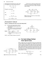
Figure 14.28 • (a) A series
RLC
bandreject filter.
(b) The equivalent circuit for
00
= 0. (c) The equivalent
circuit for
co
= 00.
\ff(h*)\
90° -
Figure 14.29 • The frequency response plot for the
series
RLC
bandreject filter circuit in Fig. 14.28(a).
before they reach the output at frequencies between the two cutoff fre-
quencies (the stopband). Bandpass filters and bandreject filters thus per-
form complementary functions in the frequency domain.
Bandreject filters are characterized by the same parameters as band-
pass filters: the two cutoff frequencies, the center frequency, the band-
width, and the quality factor. Again, only two of these five parameters can
be specified independently.
In the next sections, we examine two circuits that function as band-
reject filters and then compute equations that relate the circuit compo-
nent values to the characteristic parameters for each circuit.
The Series
RLC
Circuit—Qualitative Analysis
Figure 14.28(a) shows a series RLC circuit. Although the circuit components
and connections are identical to those in the series RLC bandpass filter in
Fig. 14.19(a), the circuit in Fig. 14.28(a) has an important difference: the out-
put voltage is now defined across the inductor-capacitor pair. As we saw in
the case of low- and high-pass filters, the same circuit may perform two
dif-
ferent filtering functions, depending on the definition of the output voltage.
We have already noted that at to = 0, the inductor behaves like a
short circuit and the capacitor behaves like an open circuit, but at
a) = 00, these roles switch. Figure 14.28(b) presents the equivalent cir-
cuit for
a)
= 0; Fig. 14.28(c) presents the equivalent circuit for
to
= 00. In
both equivalent circuits, the output voltage is defined over an effective
open circuit, and thus the output and input voltages have the same mag-
nitude. This series RLC bandreject filter circuit then has two pass-
bands—one below a lower cutoff frequency, and the other above an
upper cutoff frequency.
Between these two passbands, both the inductor and the capacitor
have finite impedances of opposite signs. As the frequency is increased
from zero, the impedance of the inductor increases and that of the capac-
itor decreases. Therefore the phase shift between the input and the out-
put approaches —90° as toL approaches
1/OJC.
AS soon as coL exceeds
1/wC, the phase shift jumps to +90° and then approaches zero as to con-
tinues to increase.
At some frequency between the two passbands, the impedances of the
inductor and capacitor are equal but of opposite sign. At this frequency,
the series combination of the inductor and capacitor is that of a short cir-
cuit, so the magnitude of the output voltage must be zero. This is the cen-
ter frequency of this series RLC bandreject filter.
Figure 14.29 presents a sketch of the frequency response of the series
RLC bandreject filter from Fig. 14.28(a). Note that the magnitude plot is
overlaid with that of the ideal bandreject filter from Fig. 14.3(d). Our qual-
itative analysis has confirmed the shape of the magnitude and phase angle
plots.
We now turn to a quantitative analysis of the circuit to confirm this
frequency response and to compute values for the parameters that charac-
terize this response.
^(•v)
Figure 14.30 • The s-domain equivalent of the circuit
in Fig. 14.28(a).
The Series
RLC
Circuit—Quantitative Analysis
After transforming to the s-domain, as shown in Fig. 14.30, we use voltage
division to construct an equation for the transfer function:
H(s) =
^Tc
R + sL + —
sC
s
2
+
1
LC
•>
R l
(14.43)
Substitute jco for 5 in Eq. 14.43 and generate equations for the transfer
function magnitude and the phase angle:
[H(jm)\
=
LC
LC
+
?)"
(14.44)
6(ja>)
=
—
tan
-1
wR
L
(14.45)
LC
Note that Eqs. 14.44 and 14.45 confirm the frequency response shape
pictured in Fig. 14.29, which we developed based on the qualita-
tive analysis.
Wc use the circuit in Fig. 14.30 to calculate the center frequency. For
the bandreject filter, the center frequency is still defined as the frequency
for which the sum of the impedances of the capacitor and inductor is zero.
In the bandpass filter, the magnitude at the center frequency was a maxi-
mum, but in the bandreject filter, this magnitude is a minimum. This is
because in the bandreject filter, the center frequency is not in the pass-
band; rather, it is in the stopband. It is easy to show that the center fre-
quency is given by
V
LC
(14.46)
Substituting Eq. 14.46 into Eq. 14.44 shows that \H(jco
0
)\ = 0.
The cutoff frequencies, the bandwidth, and the quality factor are
defined for the bandreject filter in exactly the way they were for the
bandpass filters. Compute the cutoff frequencies by substituting the
constant (l/V2)//
max
for the left-hand side of Eq. 14.44 and then solv-
ing for
co
cl
and w
c2
- Note that for the bandreject filter,
#max
=
1^(/0)1
= \H(j
oo)\,
and for the series RLC bandreject filter in
Fig. 14.28(a), H
BUX
= l.Thus,
0>c\ =
. -A
_,
. fJLY
2L
+
2LJ LC
(14.47)
R
^-
=
2L
+
R_
2L
+
LC
(14.48)
Use the cutoff frequencies to generate an expression for the band-
width, jS:
0 = R/L.
(14.49)
Finally, the center frequency and the bandwidth produce an equation for
the quality factor, Q:
Q =
R
2
C
(14.50)
548 Introduction to Frequency Selective Circuits
Again, we can represent the expressions for the two cutoff frequencies
in terms of the bandwidth and center frequency, as we did for the band-
pass filter:
cl
2
(14.51)
to*
+
+ cof
(14.52)
Alternative forms for these equations express the cutoff frequencies in
terms of the quality factor and the center frequency:
(0
ct
w
c2
= t0
o
'
¾
+
V
1
+
(¾)
k
+
V
1
+
Qa)\
i
(14.53)
(14.54)
Example 14.8 presents the design of a series RLC bandreject filter.
Example 14.8
Designing a Series
RLC
Bandreject Filter
Using the series RLC circuit in Fig. 14.28(a), com-
pute the component values that yield a bandreject
filter with a bandwidth of 250 Hz and a center fre-
quency of 750 Hz. Use a 100 nF capacitor. Compute
values for R, L, a)
ch
a>
c
.
2
, and Q.
Solution
We begin by using the definition of quality factor to
compute its value for this filter:
Q =
<oJ(3
= 3.
Use Eq. 14.46 to compute L, remembering to con-
vert io
a
to radians per second:
colC
[2TT(750)]
2
(100 X 10"
9
)
= 450 mH.
Use Eq. 14.49 to calculate R:
R = (3L
= 277(250)(450 x 10"
3
)
= 707 a
The values for the center frequency and band-
width can be used in Eqs. 14.51 and 14.52 to com-
pute the two cutoff frequencies:
co
c]
=
0
+
f
1
3992.0 rad/s,
0)
c2
P
+
PV
+ uf
= 5562.8 rad/s.
The cutoff frequencies are at 635.3 Hz and 885.3 Hz.
Their difference is 885.3 - 635.3 = 250 Hz, con-
firming the specified bandwidth. The geometric
mean is V(635.3)(885.3) = 750 Hz, confirming the
specified center frequency.
14.5 Bandreject Filters 549
As you might suspect by now, another configuration that produces a
bandreject filter is a parallel RLC circuit. Whereas the analysis details of
the parallel RLC circuit are left to Problem 14.34, the results are summa-
rized in Fig.
14.31,
along with the series RLC bandreject filter. As we did
for other categories of filters, we can state a general form for the transfer
functions of bandreject filters, replacing the constant terms with /3 and
OJ
(
;.
//(5)
s
2
+ d
s
z
+ jSs +
<a%
2'
(14.55) A Transfer function for
RLC
bandreject filter
Equation 14.55 is useful in filter design, because any circuit with a transfer
function in this form can be used as a bandreject filter.
H(s)=~2
s
2
+ l/LC
s
1
+ (R/L)s + l/LC
>
0
= VT/LC P = R/L
"•©
sL
sC
+
H(s) =
s
2
+ l/LC
s
2
+
s/RC + l/LC
co
0
= VljLC p = l/RC
Figure 14.31 • Two
RLC
bandreject filters, together
with equations for the transfer function, center
frequency, and bandwidth of each.
/ASSESSMENT PROBLEMS
Objective 4—Know the
RLC
circuit configurations that act as bandreject filters
14.10 Design the component values for the series
RLC bandreject filter shown in Fig. 14.28(a) so
that the center frequency is 4 kHz and the
quality factor is 5. Use a 500 nF capacitor.
Answer: L = 3.17 mH,
R = 15.92 H.
NOTE: Also try Chapter Problems 14.35 and 14.36.
14.11 Recompute the component values for
Assessment Problem 14.10 to achieve a band-
reject filter with a center frequency of 20 kHz.
The filter has a 100 fi resistor. The quality fac-
tor remains at 5.
Answer: L = 3.98 mH,
C = 15.92 nF.
550 Introduction to Frequency Selective Circuits
Practical Perspective
69?
**
770
#
%
8521» 1
941
H*
O '
Figure 14.32 • Tones generated by the rows and
columns of telephone pushbuttons.
Pushbutton Telephone Circuits
In the Practical Perspective at the start of this chapter, we described the
dual-tone-multiple-frequency (DTMF) system used to signal that a button
has been pushed on a pushbutton telephone. A key element of the DTMF
system is the DTMF receiver—a circuit that decodes the tones produced by
pushing a button and determines which button was pushed.
In order to design a DTMF reciever, we need a better understanding of
the DTMF system. As you can see from Fig. 14.32, the buttons on the tele-
phone are organized into rows and columns. The pair of tones generated by
pushing a button depends on the button's row and column. The button's row
determines its low-frequency tone, and the button's column determines its
high-frequency tone.
1
For example, pressing the "6" button produces
sinu-
soidal tones with the frequencies 770 Hz and 1477 Hz.
At the telephone switching facility, bandpass filters in the DTMF receiver
first detect whether tones from both the low-frequency and high-frequency
groups are simultaneously present. This test rejects many extraneous audio
signals that are not DTMF. If tones are present in both bands, other filters are
used to select among the possible tones in each band so that the frequencies
can be decoded into a unique button signal. Additional tests are performed to
prevent false button detection. For example, only one tone per frequency
band is allowed; the
high-
and low-band frequencies must start and stop
within a few milliseconds of one another to be considered
valid;
and the highl-
and low-band signal amplitudes must be sufficiently close to each other.
You may wonder why bandpass filters are used instead of a high-pass
filter for the high-frequency group of DTMF tones and a low-pass filter for
the low-frequency group of DTMF tones. The reason is that the telephone
system uses frequencies outside of the 300-3 kHz band for other signal-
ing purposes, such as ringing the phone's
bell.
Bandpass filters prevent
the DTMF receiver from erroneously detecting these other signals.
NOTE:
Assess
your understanding of this Practical Perspective by trying
Chapter Problems
14.46-14.48.
1
A fourth high-frequency tone is reserved at 1633 Hz. This tone is used infrequently and is not
produced by a standard 12-button telephone.
Summary
A frequency selective circuit, or
filter,
enables signals at
certain frequencies to reach the output, and it attenu-
ates signals at other frequencies to prevent them from
reaching the output. The passband contains the fre-
quencies of those signals that are passed; the stopband
contains the frequencies of those signals that are atten-
uated. (See page 524.)
The cutoff frequency, co
c
, identifies the location on the
frequency axis that separates the stopband from the
passband. At the cutoff frequency, the magnitude of the
transfer function equals (1/V2)//
raax
. (See page 527.)
A low-pass filter passes voltages at frequencies below
(a
c
and attenuates frequencies above
co
c
.
Any circuit
with the transfer function
/.>
H{s)
S + (o
c
functions as a low-pass filter. (See page 531.)
Problems 551
A high-pass filter passes voltages at frequencies above
and attenuates voltages at frequencies below Any cir-
cuit with the transfer function
H{s) = -
functions as a high-pass filter. (See page 536.)
Bandpass filters and bandreject filters each have two cut-
off frequencies,
a)
c]
and a;
c2
. These filters are further char-
acterized by their center frequency («„), bandwidth (/3),
and quality factor (Q). These quantities are defined as
w
0
= Vco
t
i
•
(o
c2
,
(3 = (o
c2
- o)
d
,
Q = "o/P.
(See pages 539-540.)
A bandpass filter passes voltages at frequencies within
the passband, which is between a>
cl
and
u)
c2
-
It attenuates
frequencies outside of the passband. Any circuit with the
transfer function
His)
Ps
r + Pi
functions as a bandpass filter. (See page 544.)
A bandreject filter attenuates voltages at frequencies
within the stopband, which is between
co
c]
and w
c2
. It
passes frequencies outside of the stopband. Any circuit
with the transfer function
His)
JT + (t)n
S
2
+ p
s
+ <4
functions as a bandreject filter. (See page 549.)
Adding a load to the output of a passive filter changes
its filtering properties by altering the location and mag-
nitude of the passband. Replacing an ideal voltage
source with one whose source resistance is nonzero also
changes the filtering properties of the rest of the circuit,
again by altering the location and magnitude of the
passband. (See page 542.)
Problems
Section 14.2
14.1 a) Find the cutoff frequency in hertz for the RL fil-
ter shown in Fig.
P14.1.
b)
Calculate
H(Jm) at
G>
C
,
0.2W
C
.,
and 5w
c
c) If Vj = lOcosatf V, write the steady-state
expression for v
a
when
co
= w
(
.,
co
= 0.2w
r
, and
a) = 5oo
c
.
Figure P14.1
10
mH
m
rv^r*r\
« m
127
a
14.2 Use a
1
mH inductor to design a low-pass, RL, pas-
OESIGN
s
ive filter with a cutoff frequency of
5
kHz.
PROBLEM
"
J
PSPICE
a
) Specify the value of the resistor.
MULTISIM
b) A load having a resistance of 68 fi is connected
across the output terminals of the filter. What is
the corner, or
cutoff,
frequency of the loaded fil-
ter in hertz?
c) If you must use a single resistor from Appendix H
for part (a), what resistor should you use? What is
the resulting cutoff frequency of the filter?
14.3 A resistor, denoted as R/, is added in series with the
inductor in the circuit in Fig. 14.4(a). The new low-
pass filter circuit is shown in Fig.
P14.3.
a) Derive the expression for His) where
His) =
VJV
b
b) At what frequency will the magnitude of H{J<D)
be maximum?
c) What is the maximum value of the magnitude
of »(/»)?
d) At what frequency will the magnitude of Hija))
equal its maximum value divided by V2?
e) Assume a resistance of 75 O is added in series
with the 10 mH inductor in the circuit in
Fig.
P14.1.
Find ta
e
, #(/0), ff(/»
e
)
f
//(/0.30,
and Hij3a)
c
).
Figure P14.3
Ri
+•
•
L
4
:R
»
+
•
14.4 a) Find the cutoff frequency (in hertz) of the low-
pass filter shown in Fig. PI4.4.
b) Calculate H{joo) at w
t
., 0.1w
t
., and 10w
r
.
552 Introduction to Frequency Selective Circuits
DESIGN
PROBLEM
PSPICE
MULT1SIM
c) If Vj = 200 cos
col
mV, write the steady-state
expression for v
a
when
to
=
co
c
,
0.1co
c
, and
10co
c
.
Figure P14.4
o VW
100
nF
14.5 Use a 500 nF capacitor to design a low-pass passive
filter with a cutoff frequency of 50 krad/s.
a) Specify the cutoff frequency in hertz.
b) Specify the value of the filter resistor.
c) Assume the cutoff frequency cannot increase by
more than 5%. What is the smallest value of
load resistance that can be connected across the
output terminals of the filter?
d) If the resistor found in (c) is connected across
the output terminals, what is the magnitude of
H(joi) when
co
= 0?
14.6 Design a passive RC low pass filter (see Fig. 14.7)
with a cutoff frequency of 100 Hz using a
4.7/AF
capacitor.
a) What is the cutoff frequency in rad/s?
b) What is the value of the resistor?
c) Draw your circuit, labeling the component val-
ues and output voltage.
d) What is the transfer function of the filter in
part (c)?
e) If the filter in part (c) is loaded with a resistor
whose value is the same as the resistor part (b),
what is the transfer function of this loaded filter?
f) What is the cutoff frequency of the loaded filter
from part (e)?
g) What is the gain in the pass band of the loaded
filter from part (e)?
14.7 A resistor denoted as R
L
is connected in parallel
with the capacitor in the circuit in Fig. 14.7. The
loaded low-pass filter circuit is shown in Fig. P14.7.
a) Derive the expression for the voltage transfer
function
V
0
/V
r
b) At what frequency will the magnitude of H(joo)
be maximum?
c) What is the maximum value of the magnitude
d) At what frequency will the magnitude of H(joo)
equal its maximum value divided by V2?
e) Assume a resistance of 10 kH is added in paral-
lel with the 100 nF capacitor in the circuit in
Fig. P14.4. Find
a>
c
,
H(jO), H(Jm
c
), H(j0.1w
c
),
and H(jl0co
c
).
Figure P14.7
+
m—
R
O
4
:R
L
+
•
14.8 Study the circuit shown in Fig. PI
4.8
(without the
load resistor).
a) As
co —>
0, the inductor behaves like what circuit
component? What value will the output voltage
v
0
have?
b) As
co
—>•
oo, the inductor behaves like what cir-
cuit component? What value will the output
voltage v
0
have?
c) Based on parts (a) and (b), what type of filtering
does this circuit exhibit?
d) What is the transfer function of the unloaded
filter?
e) If R = 330 O and L = 10 mH, what is the cutoff
frequency of the filter in rad/s?
Figure P14.8
<P
R\v,,
R,
His)
VM
V,<s)
14.9 Suppose we wish to add a load resistor in parallel
with the resistor in the circuit shown in Fig. PI
4.8.
a) What is the transfer function of the loaded filter?
b) Compare the transfer function of the unloaded
filter (part (d) of Problem 14.8) and the trans-
fer function of the loaded filter (part (a) of
Problem
14.9).
Are the cutoff frequencies differ-
ent? Are the passband gains different?
c) What is the smallest value of load resistance that
can be used with the filter from Problem 14.8(e)
such that the cutoff frequency of the resulting
filter is no more than 5% different from the
unloaded filter?
Section 14.3
14.10 a) Find the cutoff frequency (in hertz) for the high-
pass filter shown in Fig. P14.10.
b) Find H(joo) at
oo
c
,
0.2co
c
, and
5co
c
.
Problems 553
c) If Vj = 500 cos
cot
mV, write the steady-state
expression for v
a
when
co
= co
c
, to = 0.2co
ct
and
&)
=
5co
r
.
Figure P14.10
5nF
? 1(-
50 kn
14.11 A resistor, denoted as R
c
, is connected in series
with the capacitor in the circuit in Fig.
14.10(a).
The
new high-pass filter circuit is shown in Fig. P14.ll.
a) Derive the expression for H(s) where
H(s) = VJV,
b) At what frequency will the magnitude of H(joo)
be maximum?
c) What is the maximum value of the magnitude
of H(joo)?
d) At what frequency will the magnitude of H(jco)
equal its maximum value divided by V2?
e) Assume a resistance of 12.5 kfl is connected in
series with the 5 nF capacitor in the circuit in
Fig. P14.10. Calculate w
c
, H(jto
c
), H(jQ.2a>
c
),
and H(j5(i)
c
).
Figure P14.ll
Re
• -vw-
c
If
A'
14.12 Design a passive RC high pass filter (see Fig. 14.10[a])
with a cutoff frequency of 500 Hz using a 220 pF
capacitor.
a) What is the cutoff frequency in rad/s?
b) What is the value of the resistor?
c) Draw your circuit, labeling the component val-
ues and output voltage.
d) What is the transfer function of the filter in
part (c)?
e) If the filter in part (c) is loaded with a resistor
whose value is the same as the resistor in (b),
what is the transfer function of this loaded filter?
f) What is the cutoff frequency of the loaded filter
from part (e)?
g) What is the gain in the pass band of the loaded
filter from part (e)?
14.13 Using a 100 nF capacitor, design a high-pass passive
filter with a cutoff frequency of 300 Hz.
a) Specify the value of R in kilohms.
b) A 47 kfl resistor is connected across the output
terminals of the filter. What is the cutoff fre-
quency, in hertz, of the loaded filter?
DFSIGN
PROBLEM
PSPICE
MULTISIM
DESIGN
PROBLEM
PSPICE
MULTISIM
14.14 Using a 100 juH inductor, design a high-pass, RL,
passive filter with a cutoff frequency of 1500 krad/s.
a) Specify the value of the resistance, selecting
from the components in Appendix H.
b) Assume the filter is connected to a pure resistive
load. The cutoff frequency is not to drop below
1200 krad/s. What is the smallest load resistor
from Appendix H that can be connected across
the output terminals of the filter?
14.15 Consider the circuit shown in Fig. P14.15.
a) With the input and output voltages shown in the
figure, this circuit behaves like what type of filter?
b) What is the transfer function, H(s) =
1/,,(^)/^:(^),
of this filter?
c) What is the cutoff frequency of this filter?
d) What is the magnitude of the filter's transfer
function at s
—
jcojl
Figure P14.15
150
a
-AW-
<b
+
lOmHH'o
14.16 Suppose a 150 ft load resistor is attached to the fil-
ter in Fig. P14.15.
a) What is the transfer function, H(s) = V
(
,(s)/Vi(s),
of this filter?
b) What is the cutoff frequency of this filter?
c) How does the cutoff frequency of the loaded fil-
ter compare with the cutoff frequency of the
unloaded filter in Fig. P14.15?
d) What else is different for these two filters?
Section 14.4
14.17 Show that the alternative forms for the cutoff fre-
quencies of a bandpass filter, given in Eqs. 14.36
and
14.37,
can be derived from Eqs. 14.34 and 14.35.
14.18 Calculate the center frequency, the bandwidth, and
the quality factor of a bandpass filter that has an
upper cutoff frequency of 121 krad/s and a lower
cutoff frequency of 100 krad/s.
554 Introduction to Frequency Selective Circuits
14.19 A bandpass filter has a center, or resonant, frequency
of 50 krad/s and a quality factor of
4.
Find the band-
width, the upper cutoff frequency, and the lower cut-
off frequency. Express all answers in kilohertz.
14.20 Use a 5 nF capacitor to design a series RLC band-
PMBLEM
P
ass
filter
'
as snown at tne t0
P
of
Fig-
14
.27.
Th
e cen
"
PSPFCE
ter frequency of the filter is 8 kHz, and the quality
MumsiM factor is 2.
a) Specify the values of R and L.
b) What is the lower cutoff frequency in kilohertz?
c) What is the upper cutoff frequency in kilohertz?
d) What is the bandwidth of the filter in kilohertz?
14.21 Design a series RLC bandpass filter using only
three components from Appendix Ff that comes
closest to meeting the filter specifications in
Problem 14.20.
a) Draw your filter, labeling all component values
and the input and output voltages.
b) Calculate the percent error in this new filter's
center frequency and quality factor when com-
pared to the values specified in Problem 14.20.
14.22 For the bandpass filter shown in Fig. P14.22, find
"SPICE (a)
co
a
,
(b) f
m
(c) Q, (d) »
At
(e) f
ch
(f) co
c2
, (g) /
c2
,
MULT,5IM
and(h)iS.
Figure P14.22
+
•—
8kfi
T~
llOmH ^
-A i
~10nF
i
+
•
DESIGN
PROBLEM
PSPICE
MULTISIM
14.23 Using a 50 nF capacitor in the bandpass circuit
shown in Fig. 14.22, design a filter with a quality fac-
tor of
5
and a center frequency of 20 krad/s.
a) Specify the numerical values of R and L.
b) Calculate the upper and lower cutoff frequen-
cies in kilohertz.
c) Calculate the bandwidth in hertz.
14.24 Design a series RLC bandpass filter using only
three components from Appendix H that comes
closest to meeting the filter specifications in
Problem
14.23.
a) Draw your filter, labeling all component values
and the input and output voltages.
b) Calculate the percent error in this new filter's
center frequency and quality factor when com-
pared to the values specified in Problem
14.23.
14.25 For the bandpass filter shown in Fig. P14.25, calculate
-SPICE the following: (a) f
0
; (b) Q; (c) /
cl
; (d) f
c2
; and (e) 0.
MULTISIM
Figure P14.25
20 H 40 mH
40
. "
F
-AW ^nrv>
1
^
180
n v»
14.26 The input voltage in the circuit in Fig. PI 4.25 is
500 cos
cot
mV. Calculate the output voltage when
(a)
co
= co
0
; (b)
co
= co
c
i; and (c)
co
=
co
c2
.
14.27 Design a series RLC bandpass filter (see Fig. 14.19[aJ)
with a quality of 8 and a center frequency of
50 krad/s, using a 0.01 /xF capacitor.
a) Draw your circuit, labeling the component val-
ues and output voltage.
b) For the filter in part (a), calculate the bandwidth
and the values of the two cutoff frequencies.
14.28 The input to the series RLC bandpass filter designed
in Problem 14.27 is 50costttf mV. Find the voltage
drop across the resistor when (a)
co
=
eo
()
;
(b) eo=
(o
cl
;
(c)
co
=
o)
c2
\
(d)
co
= 0.2w
o
; (e)
co
= 5co
()
.
14,29 The input to the series RLC bandpass filter designed
in Problem 14.27 is 50coswt mV. Find the voltage
drop across the series combination of the inductor
and capacitor when (a)
eo
=
co
a
;
(b) to = o>
<;1
;
(c)
co
=
co
c2
\
(d)
co
=
0.2oo
o
;
(e)
oo
= 5co
()
.
14.30 A block diagram of a system consisting of a sinu-
soidal voltage source, an RLC series bandpass fil-
ter, and a load is shown in Fig. P14.30. The
internal impedance of the sinusoidal source is
80 + ;0 fl, and the impedance of the load is
480 + /0 11.
The RLC series bandpass filter has a 20 nF
capacitor, a center frequency of 50 krad/s, and a
quality factor of 6.25.
a) Draw a circuit diagram of the system.
b) Specify the numerical values of L and R for the
filter section of the system.
c) What is the quality factor of the interconnected
system?
d) What is the bandwidth (in hertz) of the inter-
connected system?
Problems 555
Figure P14.30
Sourc
*>
Filt
er
Load
Figure P14.32
lOOkft
-AAV
400
kH
14.31 The purpose of this problem is to investigate how a
resistive load connected across the output termi-
nals of the bandpass filter shown in Fig. 14.19
affects the quality factor and hence the bandwidth
of the filtering system. The loaded filter circuit is
shown in Fig. PI
4.31.
a) Calculate the transfer function VJV-, for the cir-
cuit shown in Fig.
P14.31.
b) What is the expression for the bandwidth of
the system?
c) What is the expression for the loaded band-
width (/3{J as a function of the unloaded band-
width (ft/)?
d) What is the expression for the quality factor of
the system?
e) What is the expression for the loaded quality
factor (Qi) as a function of the unloaded quality
factor (0j)?
f) What are the expressions for the cutoff frequen-
cies a)
cl
and ft>
c2
?
Figure PI4.31
14.33 The parameters in the circuit in Fig. P14.31 are
R = 2.4 kO, C = 50 pF, and L = 2 fiH. The quality
factor of the circuit is not to drop below 7.5. What is
the smallest permissible value of the load resistor /?
L
?
Section 14.5
14.34 a) Show (via a qualitative analysis) that the circuit
in Fig. P14.34 is a bandreject filter.
b) Support the qualitative analysis of (a) by finding
the voltage transfer function of the filter.
c) Derive the expression for the center frequency
of the filter.
d) Derive the expressions for the cutoff frequen-
cies avi
an
d
o>
C
2-
e) What is the expression for the bandwidth of the
filter?
f) What is the expression for the quality factor of
the circuit?
Figure P14.34
C
It-
R
14.32 Consider the circuit shown in Fig. P14.32.
a) Find
co
(>
.
PSPICE
MULTISIM
b) Find (3.
c) FmdQ.
d) Find the steady-state expression for v„ when
Vi = 250 cos
a)
0
t
mV.
e) Show that if R
L
is expressed in kilohms the Q of
the circuit in Fig. PI4.32 is
Q =
20
1 + 100//?
L
f) Plot Q versus R
L
for 20 kfl </?
L
<2MH.
14.35 For the bandreject filter in Fig. PI4.35, calculate
PSPICE
(a) (o
a
; (b) f
a
; (c) Q; (d) m
cl
; (e) /
cl
; (f)
a>
c2
;
(g) /,
2
;
HULTC,M
and (h) j8 in kilohertz.
Figure P14.35
50 fiH
20 nF
750 a